

Page 1
This Document can not be used without Samsung’s authorization
Samsung Electronics 6-1
6. Schematic Diagrams
◆ Block Identification of Main PCB- - - - - - - - - - - - - - - - - - - - - - - - - - - - - - 6-1 S.M.P.S.-1 - - - - - - - - - - - - - - - - - - - - - - - - - - - - - - - - - - - - - - - - - - - - 6-2 S.M.P.S.-2 - - - - - - - - - - - - - - - - - - - - - - - - - - - - - - - - - - - - - - - - - - - - 6-3 Function-Timer - - - - - - - - - - - - - - - - - - - - - - - - - - - - - - - - - - - - - - - - - 6-4 Volume - - - - - - - - - - - - - - - - - - - - - - - - - - - - - - - - - - - - - - - - - - - - - - -
6-5 Power Drive - - - - - - - - - - - - - - - - - - - - - - - - - - - - - - - - - - - - - - - - - - - 6-6 Logic- - - - - - - - - - - - - - - - - - - - - - - - - - - - - - - - - - - - - - - - - - - - - - - - 6-7 A/V - - - - - - - - - - - - - - - - - - - - - - - - - - - - - - - - - - - - - - - - - - - - - - - - - 6-8 Hi-Fi - - - - - - - - - - - - - - - - - - - - - - - - - - - - - - - - - - - - - - - - - - - - - - - - 6-9 AM/FM Receiver- - - - - - - - - - - - - - - - - - - - - - - - - - - - - - - - - - - - - - - - 6-10 Input-Output - - - - - - - - - - - - - - - - - - - - - - - - - - - - - - - - - - - - - - - - - - 6-11 TM - - - - - - - - - - - - - - - - - - - - - - - - - - - - - - - - - - - - - - - - - - - - - - - - - 6-12 A2/NICAM - - - - - - - - - - - - - - - - - - - - - - - - - - - - - - - - - - - - - - - - - - - 6-13 SECAM - - - - - - - - - - - - - - - - - - - - - - - - - - - - - - - - - - - - - - - - - - - - - 6-14 OSD/VPS/PDC - - - - - - - - - - - - - - - - - - - - - - - - - - - - - - - - - - - - - - - - - -
6-15 DVD Micom- - - - - - - - - - - - - - - - - - - - - - - - - - - - - - - - - - - - - - - - - - - 6-16 DVD DVI (CHT-600 Only) - - - - - - - - - - - - - - - - - - - - - - - - - - - - - - - - - - 6-17 DVD Servo - - - - - - - - - - - - - - - - - - - - - - - - - - - - - - - - - - - - - - - - - - - 6-18 DVD Audio/Video Interface - - - - - - - - - - - - - - - - - - - - - - - - - - - - - - - - 6-19 Digital Amp - - - - - - - - - - - - - - - - - - - - - - - - - - - - - - - - - - - - - - - - - - - -
6-2
6-3
6-4
6-5
6-6
6-7
6-8
6-9
6-10
6-11
6-12
6-13
6-14
6-15
6-16
6-17
6-18
6-19
6-20
6-21
VCR Main PCB
DVD Main PCB
For schematic Diagram
- Resistors are in ohms, 1/8W unless otherwise noted.
Note
Special note :
Most semiconductor devices are electrostatically sensitive and therefore require the special handling techniques described under the
“electrostatically sensitive (ES) devices” section of this service manual.
Note :
Do not use the part number shown on this drawing for ordering. The correct part number is shown in the parts list (may be slightly
different or amended since this drawing was prepared).
Important safety notices :
Components identified with the mark have the special characteristics for safety. When replacing any of these components.
Use only the same type.
Page 2
Schematic Diagrams
6-2 Samsung Electronics
This Document can not be used without Samsung’s authorization
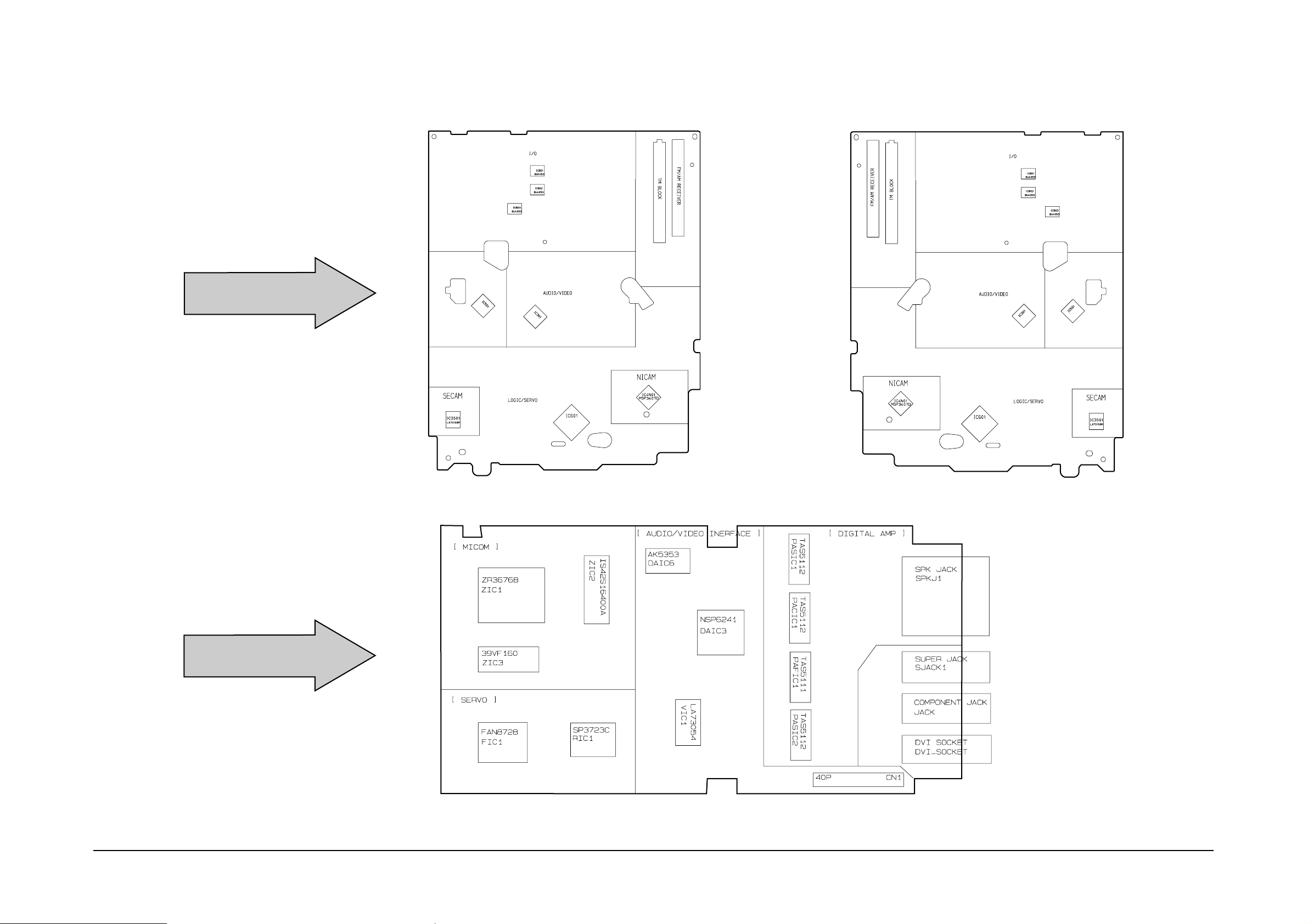
◆ Block Identification of Main PCB
VCR MAIN PCB
<Component Side>
<Conductor Side>
LA72646M
LA71750M
uPD78F4928GF-3BA
LA72646M
LA71750M
uPD78F4928GF-3BA
DVD MAIN PCB
<Component Side>
Page 3
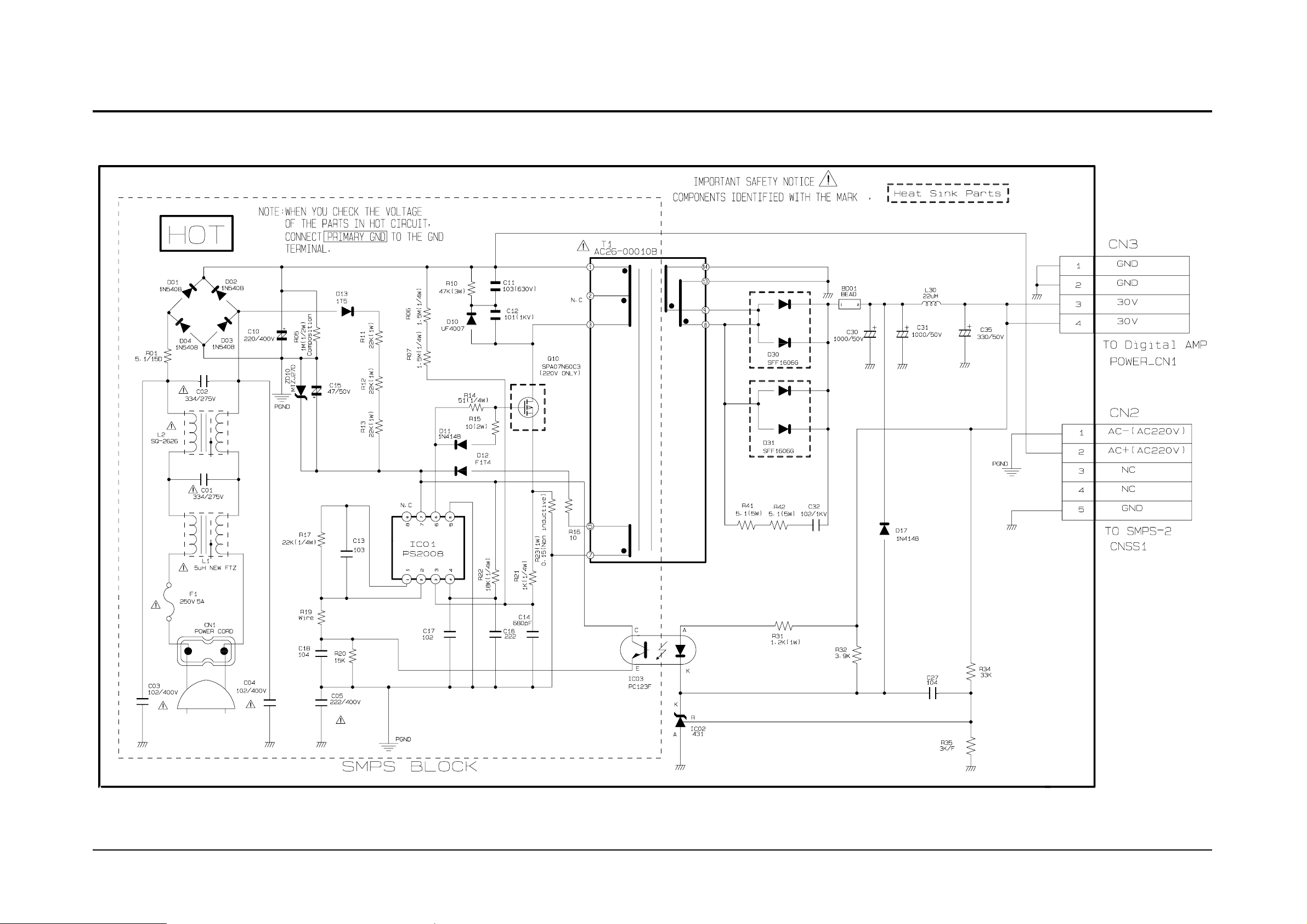
6-1 S.M.P.S.-1
Schematic Diagrams
Samsung Electronics 6-3
This Document can not be used without Samsung’s authorization
Page 4
Schematic Diagrams
6-4 Samsung Electronics
This Document can not be used without Samsung’s authorization
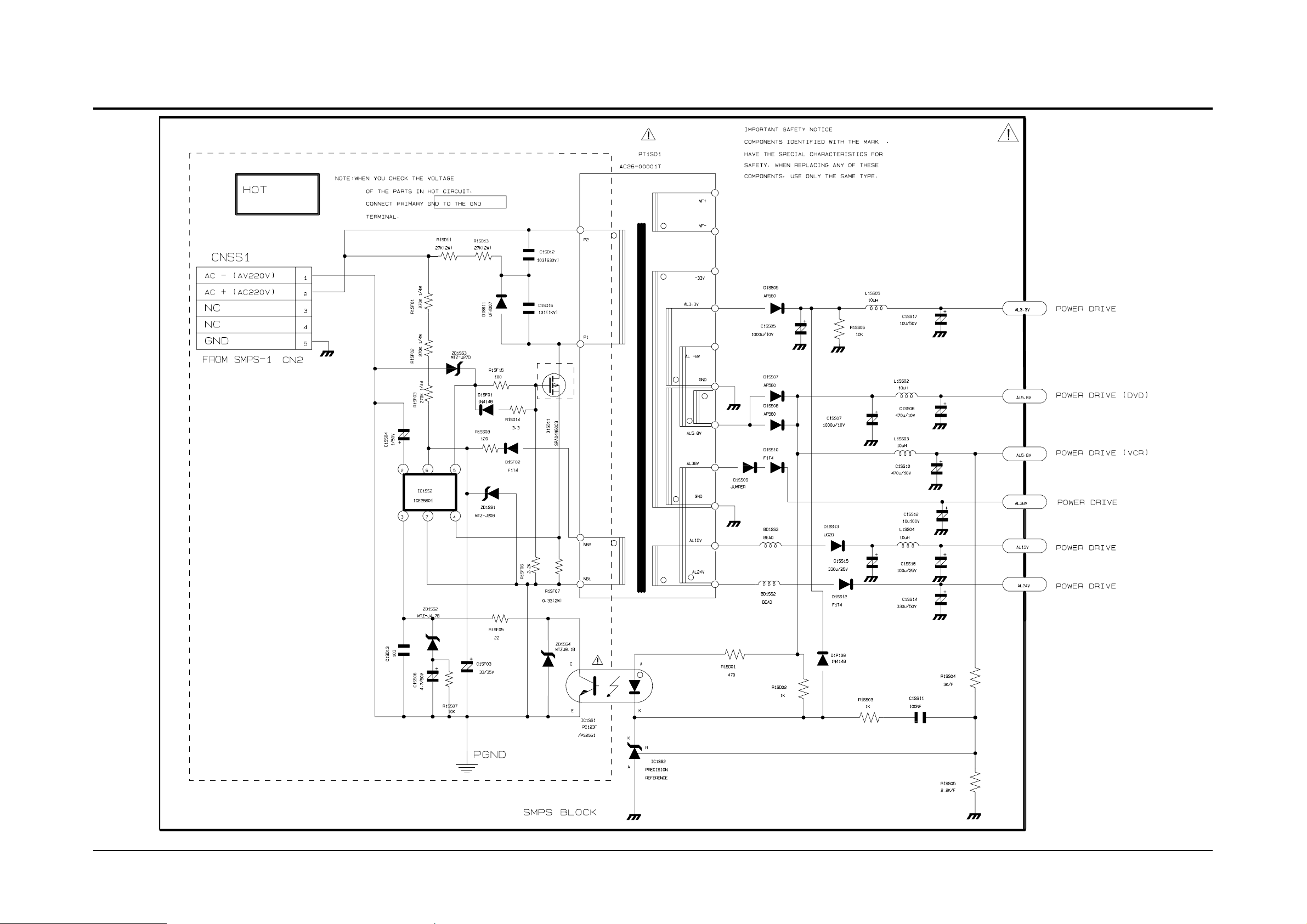
6-2 S.M.P.S.-2
Page 5
Schematic Diagrams
Samsung Electronics 6-5
This Document can not be used without Samsung’s authorization
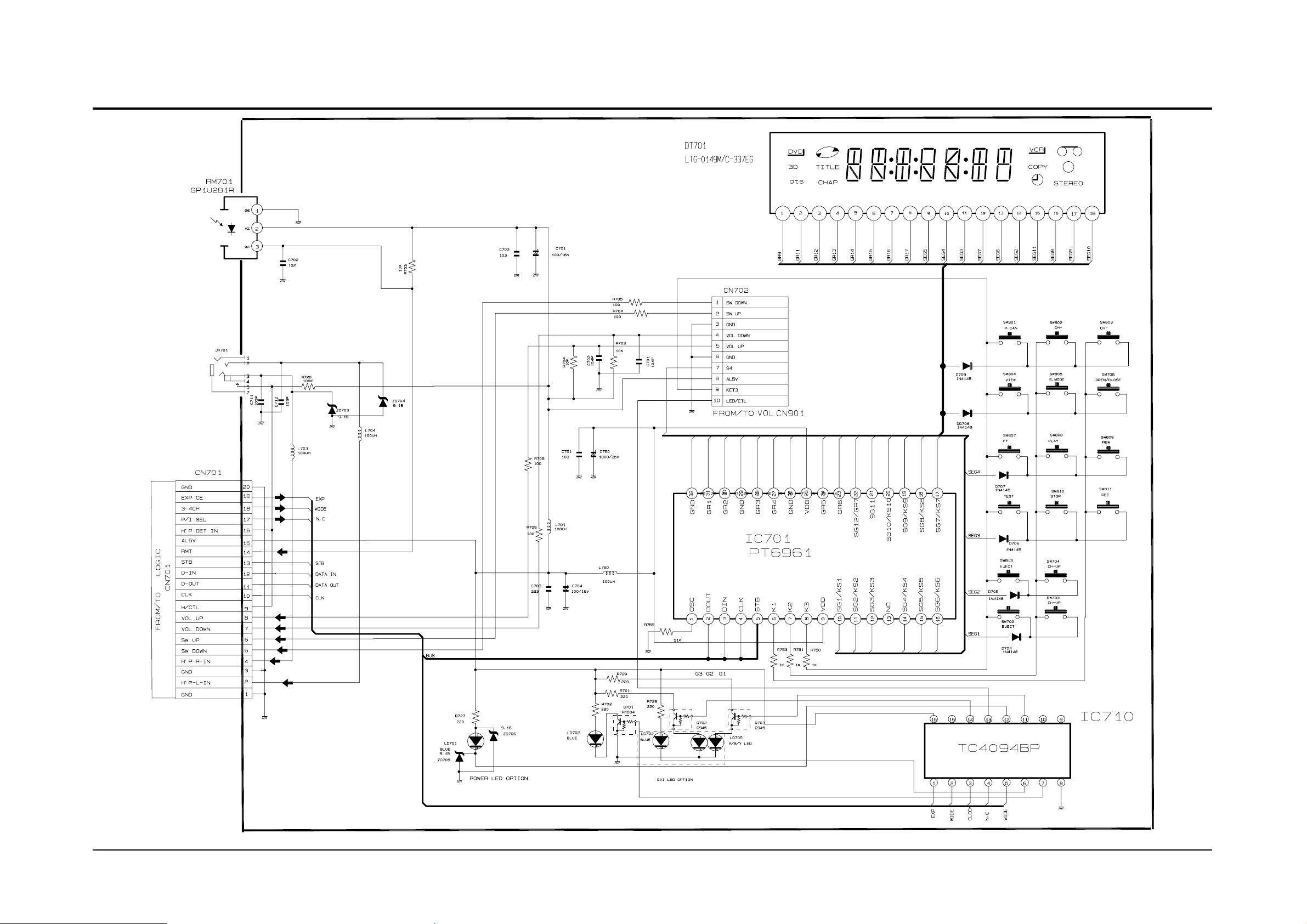
6-3 Function-Timer
Page 6

Schematic Diagrams
6-6 Samsung Electronics
This Document can not be used without Samsung’s authorization
6-4 Volume
Page 7
Schematic Diagrams
Samsung Electronics 6-7
This Document can not be used without Samsung’s authorization
6-5 Power Drive
Page 8
Schematic Diagrams
6-8 Samsung Electronics
This Document can not be used without Samsung’s authorization
6-6 Logic
Page 9

Schematic Diagrams
Samsung Electronics 6-9
This Document can not be used without Samsung’s authorization
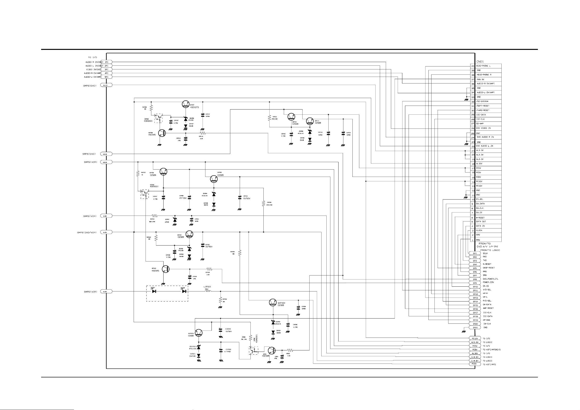
6-7 A/V
Page 10

Schematic Diagrams
6-10 Samsung Electronics
This Document can not be used without Samsung’s authorization
6-8 Hi-Fi
Page 11

6-9 AM/FM Receiver
Schematic Diagrams
Samsung Electronics 6-11
This Document can not be used without Samsung’s authorization
Page 12

Schematic Diagrams
6-12 Samsung Electronics
This Document can not be used without Samsung’s authorization
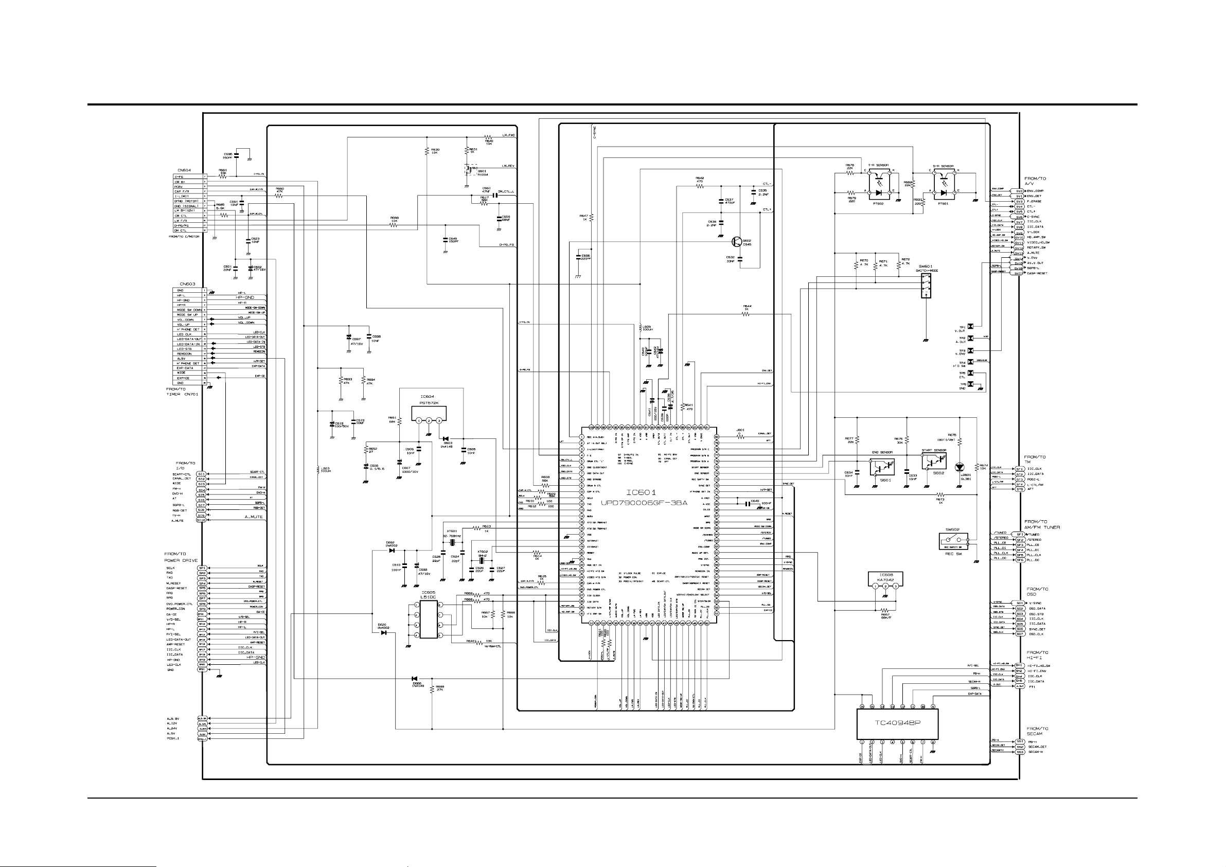
6-10 Input-Output
Page 13
Schematic Diagrams
Samsung Electronics 6-13
This Document can not be used without Samsung’s authorization
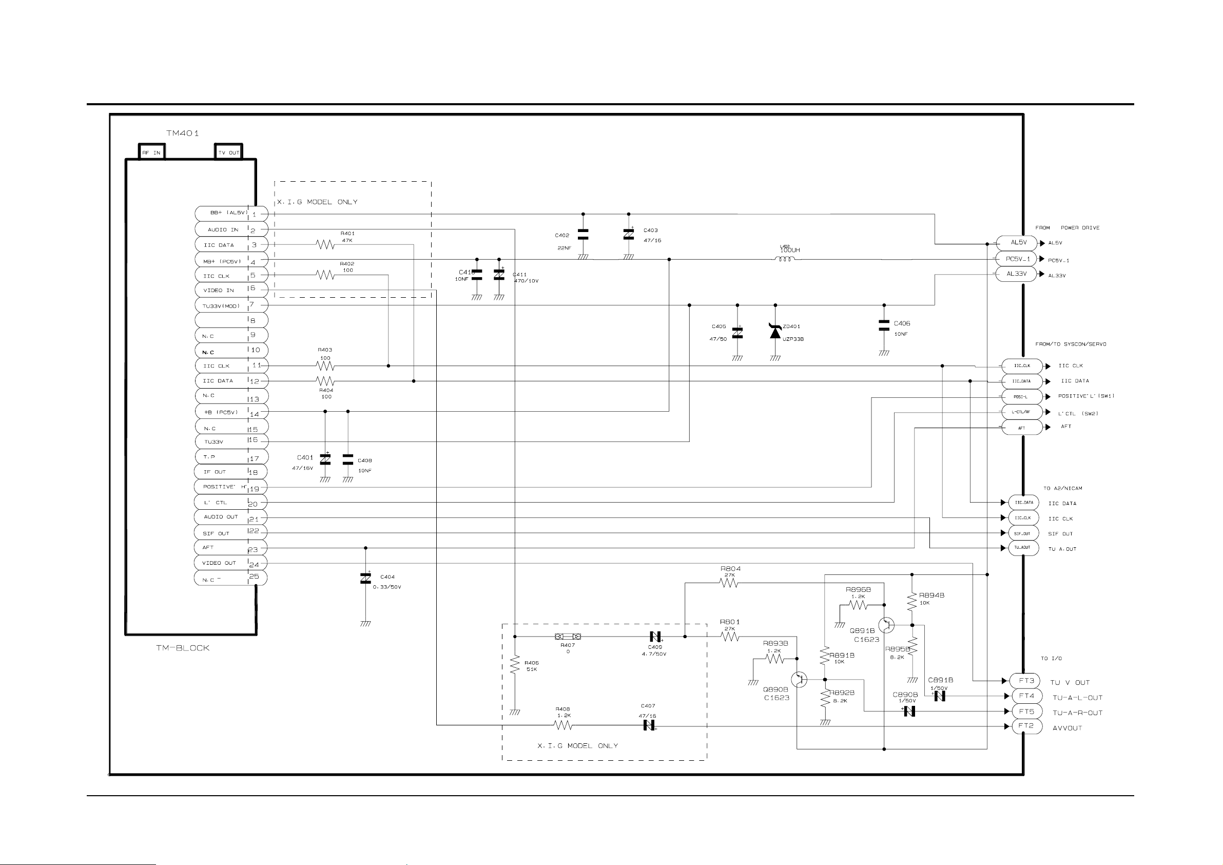
6-11 TM
Page 14

Schematic Diagrams
6-14 Samsung Electronics
This Document can not be used without Samsung’s authorization
6-12 A2/NICAM
Page 15

Schematic Diagrams
Samsung Electronics 6-15
This Document can not be used without Samsung’s authorization
6-13 SECAM
Page 16

Schematic Diagrams
6-16 Samsung Electronics
This Document can not be used without Samsung’s authorization
6-14 OSD/VPS/PDC
Page 17

Schematic Diagrams
Samsung Electronics 6-17
This Document can not be used without Samsung’s authorization
6-15 DVD Micom
Page 18

Schematic Diagrams
6-18 Samsung Electronics
This Document can not be used without Samsung’s authorization
6-16 DVD DVI (CHT-600 Only)
Page 19

Schematic Diagrams
Samsung Electronics 6-19
This Document can not be used without Samsung’s authorization
6-17 DVD Servo
Page 20

Schematic Diagrams
6-20 Samsung Electronics
This Document can not be used without Samsung’s authorization
6-18 DVD Audio/Video Interface
Page 21

Schematic Diagrams
Samsung Electronics 6-21
This Document can not be used without Samsung’s authorization
6-19 Digital Amp
Page 22

Schematic Diagrams
6-22 Samsung Electronics
This Document can not be used without Samsung’s authorization
MEMO
 Loading...