Samsung CGP1607 Troubleshooting

SyncMaster 1000s (CGP1607L) 7-1
7 Troubleshooting
7-1 Parts Level Board Repair Section
Notes: 1. If a picture does not appear, fully rotate the brightness and contrast controls clockwise and reinspect.
2. Check the following circuits.
• No raster appears: Power circuit, Horizontal output circuit, H/V control circuit, and H/V output circuit.
• High voltage develops but no raster appears: Video output circuits.
• High voltage does not develop: Horizontal output circuits.
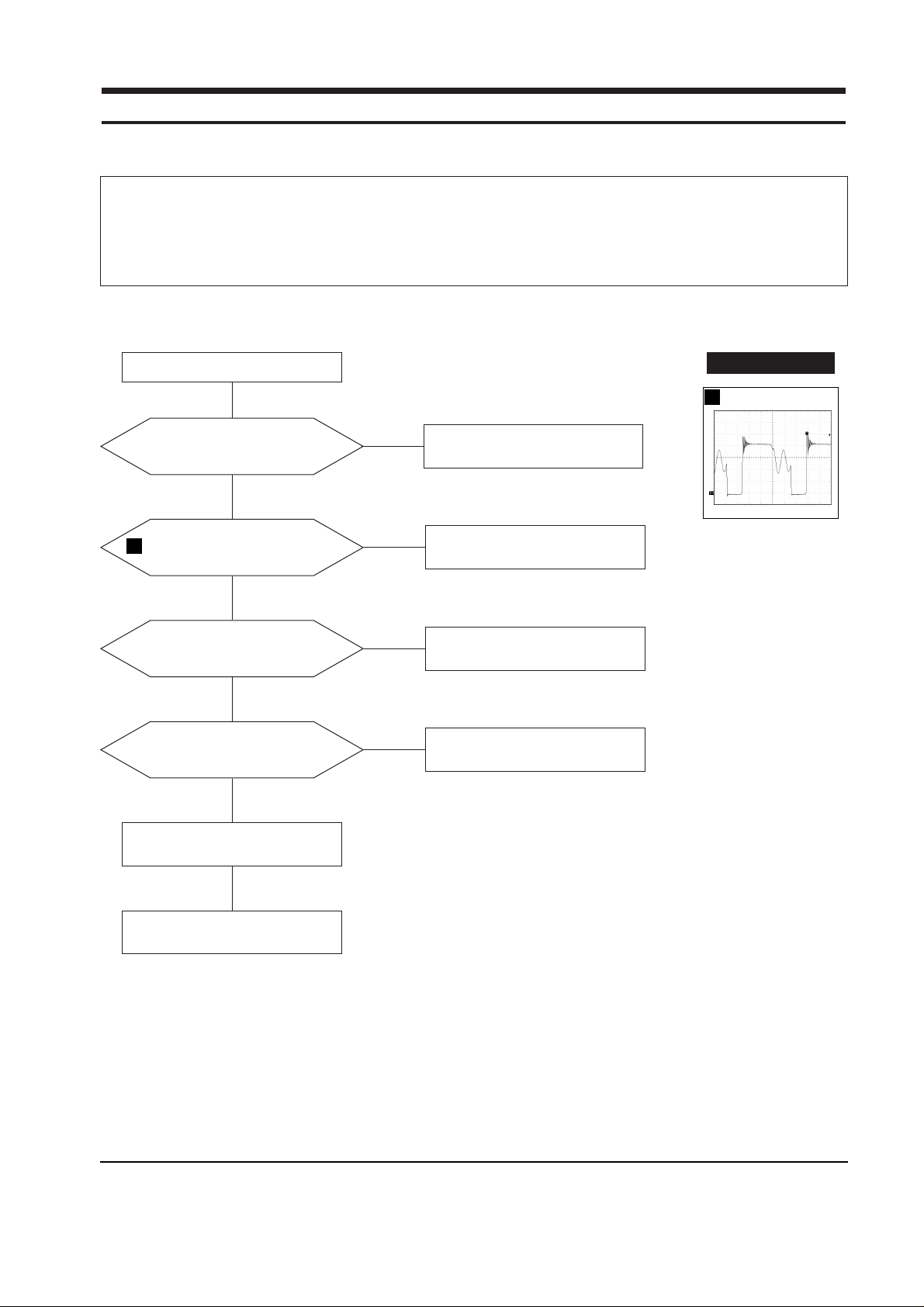
7-1-1 No Power Supply
Does power supply make chirping
noise?
Check and replace Q604, Q607, T601
and D634.
Check and replace FH601, D601.
Verify voltages.
Done.
No
Yes
Does the IC601 Pin 1
waveform correct?
Check and replace IC601, OP602,
IC604 and D606.
Yes
No
Do OP602, IC604 and
D606 work normally?
Relace parts and verify voltages.
Yes
No
Is the power board work well?
Replace power board.
Yes
No
WAVEFORMS
2
552 V (IC601, #1))
CH1 P-P = 552 V CH1 RMS = 323 V
2

7 Troubleshooting
7-2 SyncMaster 1000s (CGP1607L)
7-1-2 DPMS Failure
Make No H/Vsync signal from
signal source. (Power off mode)
Check H/V_sync signal and Video
level of signal source.
Is Amber LED blinking?
Check IC201 Pin 31.
Yes
No
Is the +12 V line off?
Check IC201 Pin 1 and Q417, IC405.
Yes
No
Is the Q608 Base input correct?
Check Pin 2 of IC201 and Q608.
Yes
No
Is the Q602 Base Input correct?
Refer to 7-1-1 No Power Supply.
Done
Yes
No

7 Troubleshooting
SyncMaster 1000s (CGP1607L) 7-3
7-1-3 H_Deflection Failure
Is the IC401 Pin 6
waveform correct?
Is the Q405 source
waveform correct?
Check Q405, R419, R423, D405 and
+195 V line.
Yes
Yes
No
Check R401 (+12 V line), IC401 Pins
5, 6 and 7 and replace IC401.
No
Do the Q406 gate and
drain waveforms
match #18, #28?
Check Q406, D409 and +80 V line.
Yes
No
Do the Q407 base and
collector waveforms
match #29?
Check and replace Q407, D413 and
DY connector connection.
Yes
No
IC403 Pin 4 waveform is right?
Replace IC403.
Check some parts around
Q415 and Q416.
Check some parts around Q413.
Yes
No
Does the IC403 Pin 26
waveform match #44?
Check some parts around IC403.
Yes
No
WAVEFORMS
26
27
18
28
29
43
44
14.16 V (H_DRIVE)
CH1 P-P = 14.16 V CH1 RMS = 8.1 V
18
1.160 kV (Q407, Collector)
CH1 P-P = 1.160 kV CH1 RMS = 300 V
29
13.28 V (IC401, #6)
CH1 P-P = 13.28 V CH1 RMS = 7.5 V
26
216 V (T402, #6)
CH1 P-P = 216 V CH1 RMS = 151 V
27
51.6 V (Q406, Drain)
CH1 P-P = 51.6 V CH1 RMS = 22.6 V
28
3.48 V (IC403, #4)
CH1 P-P = 3.48 V CH1 RMS = 2.898 V
43
12.40 V (IC403, #26)
CH1 P-P = 12.40 V CH1 RMS = 8.188 V
44

7 Troubleshooting
7-4 SyncMaster 1000s (CGP1607L)
7-1-4 S Correction Failure
Are the S1~S5 signals at each
frequency block correct?
Check S1 ~ S5 signal.
Check and replace Q408~Q412, Q414,
C434, C435, C436, C437 and C438.
Yes
7-1-5 H_Lin. Failure
Does the IC201 Pin 4 voltage vary
with different H_Lin. DAC values?
Does the IC402 Pin 4 voltage vary
with different H_Lin. DAC values?
Check +12 V, –14 V line and some
parts around IC402.
Check L406.
Yes
Yes
No
Check and replace IC201.
No
Replace IC201.
No
7-1-6 Invariable H_Size
Does the IC403 Pin 28 voltage vary
with different H_Size DAC values?
Does the IC401 Pin 6 output
duty vary with different H_Size
DAC values?
Check some parts around IC401
and IC403 Pin 28.
Yes
No
Check and replace IC403.
No

7 Troubleshooting
SyncMaster 1000s (CGP1607L) 7-5
7-1-7 Abnormal H_Size
Does the IC201 Pin 5 output
duty vary with different B+ offset
DAC values?
Does the T402 Pin 8
waveform match #14?
Check and replace T402.
Check some parts around D408.
Yes
Yes
No
Check and replace IC201, some
parts IC201 Pin 5,
IC403 Pin 28 and IC401 Pin 2.
No
7-1-8 Side Pin or Trap Failure
Does the IC403 Pin 24 output
match #16?
Yes
Check and replace IC403.
Replace IC403.
Check and replace IC401.
Check some parts IC401 Pin 2
and IC403 Pin 24.
7-1-9 Para. or Pin Balance Failure
Does the IC403 Pin 5 output vary
with different DAC values?
Yes
Done.
No
No
WAVEFORMS
WAVEFORMS
14
16
3.32 V (IC403, #12)
CH1 P-P = 3.32 V CH1 RMS = 0.83 V
14
1.64 V (IC403, #24)
CH1 P-P = 1.64 V CH1 RMS = 3 V
16

7 Troubleshooting
7-6 SyncMaster 1000s (CGP1607L)
7-1-10 Tilt Failure
Does the IC201 Pin 6 output duty
vary with different DAC values?
Does the IC404 Pin 3 output vary
with different DAC values?
Check and replace IC404, +12 V line
and –12 V line.
Check and replace CRT.
Yes
Yes
No
Check and replace IC201.
No
Check tilt connector connection at
CN405.
7-1-11 V Deflection Failure
Is the +14 V, –12 V line DC
output correct?
Does the IC403 Pin 23 output
waveform match #17?
Check and replace IC403.
Yes
Yes
No
Refer to 7-1-1 No Power Supply.
No
Does the IC301 Pin 1 input
waveform match #8?
Check and replace IC301.
Yes
No
Does the IC301 Pin 5 output
waveform match #7?
Check and replace some parts
around IC301.
Yes
No
Check V-DY connector connection
CN301.
WAVEFORMS
17
8
7
54.8 V (IC301, #5)
CH1 P-P = 54.8 V CH1 RMS = 6.4 V
7
2.62 V (V_RAMP)
CH1 P-P = 2.62 V CH1 RMS = 0.45 V
8
4.16 V (IC403, #23)
CH1 P-P = 4.16 V CH1 RMS = 3.5 V
17
 Loading...