

Samsung cea455 series Service Manual

c8
SAMSUNG
r
/'
'-
-:.z.
:::JO;
--t
(
SERVICE MANUAL
EGA COLOR MONITOR
CEA455*
""
I
.......
~
nil
l:I
L-----1
..
.
~
Ir
I
\
"\

CONTENTS
• SPECIFICATION
.........................................................................
2
• IMPORTANT SERVICE SAFETY PRECAUTION
...............................................
3
• THEORY OF OPERATION
................................................................
5
1.
VIDEO
2.
HORIZONTAL & VERTICAL DEFLECTION
3.
POWER SUPPLY
• DISASSEMBLY INSTRUCTION
............................................................
11
• ALIGNMENT INSTRUCTION
..............................................................
12
• TRUOBLESHOOTING GUIDE
.............................................................
16
• WIRING DIAGRAM AND
PARTS
LIST
......................................................
21
• EXPLODED VIEW
.......................................................................
29
• EXPLODED VIEW
PARTS
LIST
...........................................................
31
• ELECTRICAL
PARTS
LIST
................................................................
33
• SCHEMATIC DIAGRAM AND
WAVE
FORM
.................................................
48
• SEMICONDUCTOR LEAD IDENTIFiCATION
.................................................
50
-1-
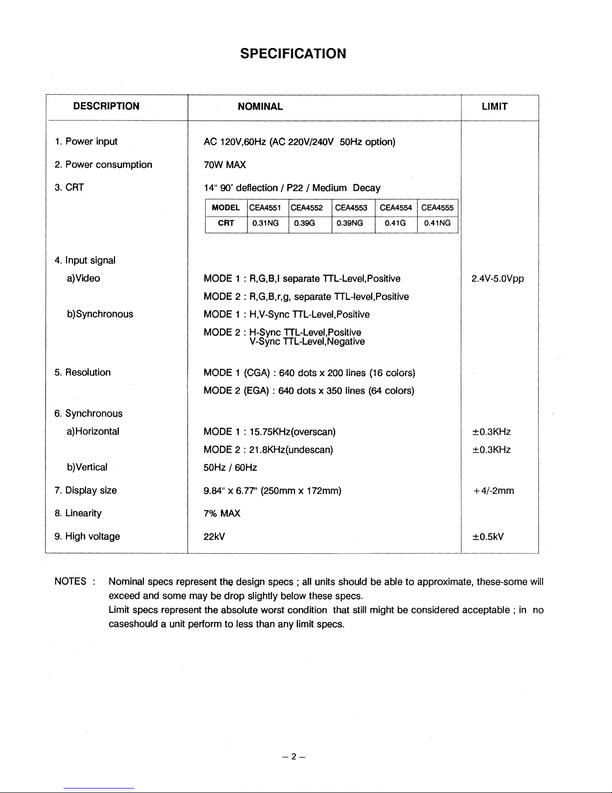
DESCRIPTION
1.
Power input
2.
Power consumption
3.
CRT
4.
Input signal
a)Video
b)
Synchronous
5.
Resolution
6.
Synchronous
a)
Horizontal
b)Vertical
7.
Display size
8.
Linearity
9.
High voltage
SPECIFICATION
NOMINAL
AC 120V,60Hz (AC 220V/240V 50Hz option)
70W MAX
14" 90' deflection / P22 / Medium Decay
MODEL CEA4551 CEA4552 CEA4553 CEA4554 CEA4555
CRT
O.31NG
O.39G
O.39NG
0.41G 0.41NG
MODE 1 : R,G,B,I separate TIL-Level,Positive
MODE 2 : R,G,B,r,g, separate TIL-level,Positive
MODE 1 : H,V-Sync TIL-Level,Positive
MODE
2:
H-Sync TIL-Level,Positive
V-Sync TIL-Level,Negative
MODE 1 (eGA) : 640
dots
x 200 lines (16 COIOiS)
MODE 2 (EGA) : 640
dots
x 350 lines (64 colors)
MODE 1 : 15.75KHz(overscan)
MODE 2 : 21.8KHz(undescan)
50Hz / 60Hz
9.84" x 6.77" (250mm x 172mm)
7%
MAX
22kV
LIMIT
2.4V-5.0Vpp
±O.3KHz
±O.3KHz
+4/-2mm
±O.5kV
NOTES
Nominal specs represent the design
specs;
all units should be able
to
approximate, these-some will
exceed and some may be
drop
slightly below these specs.
Limit specs represent the absolute worst condition that still might be considered
acceptable;
in no
caseshould a unit perform
to
less than any limit specs.
-2-

IMPORTANT SERVICE SAFETY PRECAUTIONS
Service work should
be
perf~rmed
only by qualified
service
technicians who
are
thoroughly familiar with
all
of
the following safety checks
and
servicing guidelines:
WARNING
1.
For continued
safety,
do not attempt to modify
the circuit.
2.
Disconnect the AC power before
serviCing.
3.
Semiconductor
heat
sinks
are
potential shock
hazards when the chassis
is
operating.
SERVICING THE HIGH VOLTAGE SYSTEM
AND
PICTURE TUBE
When
servicing the high voltage
system,
remove
the static charge by connecting a 10kohm
resis-
tor
in
series
with
an
insulated wire (such
as
a
test probe) between the chassis
and
the anode
lead.
(The
AC line cord should
be
disconnected
from the
AC outlet.)
1.
The
picture tube
in
this display monitor employs
integral implosion protection.
2.
Replace
with a tube of the
same
type
and
number for continued
safety.
3.
Do not lift the picture tube by the
neck.
4.
Handle the picture tube only when wearing shatter proof goggles
and
after discharging the high
voltage anode completely.
X-RADIATION AND HIGH VOLTAGE LIMITS
1.
Be
sure
all
service personnel
are
aware of the
procedures
and
instructions covering X-radia-
tion.
The
only potential source of
X-ray
in
a
current solidstate display monitor
is
the
tube.
However,the picture tube does
not
emit
measurable
X-ray
radiation
if
the high voltage
is
as
specified
in
the "high voltage
check"
instruction.
It
is
only when high voltage
is
excessive that
X-radiation
is
capable of penetrating the
shell
of
the picture
tube,
including the
lead
in
glass
material.
The
important precaution
is
to
keep
the high voltage below the maximum
level
specified.
2.
It
is
essential that servicemen
have
available
at
all
times
an
accurate high voltage
meter.
The
calibration of this meter should
be
checked
periodically.
3.
High voltage should always
be
kept
at
the
rated
value-no higher. Operation
at
high voltages
may
cause a failure of the picture tube or high voltage
circuitry and,also under certain conditions,may
produce radiation
in
excess of desirable
levels.
4.
When
the high voltage regulator
is
operating
properly there is no possibility of
an
X-radiation
problem.
'
Everytime a color chassis
is
serviced,the bright-
ness
should
be
tested while monitoring the high
. voltage with a meter to
be
certain that the high
voltage does not exceed the specified
value
and
. that it
is
regulating correctly.
5.
Do not
use
a picture tube other than that
specified
or
make unrecommended circuit
modifications to the high voltage circuitry.
6.
When
trobleshooting or taking test
measure-
ments on a display monitor with excessively high
voltage, avoid being unnecessarily close to the
display monitor.
Do
not operate the display
monitor longer than
is
necessary to locate the
cause of excessive voltage.
-3-
BEFORE RETURNING THE DISPLAY MONITOR
Fire and Shock Hazard
Before returning the display monitor
to
the
user,perform the following safety checks:
1.
Inspect
all
lead
dress to make certain that the
leads
are
not pinched or that the leads
are
not

lodged between the chassis
and
other
metal
parts
in
the display monitor.
2.
Inspect
all
protective devices such as nonmetallic control knobs, insulating materials,
cabinet backs, adjustment and compartment
covers or shields,isolation resistor-capacitor networks, mechanical insulators,etc.
3.
To
be
sure that no shock hazard exists,check
for
leakage current
in
the following manner:
• Plug the
AC
line cord directly into a 120volt
AC
outlet.
(Do
not
use
an
isolation transformer for
this test)
• Using two clips
leads,
connect
1.5
kohm,
10
watt
resistor
paralleled by a 1.5uF capacitor
in
series
with
all
exposed metal cabinet parts
and
a known
earth ground such
as
electrical conduit or
electrical ground connected to earth ground.
•
Use a SSVM
or
YOM
with
1000
ohms per-volt
or higher sensitivity to measure the
AC
voltage
drop across the resistor.
(See
Figure
1.)
• Connect the resistor
to
all
exposed metal parts
having a return path
to
the chassis(metal cabinet,
screw
heads,
knobs
and
shafts,escutcheon,etc.)
and
measure the
AC
voltage drop across the
resistor.
• Any reading of
O.3volt
RMS
(this corresponds to
0.5milliamp.AC) or more
is
excessive and
indicates a potential shock hazard which must
be corrected before returning the display monitor
to the
user.
SAFETY NOTICE
Many electrical
and
mechanical parts which
have
special characteristics
in
this chassis often
pass
unnoticed and the protection afforded by them
can not necessarily
be
obtained by using
replacement components rated for higher voltage,
wattage,
etc.
Replacement parts that
have
these special safety
characteristics are identified
in
this manual,and
its supplement; electrical components having
such features are identified by a !
in
the Parts
List and
Schematic Diagrams.
Before replacing any of these components,read
the Parts List
in
this manual carefully.
The
use
of substitute replacement parts that do not
have
the same safety characteristics
as
specified
in
the Parts List may create shock,
fire,
or other
hazards.
-4-
AC
VOLllETER
1500
n
TO
EXPOSED
METAL
PARTS
TO
KNJWEN
EARTH
GROUND
FIG. 1 LEAKAGE
CURRENT
TEST
CIRCUIT

THEORY OF OPERATION
GENERAL
CEA4551
is
a high resolution color display using a
0.31
dot pitch
NON-GLARE
CRT.
(CEA4552 ; 0.39
glare
CRT,CEA4553 ; 0.39
non-glare
CRT,
CEA4554
;
0.41
glare
CRT , CEA4555 ; 0.41
non-glare
CRT)
It
uses
R,
G,
B,
I or
R,
r,
G,
g,
B, b TTL
input Video
Signals
and
separate
TTL
sync signals.lt
can
operate
in
16
colors
640
by
200
overscan mode or 64colors
640
by
350
underscan mode. This two mode
Is
automatically switched by the polarity of vertical
frequency.
VIDEO
I. Video
Drive Circuit
The
video signals
are
applied to
CUSTOM
IC
(IC1
01).
The
output signals of
IC101
are
applied
to
IC103
which
is
an
open-collector Hex-buffer.
The
output signal
level
of
IC103
(R,r,G,g,B,b)
are
controlled by the
BRIGHTNESS
VR
and
SUB-BRIGHTNESS
VR
(VR110)
and the secon-
dary signals
(r,
g,
b)
are controlled by the
CONTRAST
VA.
The
output signals of
IC103
are
to combine
blanking signals
(H,
V blanking).
Primary signals
(R,
G,
B)
and
secondary signals
(r,
g,
b)
are mixed through
R121
and
D116,R123
and
D117,R125
and
D115
respectively
in
mode
2.Then
the signals
are
applied to the
base
of
pre-amp
transistors(0103,0104,0105).
The
output signals of
IC101
in
MODE 1 and
MODE
2 are selected by the
MODE
signal from
pin no.8 of
IC101
(SL205).
2.
VIDEO
(R,
G,
B)
OUTPUT
The
R,G,B
drive system
is
utilized
in
the video
output circuit of this unit.
In
the case of
RED
signal,the combined color
and blanking signals
are
amplfied sufficiently by
the cascode transistor
(0109, 0110)
The
cut-off levels of the picture tube
are
con-
trolled by the
bias
VRs
(VR103,VR1
04,VR1
05)
between 85Vdc and
145Vdc.
These
DC
voltages are taken from pin no.8 of
FBT
(T
403)
and
pin no.14 of
POWER
TRANS
(T601).
The
color signals
and
blanking signals of 0103,
0104
and
0105
are
supplied
to
the
base
of
0110, 0112, 0114.
The
screen grid,
G2,
is
common
in
the
case
of
RED,GREEN
and
BLUE
CATHODE
respectively.
The
drive control
VRs
(VR101,
VR102)
control
the
base
current of 0110, 0114 for white balance
adjustment.
FIG. 2 SYNC
INTERFACE
CIRCUIT
-5-

VERTICAL
AND
HORIZONTAL DEFLECTION CIR-
CUIT
1.
SYNC
INTERFACE CIRCUIT
In
MODE 1 (CGA
MODE),
the polarity of horizon-
tal
and
vertical sync
are
both positive but
in
MODE
2(EGA
MODE)
the polarity of horizontal
sync
is
positive
and
the vertical sync
is
negative.
If the
HN
sync signal
is
applied
in
MODE
1,
then the output voltage
level
from
pin
nO.8
of
IC102
(EX-OR
gate)
is
OV
and the output voltage
level
from pin
no.
3 of
IC102
is positive.
If the
HN
sync signal
is
applied
in
MODE
2,then
the output voltage
level
from pin
no.
8 of
IC102
is
3.2V
and
the output polarity from pin
nO.3
of
IC102
is
negative.
According to the polarity of vertical sync,
MODE 1 and
MODE 2 are
selected automat-
ically.
Vertical
Deflection Circuit
Vertical
circuit
is
composed of
IC102
(74HCTlS86),
IC301
(LA7830).
IC401
(lA7851),
IC402
(MC14053BCP)
and
its
relative circuits.
The
vertical sync signal from
IC102
which polarity
IS
positive or negative is applied to pin no.19 of
IC401.
Pin
no.19 of
1C401
is
connected to the vertical
oscillation circuit.
The
frequency of oscillator
is
controlled by
the
volt-
age
of pin
18
which
can
varied by the
V-HOLD
VR(VR306).
The
output circuit of
1C301
Is
controlled by
V-SIZE
VR(VR
307)
to vary the vertical
size
of the raster,
that
is
related both
MODE 1 and
MODE
2.
But
V-SIZE
of
MODE 1 Is
only controlled by
CGA
V-SIZE
VR(VR402).
Horizontal OSCillator, AFC and Drive Circuit
The
horizontal sync signal with positive polarity
is
applied to pin 1 of
1C401.The
output from the fly-
back transformer
(T403)
is connectored pin 4 of
1C401
as
part of the automatic frequency circuit
(AFC).
H-CENTER
VR(VR407)
determines the posi-
tion of picture
in
MODE 1 and
MODE
2 but
CGA
H-CENTER
VR(VR403)
controls the position of
CGA
picture only.
The
horizontal oscillation frequency
is,
-6-
obtained from pin
12
of
1C401
and
it
is
fed
to the
next
horizontal drive circuit.
The
pulse-switching
mode of the drive
and
output stage
is a reverse
polarity type
and
that's done when the drive transistor
0401
is
on
and
the output transistor 0402
is
off.
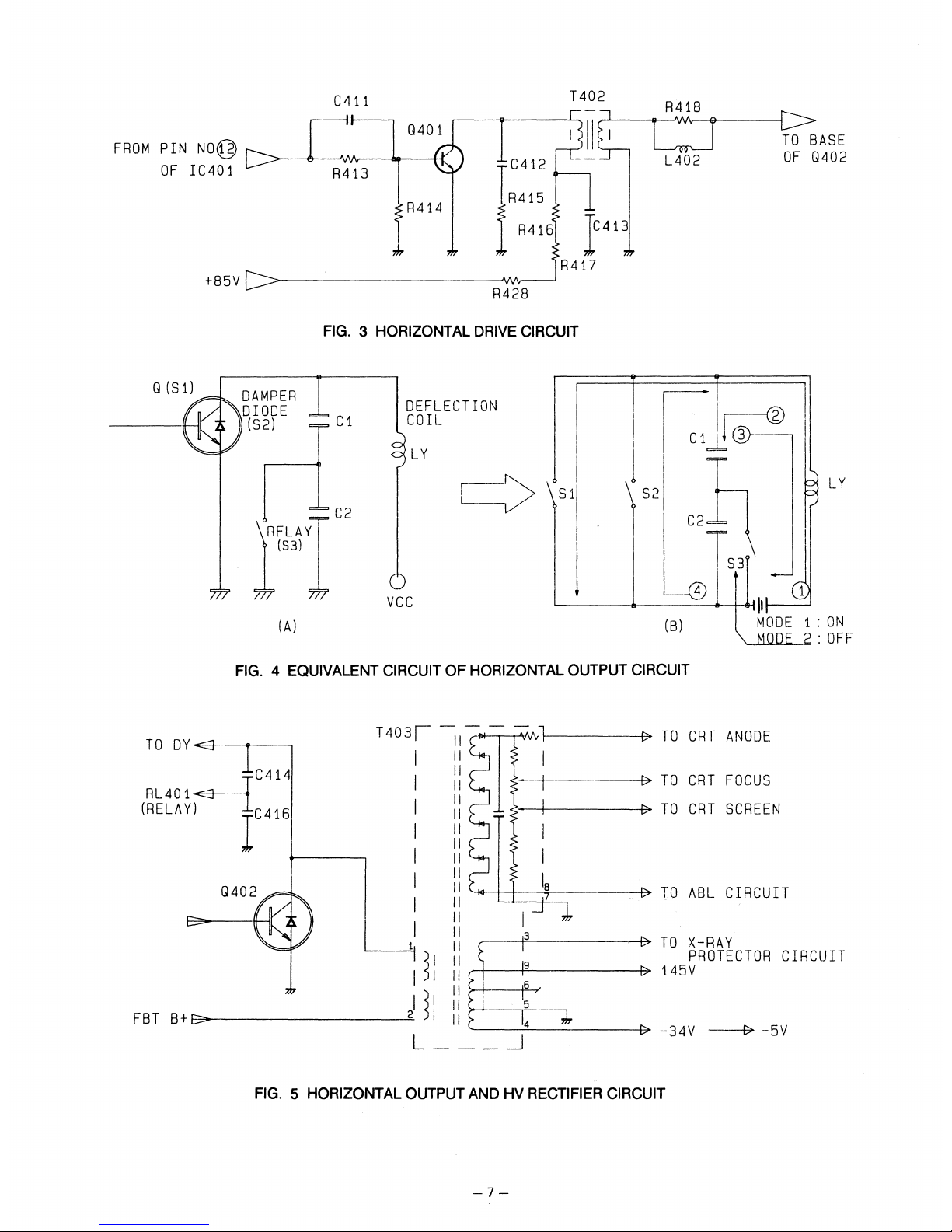
HORIZONTAL
OUTPUT
AND HV RECTIFIER
Horizontal drive voltage which developed at pin
12
of the deflection processor
(IC401)
is
amplified
through the horizontal drive stage (0401)
and
coupled to the
base
of the horizontal output cicuit
via
the horizontal drive transformer(T401).
Refering
to
Fig.3,
the horizontal circuit generates the horizon-
tal scan and high voltage to
be
applied to the picture
tube.
The
function of the horizontal output stage
(0402)
is
to
serve
as
a switch for the horizontal
output circuit.
Refter
to
Fig.4.
During the horizontal scanning period, 0 operates
(S1
is closed,
S2
is opened)
and
the current
is
applied
in
one direction through the horizontal coils
of
the deflection yoke
(ly)
and the capacitor
(MODE
1
:Cl,
MODE
2:C1,C2).
During retrace time, 0 become
to
operate(S1
is
opened,
S2
is
closed)
and
the current
is
applied
In
the opposite direction
through the damper diode
(D),
the horizontal coils of the deflection yoke (ly)
and
the capacitor
Cl,
C2.
The
high voltage required to
be
applied to the anode
of the picture tube
is
generated by boosting the
pulse from the collector of 0402 through
T302
during
the flyback(retrace) period
and
applying this boosted
pulse to a serious of rectifiers.
Refering
to
Fig.5,
high
voltage regulation
is
accomplished internally
in T 403.
HIGH VOLTAGE SHUT-DOWN
SYSTEM
The
shut-down circuit prevents the high voltage from
rising above a presence
level.
Under norminal operat-
ing conditions, this circuit
is
inactive. Operation of
the protector circuit depends upon
an
AFC
pulse,
which apears at pin 3 of the horizontal output
traformer
(T403).
It monitors
an
AFC
pulses sub-
jected to rectification by
D406.
Since it
is
in
propor-
tion to the voltage of that
AFC
pulse,
if the incoming
high voltage increases
and
exceeds its limit, the
AFC
pulse voltage aiso
inceases.
As a result,
there
is
a
larger voltage produced
to
R422
so that its potential
will eventually
be
higher than the voltage( +
8.2V}
of
FROM
PIN
NO@
OF
IC401
+B5V
Q
(S
1)
C411
T402
R418
-II
;::J...-L-
j
----tt--iWv---j.--.--C>
tl
~
TO
BASE
L402
OF
Q402
R428
FIG. 3 HORIZONTAL DRIVE CIRCUIT
o=b
C1
DEFLECTION
COIL
LY
\RELAYI
C2
1.IS31
C=:>
vec
(A)
(B)
MODE
1:
ON
MODE
2:
OFF
FIG. 4 EQUIVALENT CIRCUIT
OF
HORIZONTAL OUTPUT CIRCUIT
TO
DY
~I--~---,
C414
RL401---=-J
(RELAY~C416
I
T403l11
(~lrl~---~f>
TO
CRT
ANODE
I
II~
I
II
Iii:
!
+II-----&[)
TO
CRT
FOCUS
+.
-----&[)
TO
CRT
SCREEN
I
II
I
I
II
,
II
I
I
::
18
~-+-l---'l----~
TO
AB
L C I
RCU
IT
I
II
I
II
II
1
II
L--~
<I
II
I
51
II
(
3
I
19
1
6
/
~
---,;;0
~
-v
TO
X-RAY
PROTECTOR
CIRCUIT
145V
I < I
::
FBT
B+
F::b
__
---------Ei.
2
51
II
5
1
4
*
....
L
___
.-J
L-
-34V
~
-5V
FIG. 5 HORIZONTAL OUTPUT AND
HV
RECTIFIER CIRCUIT
-7-

the Zener diode(ZD401) turning it
ON.
With
0401
turned
ON,
the X-ray protector of
1C401
operates to
stop the horizontal oscillation,shutting down the
resultant high voltage.
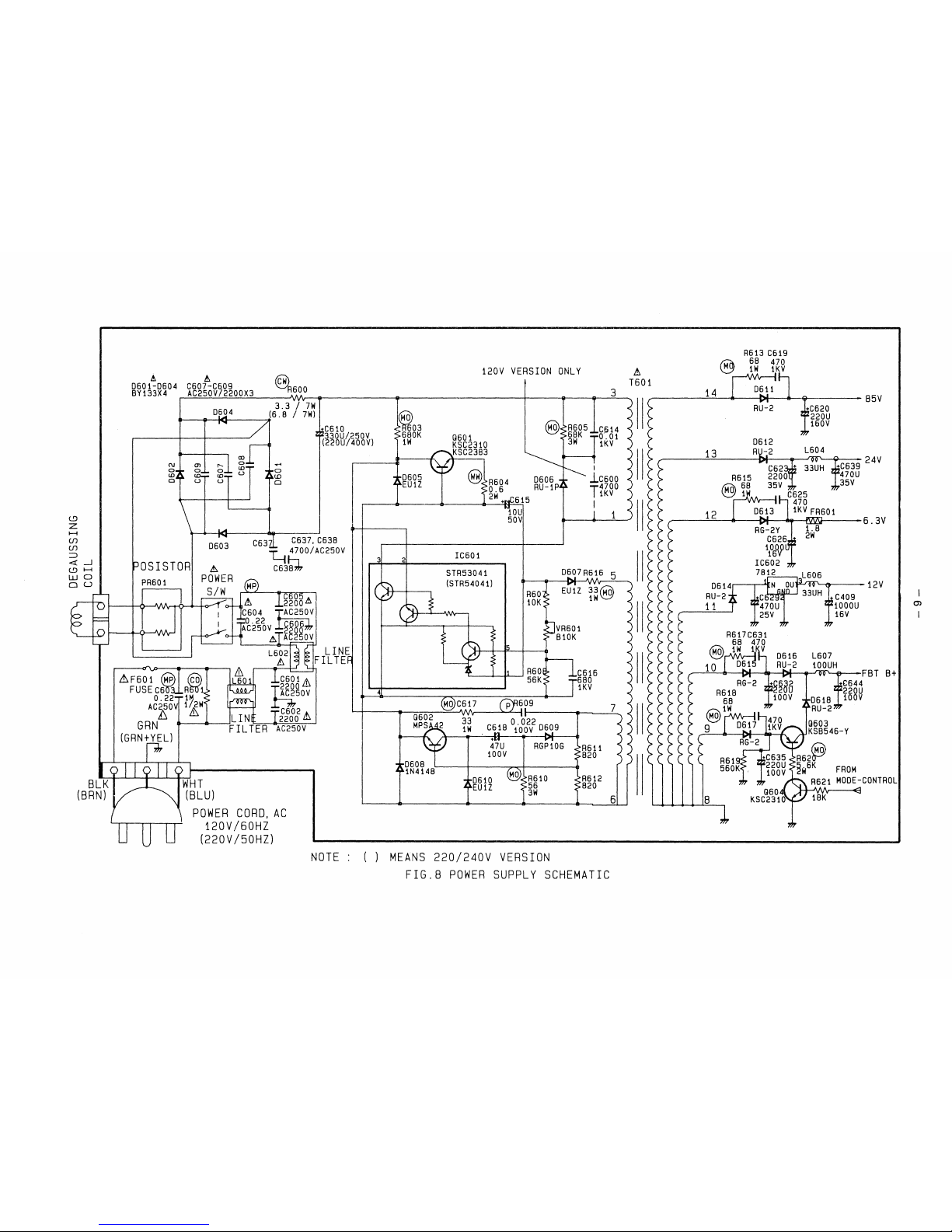
POWER SUPPLY
The
AC
voltage
is
full-wave rectified by the rectified-
smoother circuit and then changed to
DC
voltage
by smoothing capacitor
C610.
When
the power
is
turn
on,
a small current flows into the
base
of output
transistor (included
in
1C601)
via the start-up resistor
(R603).
As
a result, the collector current flows
through the primary windings (pin 1
and
pin 3 of
the power transformer
T601)
and then it produces
an
electromagnetic force.Therefore some voltage
is
induced between pin 6 and pin 7 (driving winding)
of the power tranormer. The induced voltage
is
positively feedback to the base of the output transistor (included
in
1C601)
to increase the
base
current
of this transistor.
As
a result of this base current,
the
collector current of that transistor
is
increased.
The
above operation occurs instaneously to impress
suffiecient base current. The
small signal transis-
tor(0601) protects
1C601
from the surge current
and
0602
is
trigger transistor.
The
FBT
B +
is
selected
by the
MODE
detecting circuit.
In
CGA
MODE,
the
FBT
B + voltage comes from pin
10
of
T60
1 but
in
EGA
MODE
the
FBT
B + comes from pin
11
of
T601
by auto mode sensing circuit. Here the mode sensing
circuit let 0604 and 0603 operate.
FROM
PIN@
OF
T403
(AFC
PULSE)
0406
R423
ZD401
0401
AC
INPUT LINE FILTER
(L60
1.
L602)
IC401
f R422
R438
FIG.6
HIGH
VOLTAGE
SHUT
DOWN
SYSTEM
CIRCUIT
RECTIFIER
IC
(1C60
1)
POWER
TRANS
(T60
11
T601
14
DC
85V
13
DC
24V
l-----DC
6.3V
l-----DC
12V
\----DC
54V
(MODE
1)
9
l----DC
65V
(MODE
2)
FIG. 7 POWER
SUPPLY
BLOCK
DIAGRAM
-8-
(..')
Z
H
U1
U1
::l
<!-.l
(..') H
wo
au
(
\D
~
~
A
t,
0601-0604
C607-C609
BYI33X4 AC250V/2200X3
@
R600
3.3 / 7W
oPJl4
(6.8 / 7W)
.......-
__
........
G---/~
+C610
IF330U//250V
(220U 400V)
!MOl
.¥603
"?680K
IW
A613 C619
r.:;;,.
68
470
6
IW
~K';
14 1
0611
1
II
,..---~2--+--1>
.....
+--+--1(----
85V
AU':2
z~C620
i"220U
@ R605
C.614
IT
160V
G601
~3~KI
~Kel
0612
KSC2383
~
.
V1
24V
120V
VERSION
ONLY
L!.
T601
3
KSC2310
II
13 RU-2
L604
0605
~~
~
0606
~
-LC600 A615
2200
470U
l..'::..rL)
-............-............
I
~
C62:~.
33UH
!1
C639
~~EU1Z
~
A604
4700
(
r.AiiI
68 35V 35V
.-
__
-----t!>-------<l>-g-W-'~t:t=6'_i15
RU
- I P
;>.
T I K V
II
~
6
1
0
~A
-11-,
C
~~5
~IOU
1 1
>-
12
0613
lIKV.!.e,601
50V
Ij-----=-~ ~ ~
r">----=-='---<!>--A-i'G>t:.:.-
2Y
---..--f!
~lofJ1..
8~--
6 . 3 V
...
0603
C6371
C637. C638
J~
4700/AC250V
C63~
POSISTOR
PR601
v J
~
POWER
eo..
S / w
r'~~~P)<---_"","",,,,,--
~Ut,
J:~~88L!;
1---t--Q---'VII'r-t-Q-"""'t--'cY
I
<> <>
I
..1g
60 4 ~ 2 5 0 V
I I
TAh~tv
1.~~8f,1
V<>H
Al.TAC250V
'-----
L
602lliJd
LI
N:~
56K
680
>-
>- >-
FO~~6U
~
2 W
II
~ t ~
lC6
106
2
,
o6..tl7R616
5
>- >- >-
7812
L606
.-----f/"--_-t:>t--:--W'v~Q---"--.,)
>- >-
>-
o6Ij4.--.-...1
....
N
.QU,90
12V
R6qj
EUIZ
~~@
)
>-
(>
? RU-2
~&.fU---l
33UH
C409
10K
)
II
>-
? ? 11 q
Z
470U z
~IOOOU
) >->- >-
~,.----=-=---
25
V 16 V
~
)
>->-?
,
~VR601
>->-? R617C631
810K
<
>- >- >-
>-
68
470
)11
~ >-~ ( @~~
0616
L607
) ~ >-
>-
~
10 1
'b~~'l
R~-2
100UH
<
~
..99~:r-FBT
B+
3 2
le601
STR53041
I:::A
(STR54041)
~cJJ~
~
5
t:,.
l'
FILTEr
r---4~\.P--:::-U"""---:-~--'
&
r----<T.~
FUSE
C603.
R%OI
AC250V
.1.F601
(i.1p)
rcm
,lqjj
I~:6&
,----+-¥-1--,
R60(n1616
L..-:t-----------'
lKV
R618RG-
2
z~~~So I ~~~~d
0.22
1M
i~
AC250V
I/jW
~
~
L!.>
ILIN~
T~~~02Lt.
GRN
FIL
TER
AC250V
(GRNl!Ll
<
11911
)~----.....,
~----~~~~M=~~IC~~~~7.---~C0R~160~9------~---7~
[3p
G602
33
C618
0.022
0609
MPS 2 IW
...
100V-",
47U
RGPIOG
100V
0608
,
IN4148
R611
820
68
100V
0618
100V
IW
~
RU-2
~
~:Jt~h
~~g§46-Y
~
R~,J
'¥'
rMOI
A61
0<
I~C635
R62F
560K'
rI5g~
~~6K
FROM
II
BLKI
~
WHT
(BRN)
V
'\
(BLU)
,0610
~,R610
• EUIZ
56
3W
R612
820
",
,IT
k..
R621
MODE-CONTROL
G60
"L1
"""
u U u
POWER
CORD,
AC
120V/60HZ
(220V 150HZ)
NOTE
6
8 KSC2310
18K
~-=--Jr
( )
MEANS
220/240V
VERSION
FIG.S
POWER
SUPPLY
SCHEMATIC
en
I

~
o
I
V
I
IDEO
NPUT
H
V
-SYNC-
-SYNC-
AC
-INPUT
-~
-
h
-~
l
f-r>
r-c-
VIDEO-INTERFACE
IC-BUFFER
TF1-BUFFER
VIDEO
OUPUT
Q103
Q110-Q109
R~B
III
IC101
IC103
III
Q104
Q112-Q111
III
Q105
Q114-Q113
\U
CONTRAST
~
YBRIGHTNES
Q101
Q102
VIDEO-BOARD
L.....-
V-SIZE
V·-HOLD
SYNC-INTERFACE
.~.
~.
V-SYNC
IC
VERT.OSC.
VERT.OUTPUT
DY
IC102
H-SYNC
V I H
401
HOR.OSC.
IC301
<}-
i
H-JoSI
1 &
~
MODE-CONTROL
MODE-SELECT
S/W
HOR.DRIVE
SPCT
H-WIDTH
CGA
(OV)
IC402
Q401
T401
T402
VR305
fr-
EGA
(3.
5V)
Q302 Q303
H-LIN.
cd
C~A
CkEGA
H-POSI
V-SIZE
H-HOLD
HOR.OUTPUT
Q402
FBT
RELAY-DRIVE
RELAY
T403
r-
Q403 Q404
RL401
IDC
65V
(EGA)
r
I
IDC
54 V (CGA)
f---i>DC
90V
f---i>DC
24V
LINE-FILTER
---i>
RECTIFIER
f-------i:>
POWER-SWITCHING ~ SMPS-TRANS
f---i>DC
12V
L601
L602
0601-0604 IC601
T601
DC
6.3V
MAIN-BOARD
OJ
r
o
(")
"
c
»
C)
:D
»
s:
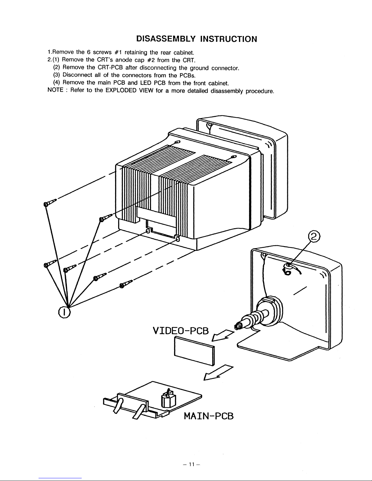
DISASSEMBLY INSTRUCTION
1.Remove the 6 screws #1 retaining
the
rear cabinet.
2.(1)
Remove
the CRT's anode cap
#2
from the
CRT.
(2)
Remove
the
CRT-PCB
after disconnecting the ground connector.
(3)
Disconnect
all
of the connectors from the
PCBs.
(4)
Remove
the main
PCB
and
LED
PCB
from the front cabinet.
NOTE : Refer
to
the
EXPLODED
VIEW
for a more detailed disassembly procedure.
-
11
-
NO
1
2
3
4
5
6
7
8
9
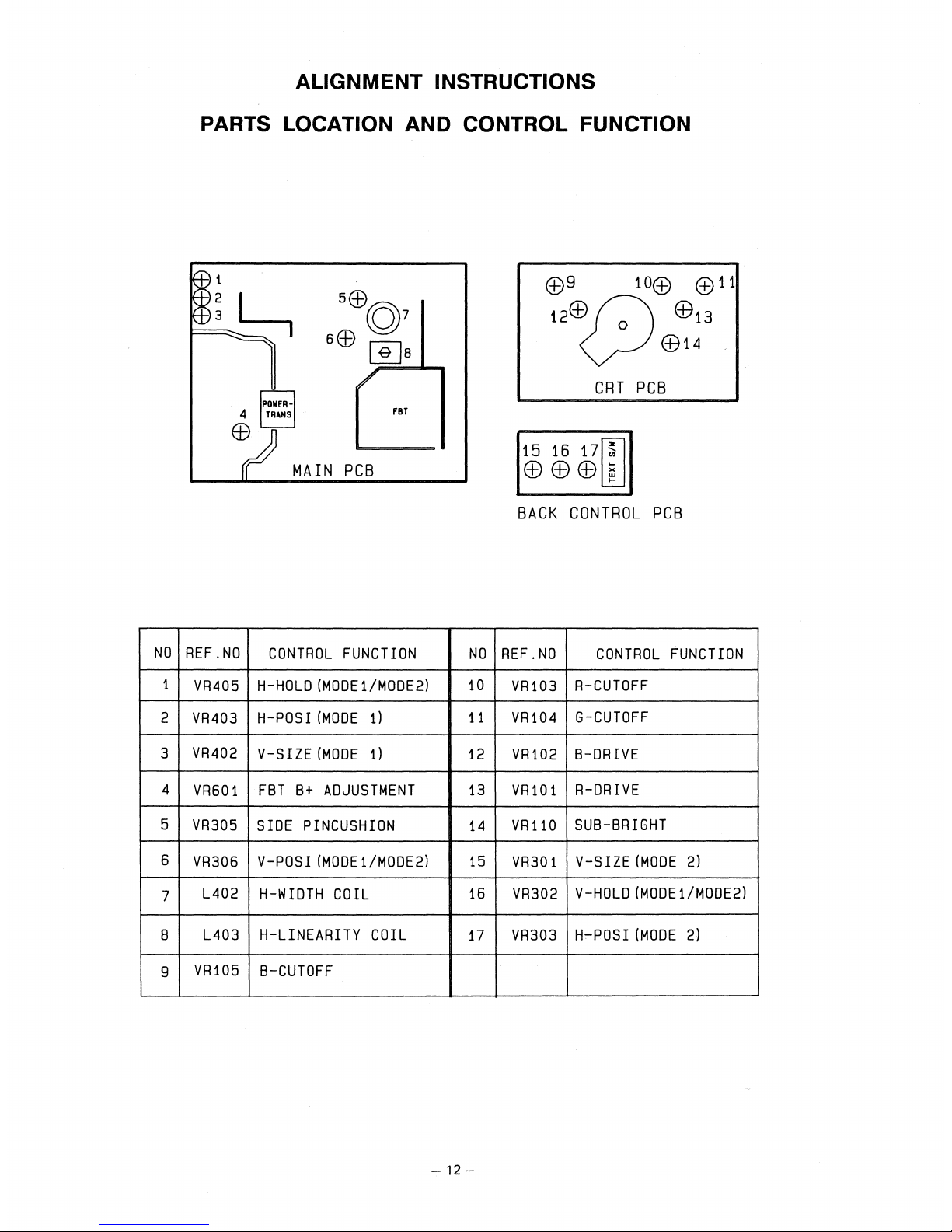
ALIGNMENT INSTRUCTIONS
PARTS LOCATION
AND CONTROL FUNCTION
1
2
3
REF.NO
VR405
VR403
VR402
VR601
VR305
VR306
L402
L403
VR105
FBT
PCB
CONTROL
FUNCTION
H-HOLD(MODE1/MODE2)
H-POSI
(MODE
1)
V-SIZE
(MODE
1)
FBT
B+
ADJUSTMENT
SIDE
PINCUSHION
V-POSI
(MODE1/MODE2)
H-WIDTH
COIL
H-LINEARITY
COIL
B-CUTOFF
NO
10
11
12
13
14
15
16
17
-
12-
CRT
PCB
151617151
EBEBEBE
>-
BACK
CONTROL
PCB
REF.NO
CONTROL
FUNCTION
VR103
R-CUTOFF
VR104
G-CUTOFF
VR102
B-DRIVE
VR101
R-DRIVE
VR
110
SUB-BRIGHT
VR301
V-SIZE
(MODE
2)
VR302
V-HOLD
(MODE1/MODE2)
VR303
H:-POSI
(MODE
2)

ALIGNMENT PROCEDURE ( UNIT FACING
EAST)
Power supply voltage is 120VAC
160Hz
or
220VAC (240VAC)
150Hz
(OPTION)
1.
POWER
SUPPLY
OUTPUT
VOLTAGE
(FBT
B + )
Connect a
DVM
to the anode of
D615
(GT
pin
is
standing)
and
adjust the voltage to
54V
using
VR601.
CONDITION:
1).
NO
SIGNAL
2).CONTRAST,
BRIGHTNESS
is
MINIMUM
(0
BEAM)
2.
MAIN
PCB
ADJUSTMENT
Unless special comment, adjust the
EXT
VR
at
the mechanical center paint.
2-1)
H-RASTER
CENTERING
Turn the
SCREEN
VR
so
that background
raster
can
be
seen
and control the H-CEN-
TER
S/W
(SW401)
so
that the background
raster
is
on
the center of
CRT.
This must
be
done
in
EGA
MODE
(MODE
2 I
21.8KHz).
2-2)
H-HOLD
ADJUSTMENT
(a)
Disconnect the signal cable
(b)
Connect the frequency counter
at
the
H-DY
WIRE
(RED
wire) and adjust the frequency
in
range of 15.700KHz +
I-50Hz
using
CGNEGA
H-HOLD
VR
(VR405).
* Frequency of
EGA
(MODE
2/21.8KHz)
is
ad-
justed automatically.
2-3)
V-HOLD
ADJUSTMENT
(a)
Disconnect the signal cable.
(b)
Connect the frequency counter at R304(side
of
IC301)
and adjust the frequency
in
the
range of 56Hz
+
1-1
Hz using V-HOLD
VR(VR306).
* If the vertical frequency from
PC
is
50Hz,adjust
the vertical frequency at 46Hz
+
1-1
Hz.
2-4)
H-LINEARITY
ADJUSTMENT
(a)
Connect the signal cable.
(b)
Adjust
L403
to the optimum linearity
in
MODE
1 and
MODE
2 linearity pattern.
-13-
2-5)
H-POSITION
(a)
Adjust
H-CENTER
VR
(VR407)
to the center
of the picture when the signal of
MODE
2
is
applied.
(b)
Change mode
to
CGA MODE (MODE
1/15.75KHz) and adjust H-CENTER
VR
using
CGA
H-POSI
VR(VR403}.
2-6)
SIDE
PINCUSHION
Adjust the side pincushion to the optimum
side pincushion using
VR305.
2-7)
H-WIDTH
a)
Adjust the
H-WIDTH
using width coil
(L402)
so
that
H-WIDTH
is
adjusted
in
the range
250
+ 4/-2MM
in
MODE
2 .
b)
Check the
H-WIDTH
of
MODE
1.
*
H-WIDTH
of
MODE 1 is
adjusted
in
the range
250
+ I-4MM automatically.
2-8)
V-POSITION
Adjust the center of vertical using
v-pas
I
VR(VR306).
*
The
V-POSI
VR
(VR306)
can control vertical
center of
MODE
1,MODE 2 together.
2-9)
V-SIZE
a)
Adjust
V-SIZE
using
V-SIZE
VR
(VR
307)
so
that vertical size
is
172MM
in
MODE
2.
b)
Change to
MODE
2 and adjust vertical
size
to
172MM,
equal
to
MODE
2 vertical
size,
using
CGA
V-SIZE(VR402).
2-10)
FOCUS
ADJUSTMENT
Adjust the focus control to the optimum
position.
2-11)
BLACK
AND
WHITE
TRACKING
a)
Turn the screen control fully clockwise. Turn
the red,green and blue bias controls
mechanical centers.
Set
the brightness con-
trol
and
the
red
and blue drive controls at
the center positions.
b)
Turn the
SW301
to the left.
c)
Rotate the screen control counterclockwise
until a raster (either the
red,
green or blue)
appears dimply on the screen.
Notes:
Adjust
VR104
and
VR105
if
red
is
appears.
Adjust
VR103
and
VR105
if green
is
appears.
Adjust
VR103
and
VR104
if blue
is
appears.
d)
Return the
SW301
to its original position.
e)
Operate the computer
in
such a way that
the entire screen
is
R,
G,
B white.
f)
Rotate the
RED
and
BLUE
drive controls
until the raster
is
white.
g)
Set
the brightness control at its maximum
position and adjust the sub-brightness con-
trol until a reading of
20
+ /-2F/L appears.
h)
Turn the brightness control
in
either direc-
tion to check that the picture maintains a
good white balance.
i)
Repeat
steps
(a)
thru
(h)
for readjustment.
Horizontal:12 Lines
Min.
Vertical:16 Lines
Min.
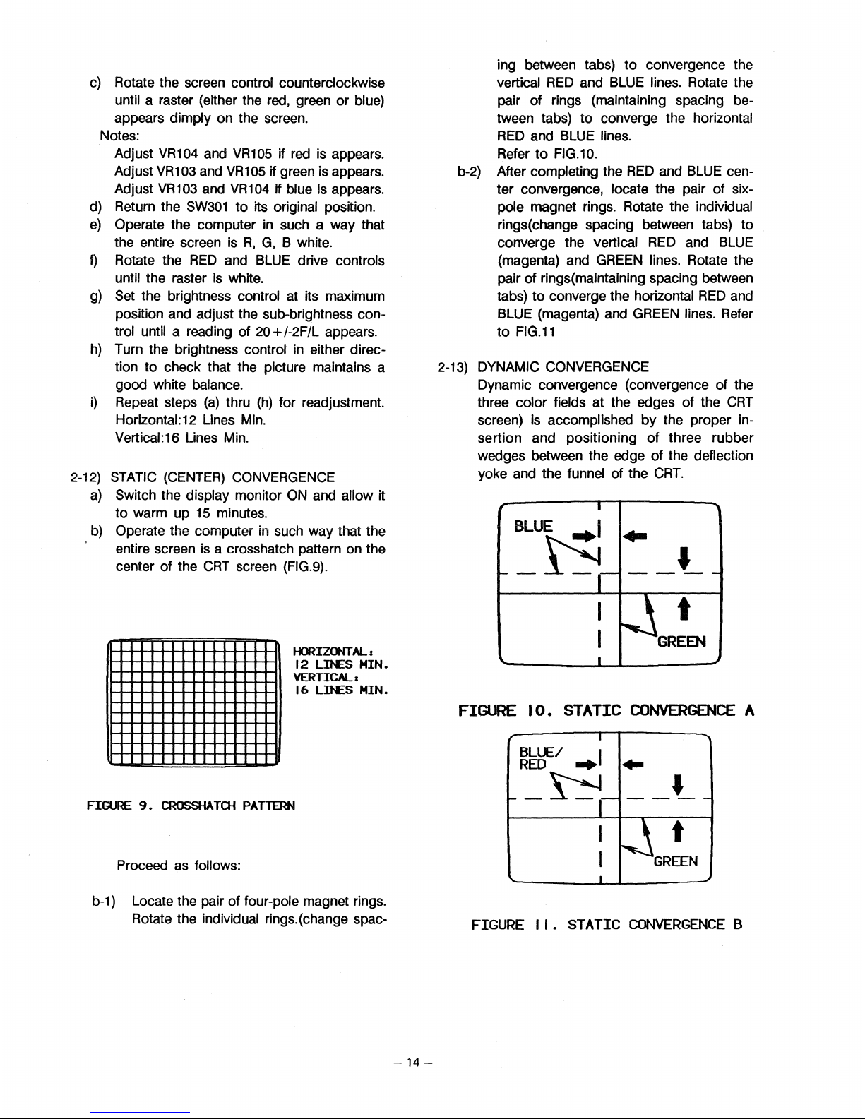
2-12)
STATIC
(CENTER)
CONVERGENCE
a)
Switch the display monitor
ON
and allow it
to warm up
15
minutes.
b)
Operate the computer
in
such way that the
entire screen
is
a crosshatch pattern
on
the
center of the
CRT
screen
(FIG.9).
KlRIZONTAL.
12
LINES
MIN.
VERTICAL
I
16
LINES
MIN.
FIGURE
9.
CROSSHA
Ta-t
PATTERN
Proceed
as
follows:
b-1)
Locate the pair of four-pole magnet rings.
Rotate the individual rings.(change spac-
-
14-
ing between tabs) to convergence the
vertical
RED
and
BLUE
lines. Rotate the
pair of rings (maintaining spacing be-
tween tabs) to converge the horizontal
RED
and
BLUE
lines.
Refer to
FIG.l0.
b-2)
After completing the
RED
and
BLUE
cen-
ter convergence, locate the pair of
sixpole magnet rings. Rotate the individual
rings(change spacing between tabs) to
converge the vertical
RED
and
BLUE
(magenta) and
GREEN
lines. Rotate the
pair of rings(maintaining spacing between
tabs) to converge the horizontal
RED
and
BLUE
(magenta)
and
GREEN
lines.
Refer
to
FIG.11
2-13)
DYNAMIC
CONVERGENCE
Dynamic convergence (convergence of the
three color fields at the edges of the
CRT
screen)
is
accomplished by the proper insertion and positioning of three rubber
wedges between the edge of the deflection
yoke
and
the funnel of the
CRT.
FIGURE
10.
STATIC
CONVERGENCE
A
BLlE/
I
RED
..
....
•
---
-~
t
GREEN
FIGURE
I
I.
STATIC
CONVERGENCE
B
 Loading...