

Samsung CCBP730Q User Manual
V
User manual of CCBP730Q
1. Introduction
CCBP730Q is a Wi-Fi / Bluetooth Combo module compliant with IEEE802.11 a.b.g.n.ac
MAC/baseband/radio applications. The core chipset is from Qualcomm, part number QCA9379-7.
2. Hardware Architecture:
2.1 Main Chipset Information
Item Vendor Part Number
IEEE802.11 a.b.g.n.ac
mac/baseband/radio
Bluetooth 4.2 + HS
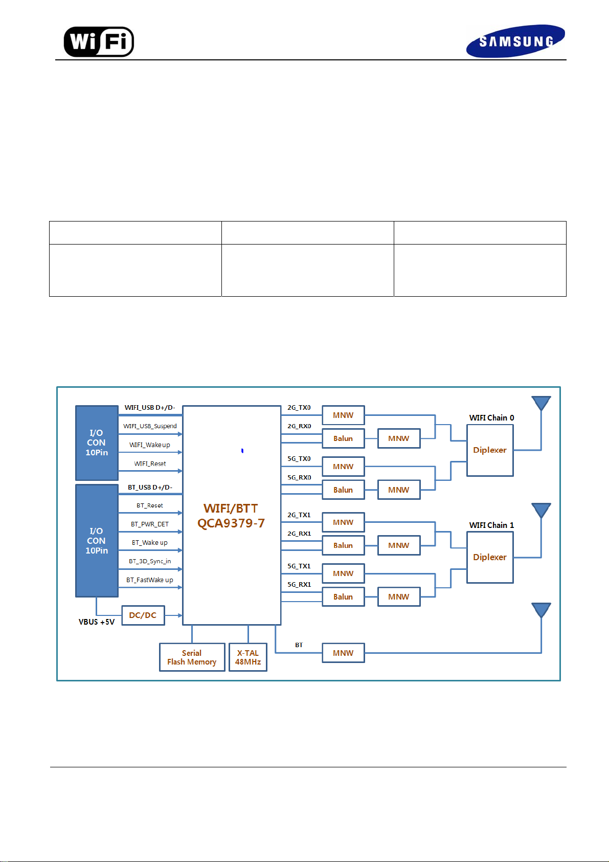
2.2 Circuit Block Diagram
The major internal and external block diagram of
Qualcomm QCA9379-7
CCBP730Q is illustrated in Figure 1-1.
Figure 1-1
CCBP730Q block diagram and System Interface
ersion 1.0 Samsung Electronics page 1 of 6

V
3. Operational Description
CCBP730Q is the 802.11a/b/g/n /ac WIFI Module that acts as a communication controller for users of a
wireless device to connect to Air-Conditioner.
- Features
>IEEE 802.11ac Draft compliant.
>Dual-band 2.4GHz /5 GHz
>Dual-stream spatial multiplexing up to 867Mbps data rate
>Support 20,40,80MHz channel with optional SGI(256QAM modulation)
>On-chip power amplifiers and low –noise amplifiers for both bands
- Time base of the RF frequency
For IF and RF frequency, a crystal(48MHz) is a clock reference.
- Synthesizer
Synthesizer inside Transceiver. Internal voltage controlled oscillator (VCO) provides the desired LO
signal base on the phase-locked loop (PLL) with a relatively wide tuning range for this application.
Internal fractional nPLL allows support for a wide range of reference clock frequencies
- WIFI Transmission
Baseband data is modulated and upconverted to the 2.4GHz ISM and 5-GHz U-NII bands, respectively.
Linear on chip power amplifier are included, which are capable of delivering high output powers while
Meeting IEEE802.11ac and IEEE802.a/b/g/n specifications without the need for external Pas.
When using the internal Pas, closed-loop output power control is completely integrated.
Base-band Processing (BBP) IC has DSSS (BPSK/QPSK/CCK) and OFDM
(BPSK/QPSK/16QAM/64QAM/25QAM) modulation function, it provides transmission data rate are 1, 2,
5.5, 11Mbps on DSSS and 6, 12, 18, 24, 36, 48, 54 Mbps on OFDM. Digital data signal will be converted
to analog (TX IQ) signals through DAC in BBP IC, TX IQ pass through to low pass filter. TX I/Q signal
use direct conversion (zero-IF) architecture converter to generate carrier frequency signal. Transceiver
IC and internal PA magnify output power.
- WIFI Receiver
The QCA9379-7 has a wide dynamic range, direct conversion receiver that employs high-order on-chip
channel filtering to ensure reliable operation in the noisy 2.4GHz ISM band or the entire 5GHz U-NII band
.Control signals are available that can support the use of optional LNAs for each band,which can increase
the receive sensitivity by several decibels.
Reverse direction isolation of LNA inside Transceiver IC suppresses unwanted radiation. Then RF
signal will be directly down to IF signal (RX IQ) and high frequency spurious emissions are suppressed by
LPF. At last RX IQ signal will be demodulated digital data.
ersion 1.0 Samsung Electronics page 2 of 6
 Loading...