

Samsung S3C8248, C8245, P8245, C8249, C8247 User Manual
...
23-S3-C8248/C8245/P8245/C8247/C8249/P8249-032002
USER'S MANUAL
S3C8248/C8245/P8245
/C8247/C8249/P8249
8-Bit CMOS
Microcontrollers
Revision 3

S3C8248/C8245/P8245/C8247/C8249/P8249 PRODUCT OVERVIEW
1-1
1 PRODUCT OVERVIEW
S3C8-SERIES MICROCONTROLLERS
Samsung's S3C8 series of 8-bit single-chip CMOS microcontrollers offers a fast and efficient CPU, a wide range
of integrated peripherals, and various mask-programmable ROM sizes. Among the major CPU features are:
— Efficient register-oriented architecture
— Selectable CPU clock sources
— Idle and Stop power-down mode release by interrupt
— Built-in basic timer with watchdog function
A sophisticated interrupt structure recognizes up to eight interrupt levels. Each level can have one or more
interrupt sources and vectors. Fast interrupt processing (within a minimum of four CPU clocks) can be assigned
to specific interrupt levels.
S3C8248/C8245/P8245/C8247/C8249/P8249 MICROCONTROLLER
The S3C8248/C8245/P8245/C8247/C8249/P8249
single-chip CMOS microcontroller are fabricated
using the highly advanced CMOS process, based on
Samsung’s newest CPU architecture.
The S3C8248, S3C8245, S3C8247, S3C8249 are a
microcontroller with a 8K-byte, 16K-byte, 24K-byte.
32K-byte mask-programmable ROM embedded
respectively.
The S3P8245 is a microcontroller with a 16K-byte
one-time-programmable ROM embedded.
The S3P8249 is a microcontroller with a 32K-byte
one-time-programmable ROM embedded.
Using a proven modular design approach, Samsung
engineers have successfully developed the
S3C8248/C8245/P8245/C8247/C8249/P8249 by
integrating the following peripheral modules with the
powerful SAM8 core:
— Six programmable I/O ports, including five 8-bit
ports and one 5-bit port, for a total of 45 pins.
— Eight bit-programmable pins for external
interrupts.
— One 8-bit basic timer for oscillation stabilization
and watchdog functions (system reset).
— Two 8-bit timer/counter and two 16-bit
timer/counter with selectable operating modes.
— Watch timer for real time.
— 8-input A/D converter
— Serial I/O interface
The S3C8248/C8245/P8245/C8247/C8249/P8249
is versatile microcontroller for camera, LCD and
ADC application, etc. They are currently available in
80-pin TQFP and 80-pin QFP package
OTP
The S3P8245/P8249 are OTP (One Time Programmable) version of the S3C8245/C8249 microcontroller. The
S3P8245 microcontroller has an on-chip 16K-byte one-time-programmable EPROM instead of a masked ROM.
The S3P8249 microcontroller has an on-chip 32K-byte one-time-programmable EPROM instead of a masked
ROM. The S3P8245 is comparable to the S3P8245, both in function and in pin configuration.
The S3P8249 is comparable to the S3P8249, both in function and in pin configuration.

PRODUCT OVERVIEW S3C8248/C8245/P8245/C8247/C8249/P8249
1-2
FEATURES
Memory
• ROM: 32K-byte (S3C8249/P8249)
• ROM: 16K-byte (S3C8245/P8245)
• RAM: 1056-Byte (S3C8249/P8249, S3C8247)
• RAM: 544-Byte (S3C8245/P8245, S3C8248)
• Data memory mapped I/O
Oscillation Sources
• Crystal, ceramic, RC (main)
• Crystal for subsystem clock
• Main system clock frequency 1-10 MHz
(3 MHz at 1.8 V, 10 MHz at 2.7 V)
• Subsystem clock frequency: 32.768 kHz
• CPU clock divider (1/1, 1/2, 1/8, 1/16)
Two Power-Down Modes
• Idle (only CPU clock stops)
• Stop (System clock stops)
Interrupts
• 6 level 8 vector 8 internal interrupt
• 2 level 8 vector 8 external interrupt
45 I/O Pins
• 45 configurable I/O pins
Basic Timer
• Overflow signal makes a system reset.
• Watchdog function
8-Bit Timer/Counter A
• Programmable 8-bit timer
• Interval, capture, PWM mode
• Match/capture, overflow interrupt
8-Bit Timer/Counter B
• Programmable 8-bit timer
• Carrier frequency generator
16-Bit Timer/Counter 0
• Programmable 16-bit timer
• Match interrupt generates
16-Bit Timer/Counter 1
• Programmable 16-bit timer
• Interval, capture, PWM mode
• Match/capture, overflow interrupt
Watch Timer
• Real-time and interval time measurement
• Clock generation for LCD
• Four frequency outputs for buzzer sound
LCD Controller/Driver
• Maximum 16-digit LCD direct drive capability
• Display modes: static, 1/2 duty (1/2 bias)
• 1/3 duty (1/2 or 1/3 bias), 1/4 duty (1/3 bias)
A/D Converter
• Eight analog input channels
• 50 µs conversion speed at 1 MHz f
ADC
clock
• 10-bit conversion resolution
8-Bit Serial I/O Interface
• 8-bit transmit/receive mode
• 8-bit receive mode
• LSB-first/MSB-first transmission selectable
• Internal/external clock source
Voltage Booster
• LCD display voltage supply
• S/W control en/disable
• 3.0 V drive
Voltage Detector
• Programmable detection voltage
(2.2 V, 2.4 V, 3.0 V, 4.0 V)
• En/Disable S/W selectable
Instruction Execution Times
• 400 ns at 10 MHz (main)
• 122 us at 32.768 kHz (subsystem)
Operating Temperature Range
• -40 °C to 85 °C
Operating Voltage Range
• 1.8 V to 5.5 V
Package Type
• 80-pin QFP
• 80-pin TQFP
S3C8249’s ROM version device
• S3C8247 (ROM 24K-byte)
S3C8245’s ROM version device
• S3C8248 (ROM 8K-byte)
S3C8248/C8245/P8245/C8247/C8249/P8249 PRODUCT OVERVIEW
1-3
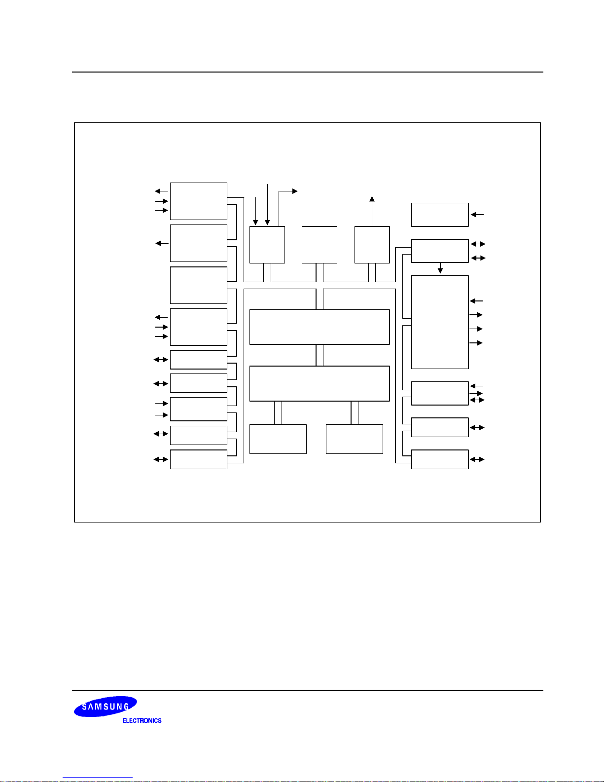
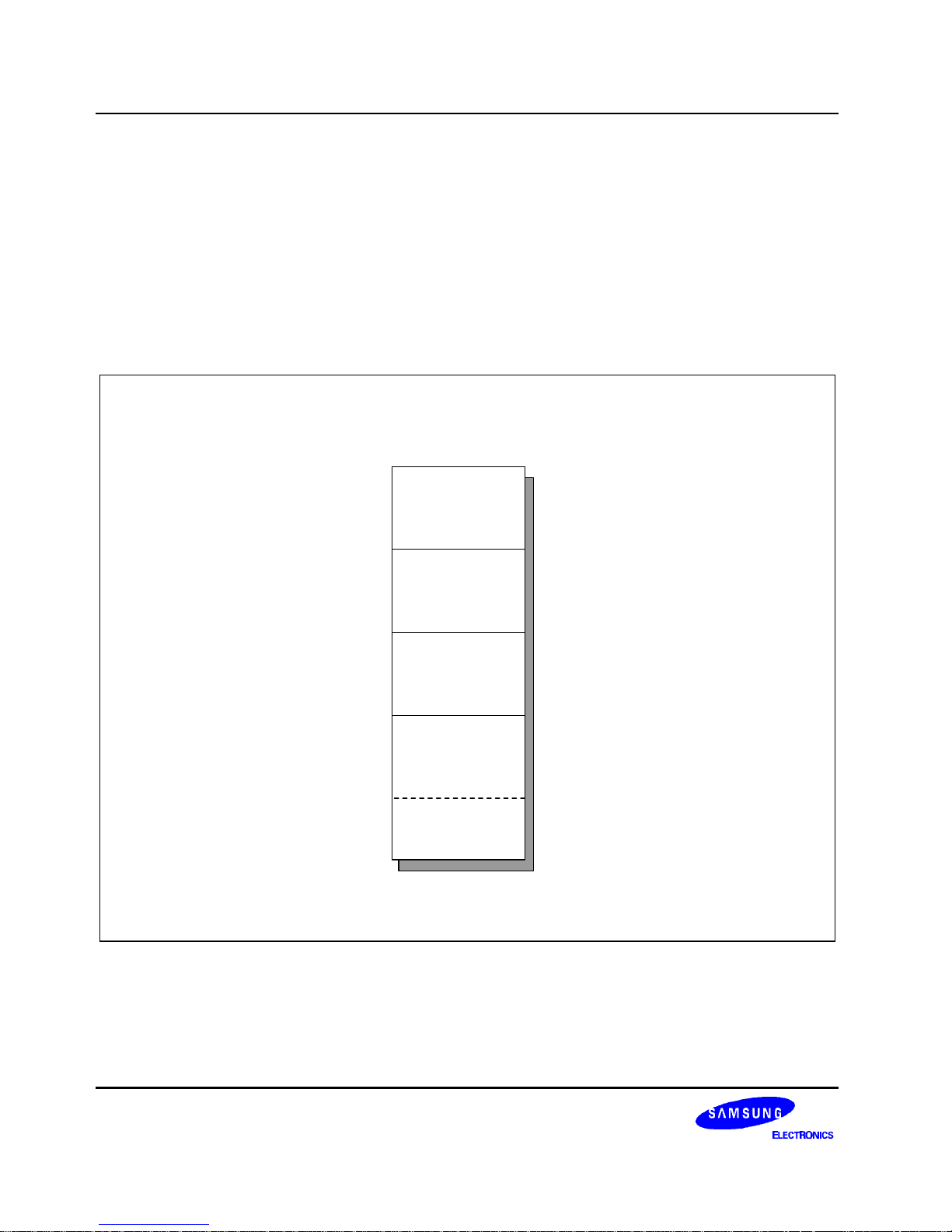
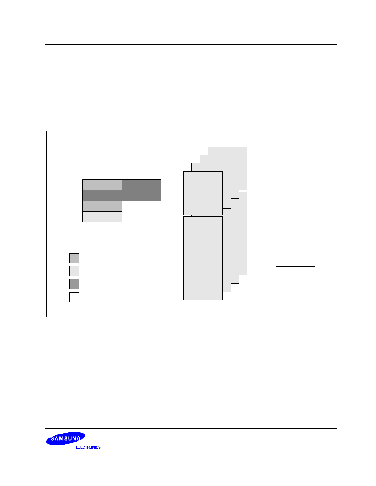
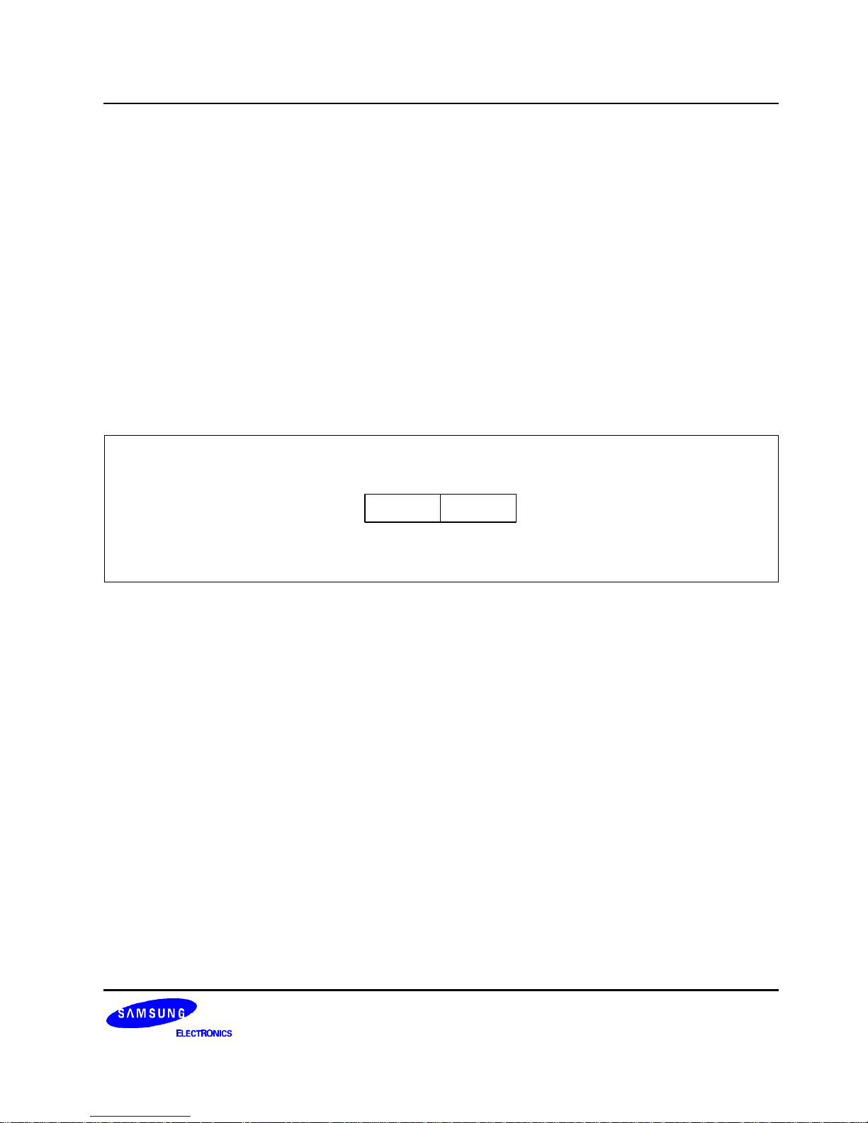
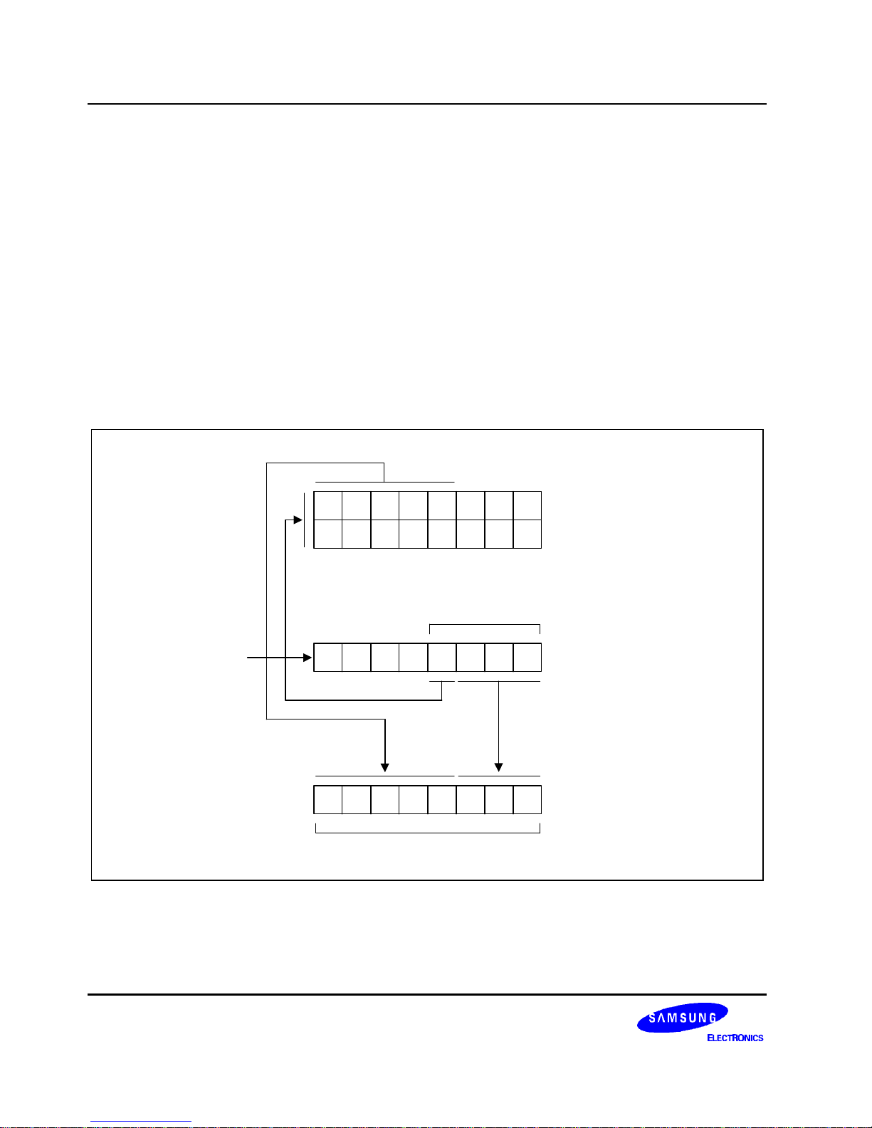
BLOCK DIAGRAM
544/1056 Byte
Register File
OSC/
RESET
Basic
Timer
Watch
Timer
I/O Port and Interrupt Control
16/32-Kbyte
ROM
SAM88 RC CPU
8-Bit
Timer/
Counter B
16-Bit
Timer/
Counter 0
16-Bit
Timer/
Counter 1
I/O Port 0
I/O Port 1
A/D
Converter
I/O Port 2
8-Bit
Timer/
Counter A
I/O Port 3
TAOUT/TAPWM/P3.1
TACLK/P3.2
TACAP/P3.3
TBPWM/P3.0
T1CAP/P1.0
T1CLK/P1.1
T1OUT/T1PWM/P1.2
P0.0-P0.7/
INT0-INT7
P1.0-P1.7
AVREF
AVSS
P2.0-P2.7/
ADC0-ADC7
LCD
Driver
Serial I/O
Port
P3.0-P3.4
Voltage
Detector
VVLDREF
I/O Port 5
I/O Port 4
Voltage
Booster
CB
CA
VLC0-VLC2
COM0-COM3
SEG0-SEG15
SEG16-SEG31
SI/P1.7
SO/P1.5
SCK/P1.6
P4.0-P4.7
P5.0-P5.7
RESET
BUZ/P1.4
XOUT XTOUT
X
IN
XT
IN
Figure 1-1. Block Diagram
PRODUCT OVERVIEW S3C8248/C8245/P8245/C8247/C8249/P8249
1-4
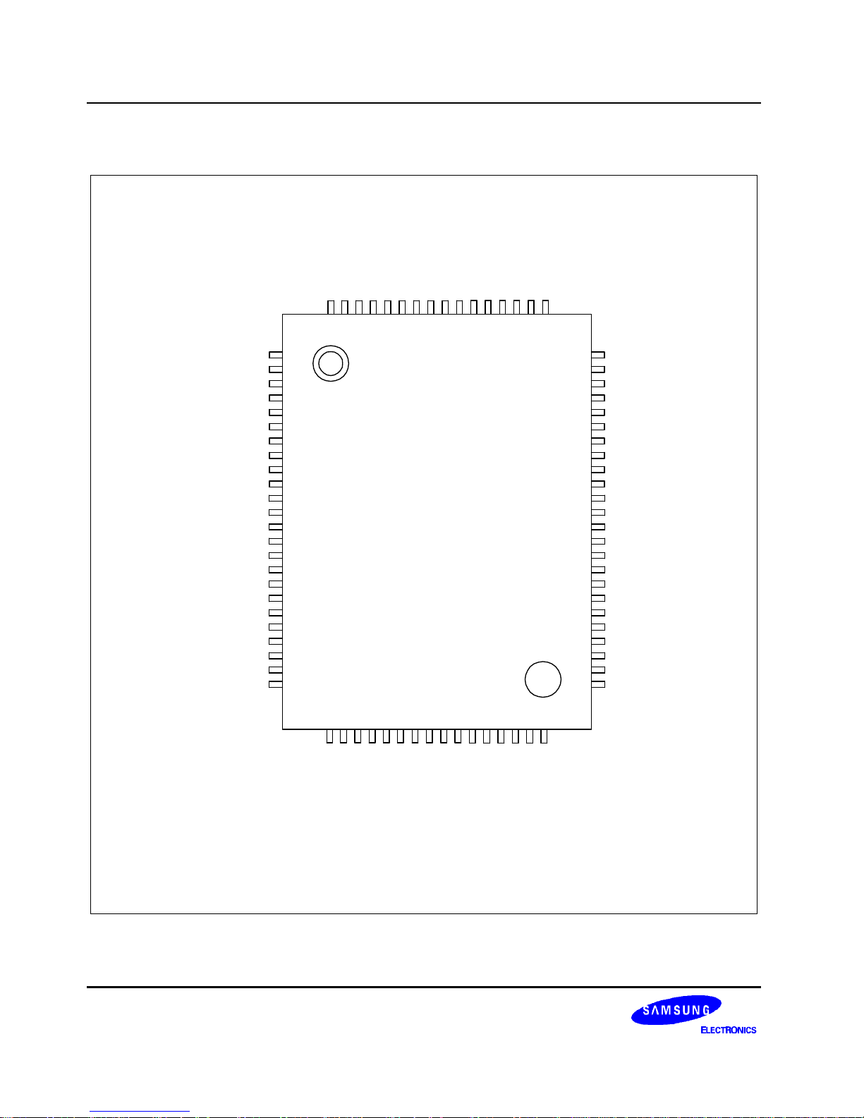
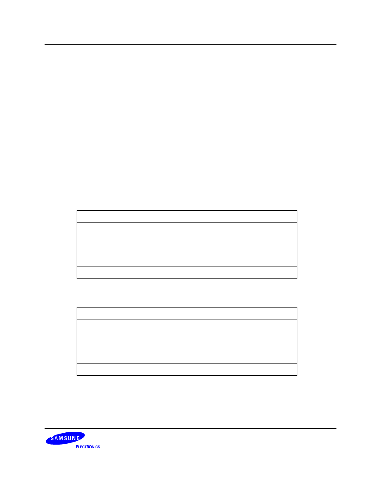
PIN ASSIGNMENT
SEG25/P5.1
SEG24/P5.0
SEG23/P4.7
SEG22/P4.6
SEG21/P4.5
SEG20/P4.4
SEG19/P4.3
SEG18/P4.2
SEG17/P4.1
SEG16/P4.0
SEG15
SEG14
SEG13
SEG12
SEG11
SEG10
SEG26/P5.2
SEG27/P5.3
SEG28/P5.4
SEG29/P5.5
SEG30/P5.6
SEG31/P5.7
P3.0/TBPWM
P3.1/TAOUT/TAPWM
P3.2/TACLK
P3.3/TACAP/SDAT
P3.4/SCLK
VDD
VSS
XOUT
XIN
TEST
XTIN
XTOUT
RESET
P0.0/INT0
P0.1/INT1
P0.2/INT2
P0.3/INT3
P0.4/INT4
S3C8248/C8245
/C8247/C8249
(80-QFP-1420C)
64
63
62
61
60
59
58
57
56
55
54
53
52
51
50
49
48
47
46
45
44
43
42
41
1
2
3
4
5
6
7
8
9
10
11
12
13
14
15
16
17
18
19
20
21
22
23
24
807978777675747372717069686766
65
252627282830313233343536373839
40
SEG9
SEG8
SEG7
SEG6
SEG5
SEG4
SEG3
SEG2
SEG1
SEG0
COM3
COM2
COM1
COM0
VLC2
VLC1
VLC0
CA
CB
AVSS
AVREF
P2.7/ADC7/VVLDREF
P2.6/ADC6
P2.5/ADC5
P0.5/INT5
P0.6/INT6
P0.7/INT7
P1.0/T1CAP
P1.1/T1CLK
P1.2/T1OUT/T1PWM
P1.3
P1.4/BUZ
P1.5/SO
P1.6/SCK
P1.7/SI
P2.0/ADC0
P2.1/ADC1
P2.2/ADC3
P2.3/ADC4
P2.4/ADC4
Figure 1-2. S3C8248/C8245/C8247/C8249 Pin Assignments (80-QFP)
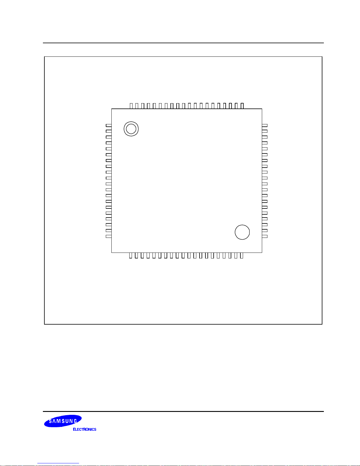
S3C8248/C8245/P8245/C8247/C8249/P8249 PRODUCT OVERVIEW
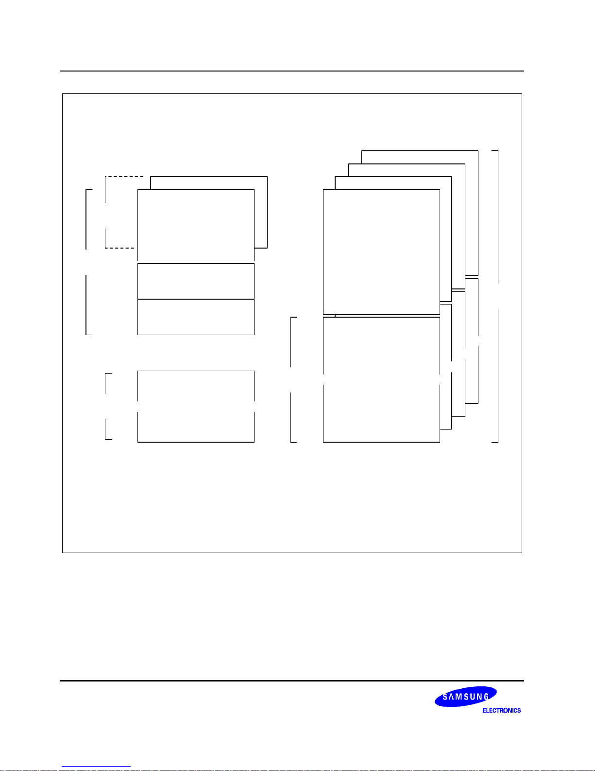
1-5
SEG25/P5.1
SEG24/P5.0
SEG23/P4.7
SEG22/P4.6
SEG21/P4.5
SEG20/P4.4
SEG19/P4.3
SEG18/P4.2
SEG17/P4.1
SEG16/P4.0
SEG15
SEG14
SEG13
SEG12
SEG11
SEG10
SEG9
SEG8
SEG7
SEG6
SEG26/P5.2
SEG27/P5.3
SEG28/P5.4
SEG29/P5.5
SEG30/P5.6
SEG31/P5.7
P3.0/TBPWM
P3.1/TAOUT/TAPWM
P3.2/TACLK
P3.3/TACAP/SDAT
P3.4/SCLK
V
DD
V
SS
X
OUT
X
IN
TEST
XT
IN
XT
OUT
RESET
P0.0/INT0
S3C8248/C8245
/C8247/C8249
(80-TQFP-1212)
60
59
58
57
56
55
54
53
52
51
50
49
48
47
46
45
44
43
42
41
1
2
3
4
5
6
7
8
9
10
11
12
13
14
15
16
17
18
19
20
80797877767574737271706968676665646362
61
21222324252627282830313233343536373839
40
SEG5
SEG4
SEG3
SEG2
SEG1
SEG0
COM3
COM2
COM1
COM0
V
LC2
V
LC1
V
LC0
CA
CB
AV
SS
AV
REF
P2.7/ADC7/V
LDREF
P2.6/ADC6
P2.5/ADC5
P0.1/INT1
P0.2/INT2
P0.3/INT3
P0.4/INT4
P0.5/INT5
P0.6/INT6
P0.7/INT7
P1.0/T1CAP
P1.1/T1CLK
P1.2/T1OUT/T1PWM
P1.3
P1.4/BUZ
P1.5/SO
P1.6/SCK
P1.7/SI
P2.0/ADC0
P2.1/ADC1
P2.2/ADC3
P2.3/ADC4
P2.4/ADC4
Figure 1-3. S3C8248/C8245/C8247/C8249 Pin Assignments (80-TQFP)
PRODUCT OVERVIEW S3C8248/C8245/P8245/C8247/C8249/P8249
1-6
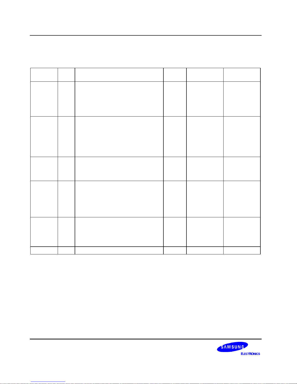
PIN DESCRIPTIONS
Table 1-1. S3C8248/C8245/C8247/C8249 Pin Descriptions
Pin
Names
Pin
Type
Pin
Description
Circuit
Type
Pin
Numbers
(note)
Share
Pins
P0.0–P0.7 I/O I/O port with bit programmable pins;
Schmitt trigger input or output mode
selected by software; software assignable
pull-up. P0.0–P0.7 can be used as inputs
for external interrupts INT0–INT7
(with noise filter and interrupt control).
D–4 20–27 INT0–INT7
P1.0–1.7 I/O I/O port with bit programmable pins; Input
or output mode selected by software;
Open-drain output mode can be selected
by software; software assignable pull-up.
Alternately P1.0–P1.7 can be used as SI,
SO, SCK, BUZ, T1CAP, T1CLK, T1OUT,
T1PWM
E–2 28-35 SI, SO, SCK,
BUZ, T1CAP
T1CLK
T1OUT
T1PWM
P2.0–P2.7 I/O I/O port with bit programmable pins;
normal input and AD input or output
mode selected by software; software
assignable pull-up.
F–10
F–18
36–42,
43
ADC0–ADC6
V
VLDREF
(ADC7)
P3.0–P3.4 I/O I/O port with bit programmable pins. Input
or push-pull output with software
assignable pull-up. Alternately P3.0–P3.3
can be used as TACAP, TACLK, TAOUT,
TAPWM, TBPWM
D–2 7–11 TACAP
TACLK
TAOUT
TAPWM
TBPWM
P4.0–P4.7 I/O I/O port with bit programmable pins.
Push-pull or open drain output and input
with software assignable pull-up.
P4.0–P4.7 can alternately be used as
outputs for LCD SEG
H–14 71–78 SEG16–SEG23
P5.0–P5.7 I/O Have the same characteristic as port 4 H–14 79–6 SEG24–SEG31
S3C8248/C8245/P8245/C8247/C8249/P8249 PRODUCT OVERVIEW
1-7
Table 1-1. S3C8248/C8245/C8247/C8249 Pin Descriptions (Continued)
Pin
Names
Pin
Type
Pin
Description
Circuit
Type
Pin
Numbers
(note)
Share
Pins
ADC0–ADC6
ADC7
I A/D converter analog input channels F–10
F–18
36–42
43
P2.0–P2.6
P2.7
AV
REF
– A/D converter reference voltage – 44 –
AV
SS
– A/D converter ground – 45 –
INT0–INT7 I External interrupt input pins D–4 20–27 P0.0–P0.7
RESET
I System reset pin
(pull-up resistor: 250 kΩ)
B 19 –
TEST I 0 V: Normal MCU operating
5 V: Test mode
12 V: for OTP writing
– 16 –
SDAT, SCLK O Serial OTP interface pins; serial data
and clock
D–2 10, 11 P3.3, P3.4
V
DD, VSS
– Power input pins for CPU operation
(internal) and Power input for OTP
Writing
– 12, 13 –
X
OUT, XIN
– Main oscillator pins – 14, 15 –
SCK, SO, SI I/O Serial I/O interface clock signal E–2 33–35 P1.5–P1.7
V
VLDREF
I Voltage detector reference voltage
input
F–18 43 P2.7
TACAP I Timer A Capture input D–2 10 P3.3
TACLK I Timer A External clock input D–2 9 P3.2
TAOUT/TAPWM O Timer A output and PWM output D–2 8 P3.1
TBPWM O Timer B PWM output D–2 7 P3.0
T1CAP I Timer 1 Capture input E–2 28 P1.0
T1CLK I Timer 1 External clock input E–2 29 P1.1
T1OUT/T1PWM O Timer 1 output and PWM output E–2 30 P1.2
COM0–COM3 O LCD common signal output H 51–54 –
SEG0–SEG15 O LCD segment output H 55–70 –
SEG16–SEG23 O LCD segment output H–14 71–78 P4.0–P4.7
SEG24–SEG31 O LCD Segment output H–14 79–6 P5.0–P5.7
V
LC0–VLC2
O LCD power supply – 48–50 –
BUZ O 0.5, 1, 2 or 4 kHz frequency output for
buzzer sound with 4.19 MHz main
system clock or 32768 Hz subsystem
clock
E–2 32 P1.4
CA, CB – Capacitor terminal for voltage booster – 46–47 –
PRODUCT OVERVIEW S3C8248/C8245/P8245/C8247/C8249/P8249
1-8
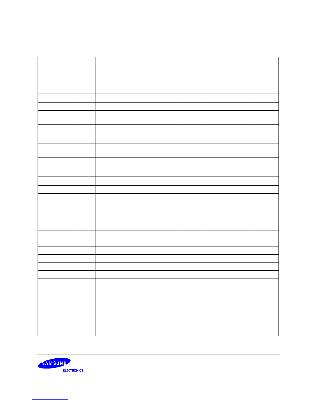
PIN CIRCUITS
In
VDD
Figure 1-4. Pin Circuit Type B (RESETRESET)
P-Channel
N-Channel
V
DD
Out
Output
Disable
Data
Figure 1-5. Pin Circuit Type C
P-Channel
I/O
Output
Disable
Data
Circuit
Type C
Pull-up
Enable
VDD
Figure 1-6. Pin Circuit Type D-2 (P3)
I/O
Output
Disable
Data
Pin Circuit
Type C
Pull-up
Enable
VDD
Noise
Filter
Ext.INT
Input
Normal
VDD
Figure 1-7. Pin Circuit Type D-4 (P0)
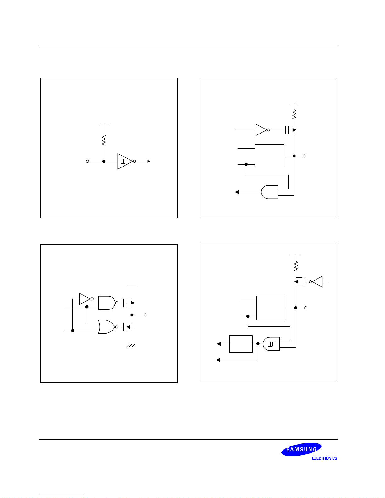
S3C8248/C8245/P8245/C8247/C8249/P8249 PRODUCT OVERVIEW
1-9
VDD
Output
Disable
Data
Pull-up
Resistor
VDD
I/O
P-CH
N-CH
Schmitt Trigger
Open drain
Enable
Figure 1-8. Pin Circuit Type E-2 (P1)
Pull-up
Enable
Circuit
Type C
Data
Output
Disable
ADCEN
To ADC
Data
VDD
I/O
Figure 1-9. Pin Circuit Type F-10 (P2.0–P2.6)
Pull-up
Enable
Circuit
Type C
Data
Output
Disable
ADC & VLD
Enable
Data
To ADC
VLDREF
I/O
VDD
Figure 1-10. Pin Circuit Type F-18 (P2.7/VLD
REF
)
Out
VLC1
SEG/
COM
VLC0
VLC2
Figure 1-11. Pin Circuit Type H (SEG/COM)
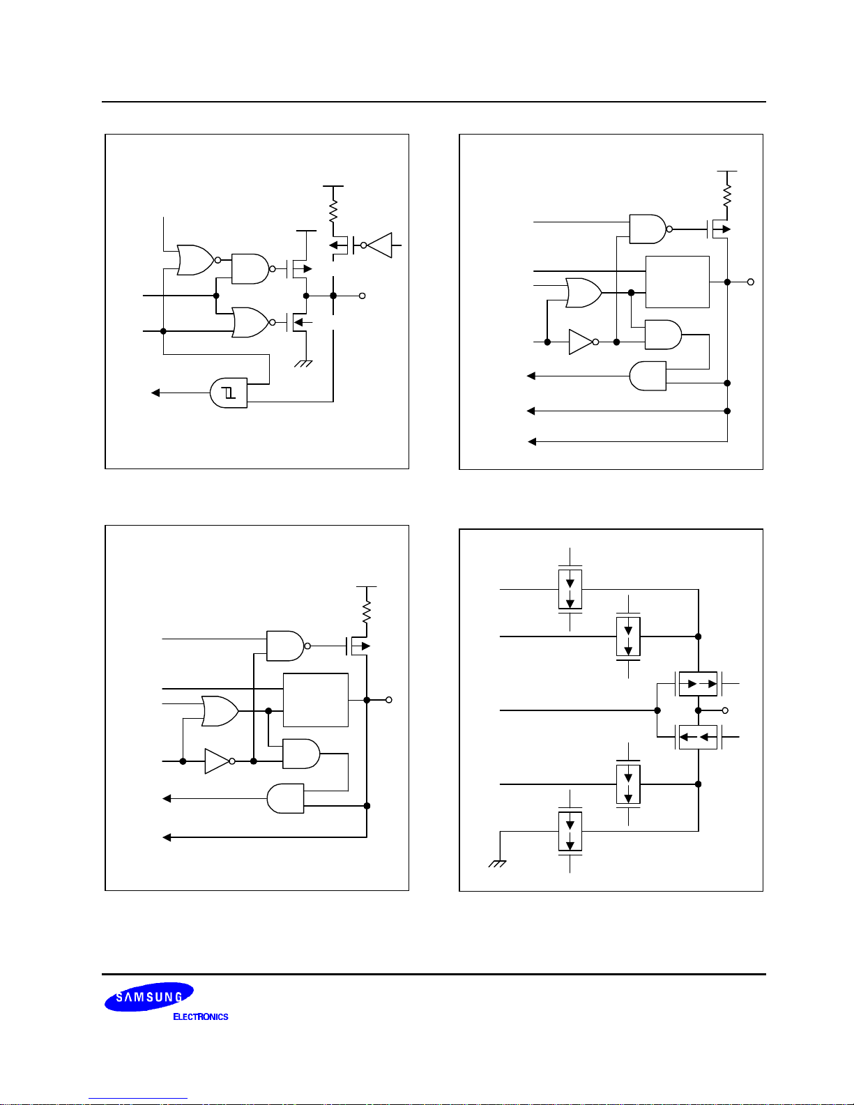
PRODUCT OVERVIEW S3C8248/C8245/P8245/C8247/C8249/P8249
1-10
SEG
VLC2
VLC1
VLC0
Output
Disable
Figure 1-12. Pin Circuit Type H-4
VDD
Open Drain EN
Data
LCD Out EN
SEG
Output
Disable
Pull-up
Enable
VDD
Circuit
Type H-4
Figure 1-13. Pin Circuit Type H-14 (P4, P5)

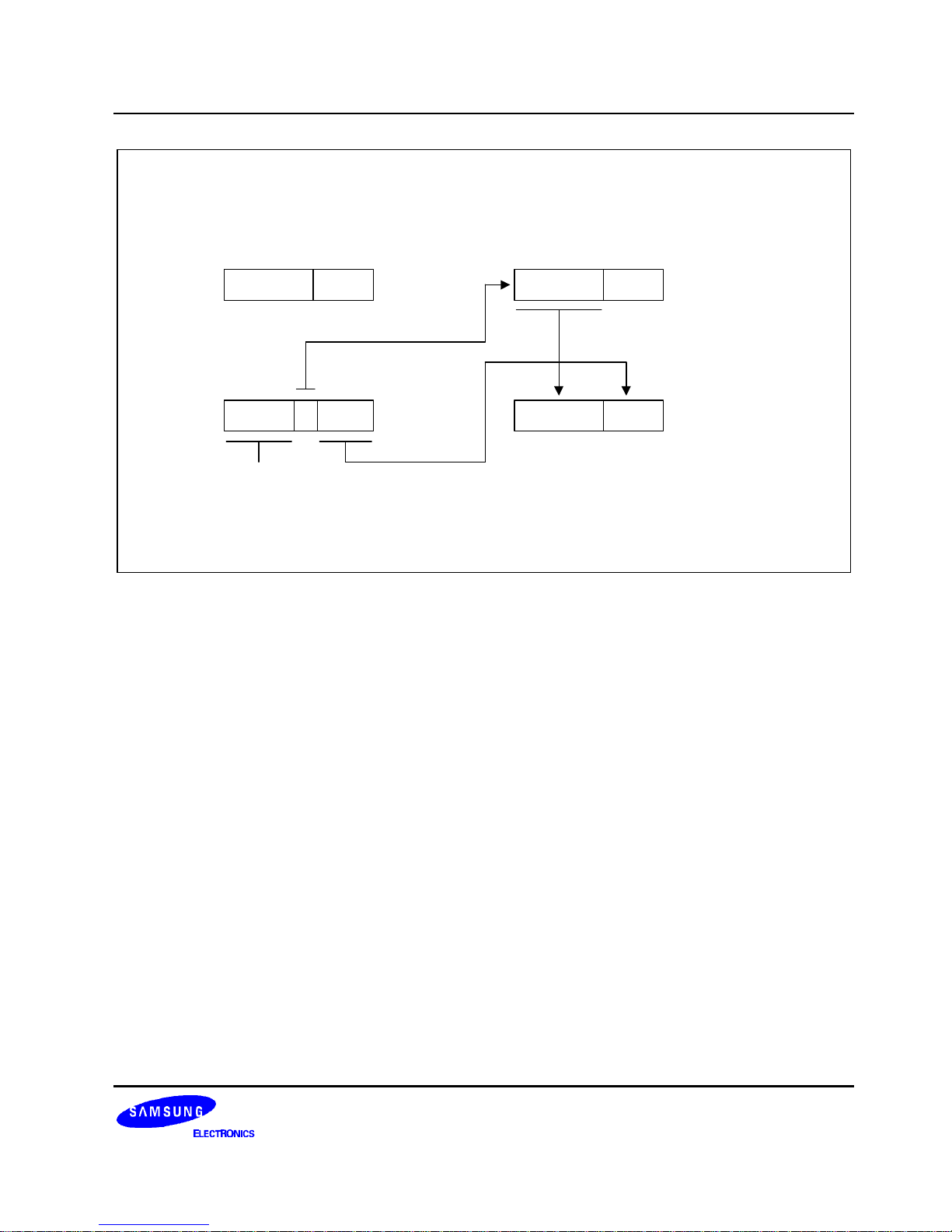
S3C8248/C8245/P8245/C8247/C8249/P8249 ADDRESS SPACES
2-1
2 ADDRESS SPACES
OVERVIEW
The S3C8248/C8245/C8247/C8249 microcontroller has two types of address space:
— Internal program memory (ROM)
— Internal register file
A 16-bit address bus supports program memory operations. A separate 8-bit register bus carries addresses and
data between the CPU and the register file.
The S3C8248/C8245 has an internal 16-Kbyte mask-programmable ROM. The S3C8247/C8249 has an internal
32-Kbyte mask-programmable ROM.
The 256-byte physical register space is expanded into an addressable area of 320 bytes using addressing modes.
A 16-byte LCD display register file is implemented.
There are 1,109 mapped registers in the internal register file. Of these, 1,040 are for general-purpose.
(This number includes a 16-byte working register common area used as a “scratch area” for data operations, four
192-byte prime register areas, and four 64-byte areas (Set 2)). Thirteen 8-bit registers are used for the CPU and
the system control, and 53 registers are mapped for peripheral controls and data registers. Twelve register
locations are not mapped.
ADDRESS SPACES S3C8248/C8245/P8245/C8247/C8249/P8249
2-2
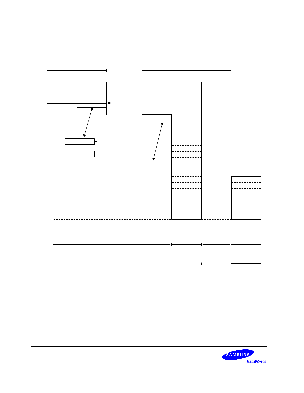
PROGRAM MEMORY (ROM)
Program memory (ROM) stores program codes or table data. The S3C8248 has 8K bytes internal maskprogrammable program memory, the S3C8245 has 16K bytes, the S3C8247 has 24K bytes and the S3C8249 has
32K bytes.
The first 256 bytes of the ROM (0H–0FFH) are reserved for interrupt vector addresses. Unused locations in this
address range can be used as normal program memory. If you use the vector address area to store a program
code, be careful not to overwrite the vector addresses stored in these locations.
The ROM address at which a program execution starts after a reset is 0100H.
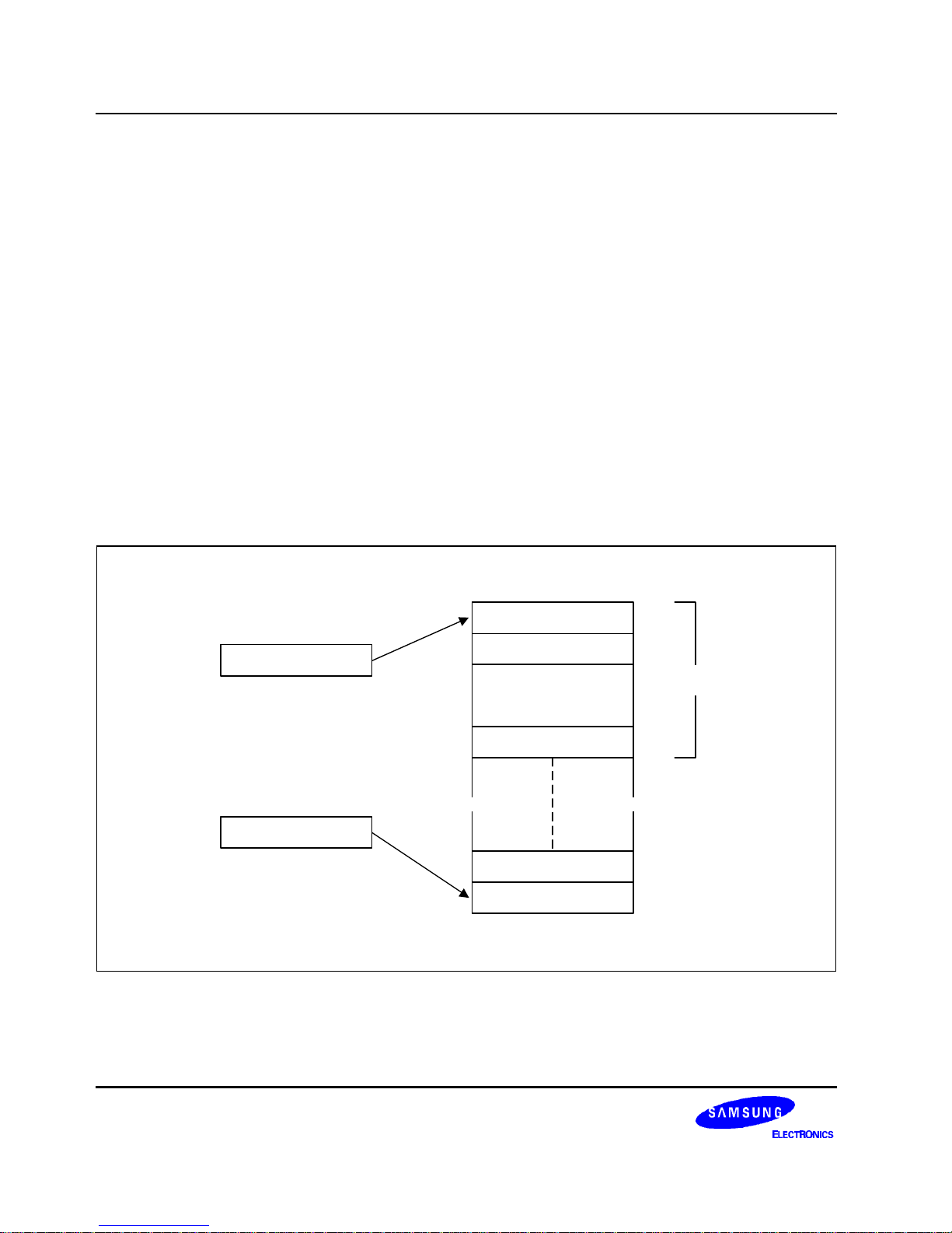
(Decimal)
32,767
255
(HEX)
7FFFH (S3C8249)
0FFH
0H
0
Interrupt
Vector Area
32K-byte
3FFFH (S3C8245)
4000H
16383
16384
16K-byte
5FFFH (S3C8247)
6000H
24K-byte
1FFFH (S3C8248)
2000H
8K-byte
Figure 2-1. Program Memory Address Space
S3C8248/C8245/P8245/C8247/C8249/P8249 ADDRESS SPACES
2-3
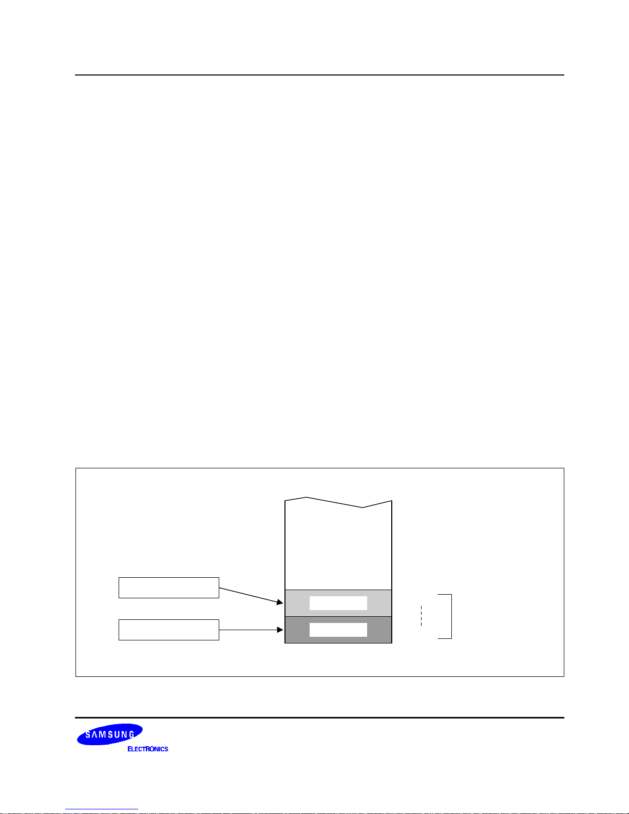
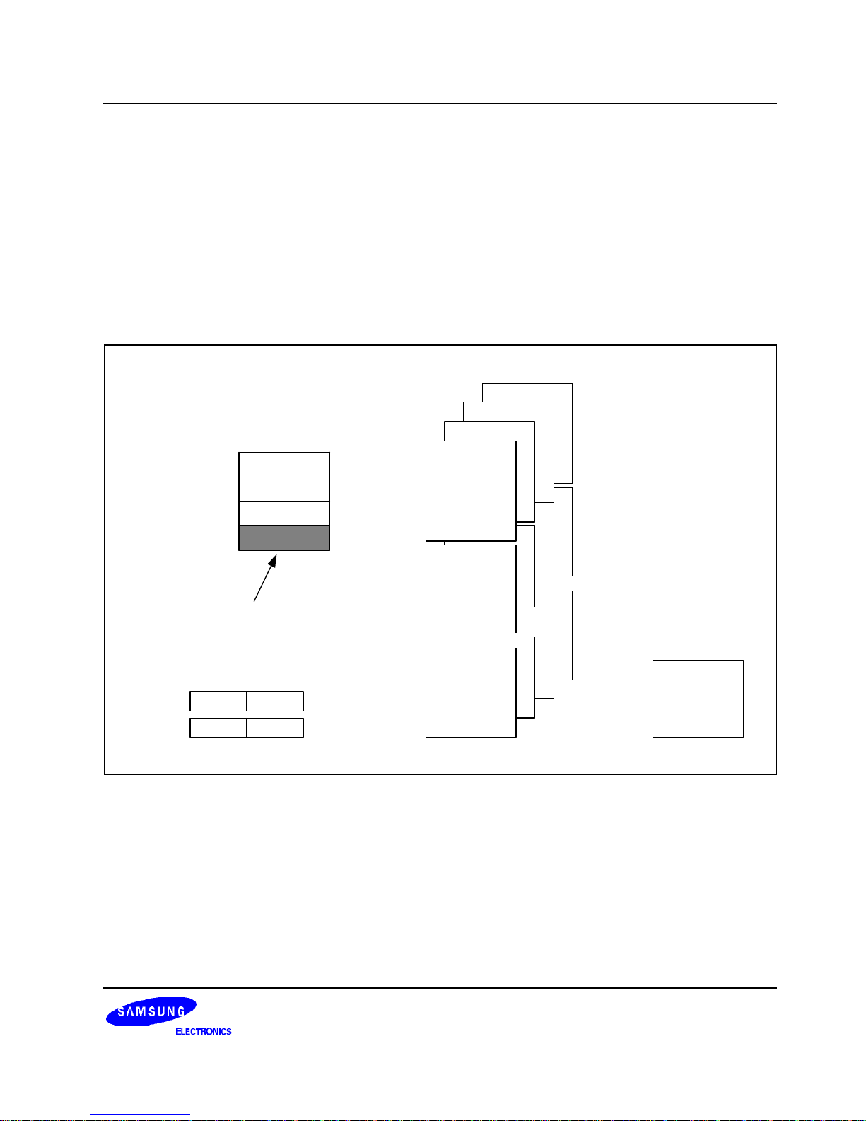
REGISTER ARCHITECTURE
In the S3C8248/C8245/C8247/C8249 implementation, the upper 64-byte area of register files is expanded two
64-byte areas, called set 1 and set 2. The upper 32-byte area of set 1 is further expanded two 32-byte register
banks (bank 0 and bank 1), and the lower 32-byte area is a single 32-byte common area.
In case of S3C8247/C8249/P8249 the total number of addressable 8-bit registers is 1122. Of these 1122
registers, 16 bytes are for CPU and system control registers, 16 bytes are for LCD data registers, 50 bytes are for
peripheral control and data registers, 16 bytes are used as a shared working registers, and 1024 registers are for
general-purpose use, page 0-page 4 (in case of S3C8248/C8245/P8245, page 0-page 2).
You can always address set 1 register locations, regardless of which of the four register pages is currently
selected. Set 1 locations, however, can only be addressed using register addressing modes.
The extension of register space into separately addressable areas (sets, banks, and pages) is supported by
various addressing mode restrictions, the select bank instructions, SB0 and SB1, and the register page pointer
(PP).
Specific register types and the area (in bytes) that they occupy in the register file are summarized in Table 2–1.
Table 2-1. S3C8247/C8249/P8249 Register Type Summary
Register Type Number of Bytes
General-purpose registers (including the 16-byte
common working register area, four 192-byte prime
register area, and four 64-byte set 2 area)
LCD data registers
CPU and system control registers
Mapped clock, peripheral, I/O control, and data registers
1,040
16
16
50
Total Addressable Bytes
1,122
Table 2-2. S3C8248/C8245/P8245 Register Type Summary
Register Type Number of Bytes
General-purpose registers (including the 16-byte
common working register area, four 192-byte prime
register area, and four 64-byte set 2 area)
LCD data registers
CPU and system control registers
Mapped clock, peripheral, I/O control, and data registers
528
16
16
50
Total Addressable Bytes
610
ADDRESS SPACES S3C8248/C8245/P8245/C8247/C8249/P8249
2-4
System Registers
(Register Addressing Mode)
General Purpose Register
(Register Addressing Mode)
Bank 1
System and
Peripheral Control
Registers
Bank 0
System and
Peripheral Control
Registers
(Register Addressing Mode)
Set1
FFH
E0H
32
Bytes
E0H
DFH
D0H
CFH
C0H
Prime
Data Registers
(All addressing modes)
LCD Display Reigster
~ ~
Page 4
0FH
00H
16
Bytes
~
Page 1
~
Page3
~
Page 2
~
Page 1
Page 0
Prime
Data Registers
(All Addressing Modes)
Page 0
Set 2
General-Purpose
Data Registers
(Indirect Register, Indexed
Mode, and Stack
Operations)
~ ~
~
C0H
BFH
00H
FFH
FFH
FFH
FFH
192
Bytes
64
Bytes
256
Bytes
NOTE: In case of S3C8248/C8245/P8245, there are page 0, page 1, and page 2.
Page 2 is for LCD display register, 16 bytes.
Figure 2-2. Internal Register File Organization
S3C8248/C8245/P8245/C8247/C8249/P8249 ADDRESS SPACES
2-5
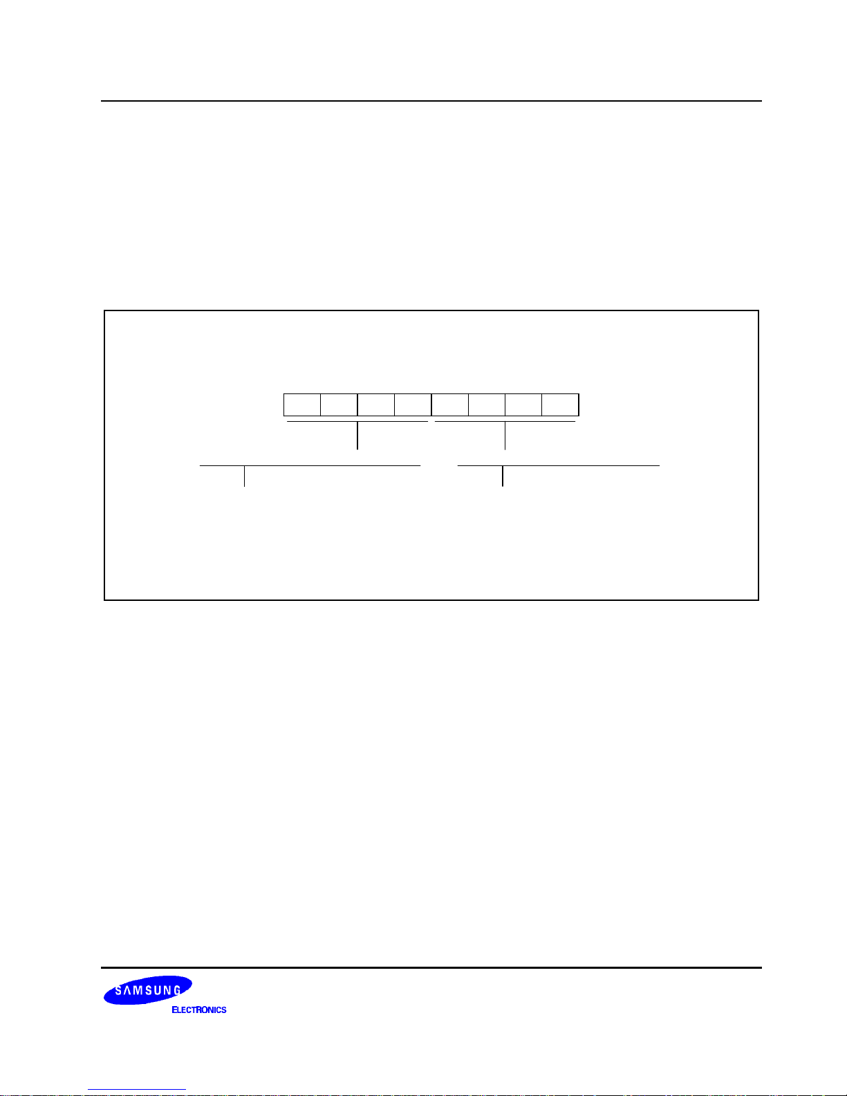
REGISTER PAGE POINTER (PP)
The S3C8-series architecture supports the logical expansion of the physical 256-byte internal register file (using
an 8-bit data bus) into as many as 16 separately addressable register pages. Page addressing is controlled by the
register page pointer (PP, DFH). In the S3C8248/C8245/C8247/C8249 microcontroller, a paged register file
expansion is implemented for LCD data registers, and the register page pointer must be changed to address
other pages.
After a reset, the page pointer's source value (lower nibble) and the destination value (upper nibble) are always
"0000", automatically selecting page 0 as the source and destination page for register addressing.
Register Page Pointer (PP)
DFH ,Set 1, R/W
LSBMSB .7 .6 .5 .4 .3 .2 .1 .0
Destination register page selection bits:
0000 Destination: Page 0
Source register page selection bits:
0000 Source: Page 0
NOTE: A hardware reset operation writes the 4-bit destination and
source values shown above to the register page pointer. These values should
be modified to address other pages.
Figure 2-3. Register Page Pointer (PP)
++ PROGRAMMING TIP — Using the Page Pointer for RAM clear (Page 0, Page 1)
LD PP,#00H ; Destination ← 0, Source ← 0
SRP #0C0H
LD R0,#0FFH ; Page 0 RAM clear starts
RAMCL0 CLR @R0
DJNZ R0,RAMCL0
CLR @R0 ; R0 = 00H
LD PP,#10H ; Destination ← 1, Source ← 0
LD R0,#0FFH ; Page 1 RAM clear starts
RAMCL1 CLR @R0
DJNZ R0,RAMCL1
CLR @R0 ; R0 = 00H
NOTE: You should refer to page 6-39 and use DJNZ instruction properly when DJNZ instruction is used in your program.

ADDRESS SPACES S3C8248/C8245/P8245/C8247/C8249/P8249
2-6
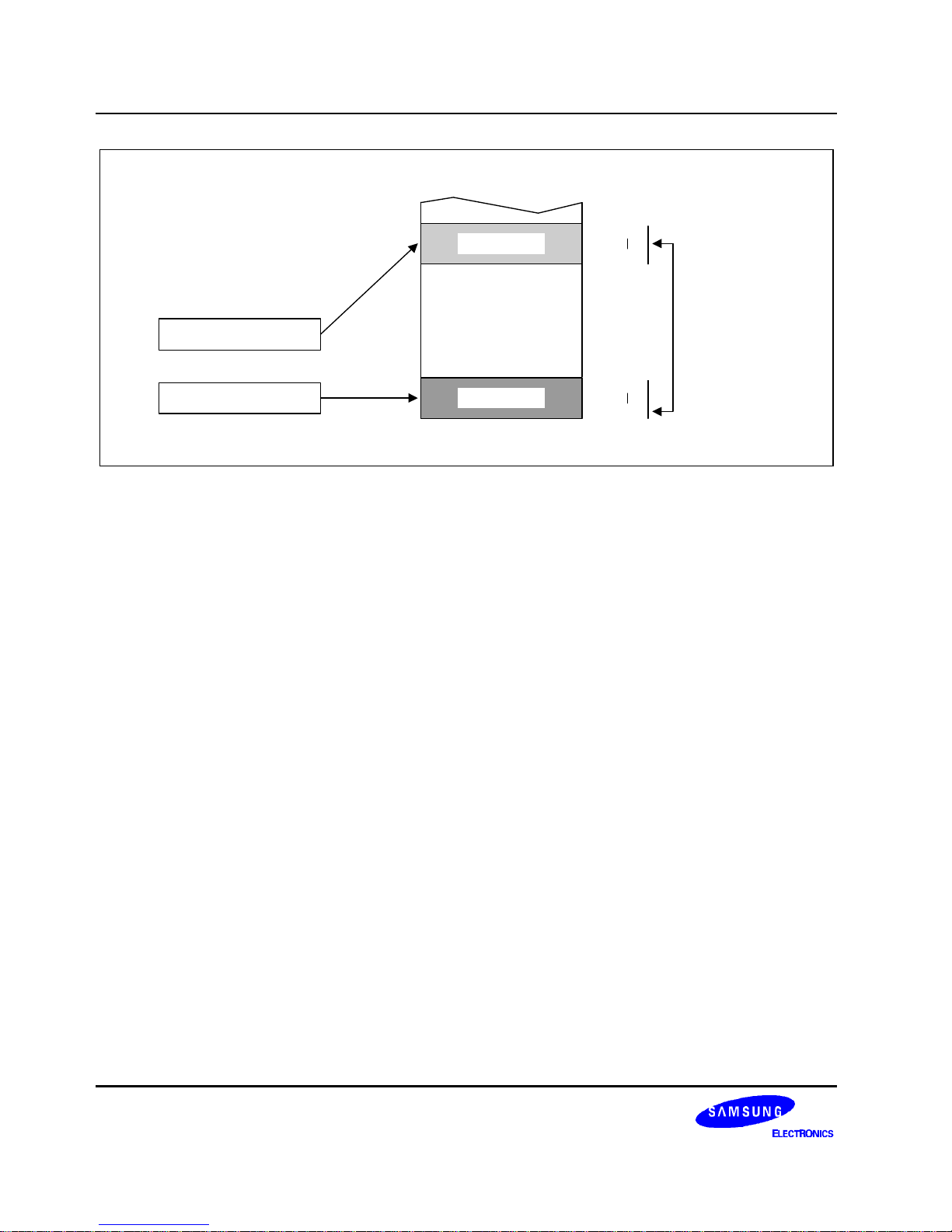
REGISTER SET 1
The term set 1 refers to the upper 64 bytes of the register file, locations C0H–FFH.
The upper 32-byte area of this 64-byte space (E0H–FFH) is expanded two 32-byte register banks, bank 0 and
bank 1. The set register bank instructions, SB0 or SB1, are used to address one bank or the other. A hardware
reset operation always selects bank 0 addressing.
The upper two 32-byte areas (bank 0 and bank 1) of set 1 (E0H–FFH) contains 50 mapped system and
peripheral control registers. The lower 32-byte area contains 16 system registers (D0H–DFH) and a 16-byte
common working register area (C0H–CFH). You can use the common working register area as a “scratch” area
for data operations being performed in other areas of the register file.
Registers in set 1 locations are directly accessible at all times using Register addressing mode. The 16-byte
working register area can only be accessed using working register addressing (For more information about
working register addressing, please refer to Chapter 3, “Addressing Modes.”)
REGISTER SET 2
The same 64-byte physical space that is used for set 1 locations C0H–FFH is logically duplicated to add another
64 bytes of register space. This expanded area of the register file is called set 2. For the S3C8247/C8249,
the set 2 address range (C0H–FFH) is accessible on pages 0–3.
S3C8248/C8245, the set 2 address range (C0H-FFH) is accessible on pages 0-1.
The logical division of set 1 and set 2 is maintained by means of addressing mode restrictions. You can use only
Register addressing mode to access set 1 locations. In order to access registers in set 2, you must use Register
Indirect addressing mode or Indexed addressing mode.
The set 2 register area is commonly used for stack operations.
S3C8248/C8245/P8245/C8247/C8249/P8249 ADDRESS SPACES
2-7
PRIME REGISTER SPACE
The lower 192 bytes (00H–BFH) of the S3C8248/C8245/C8247/C8249's four or two 256-byte register pages is
called prime register area. Prime registers can be accessed using any of the seven addressing modes
(see Chapter 3, "Addressing Modes.")
The prime register area on page 0 is immediately addressable following a reset. In order to address prime
registers on pages 0, 1, 2, 3, or 4 you must set the register page pointer (PP) to the appropriate source and
destination values.
FFH
FCH
E0H
D0H
C0H
Set 1
Bank 0
Peripheral and I/O
General-purpose
CPU and system control
LCD data register
FFH
Page 3
Set 2
FFH
Page 2
Set 2
FFH
Page 1
Set 2
FFH
C0H
00H
BFH
Page 0
Set 2
Page 0
Prime
Space
LCD Data
Register Area
Page 4
00H
0FH
Bank 1
Figure 2-4. Set 1, Set 2, Prime Area Register, and LCD Data Register Map
ADDRESS SPACES S3C8248/C8245/P8245/C8247/C8249/P8249
2-8
WORKING REGISTERS
Instructions can access specific 8-bit registers or 16-bit register pairs using either 4-bit or 8-bit address fields.
When 4-bit working register addressing is used, the 256-byte register file can be seen by the programmer as one
that consists of 32 8-byte register groups or "slices." Each slice comprises of eight 8-bit registers.
Using the two 8-bit register pointers, RP1 and RP0, two working register slices can be selected at any one time to
form a 16-byte working register block. Using the register pointers, you can move this 16-byte register block
anywhere in the addressable register file, except the set 2 area.
The terms slice and block are used in this manual to help you visualize the size and relative locations of selected
working register spaces:
— One working register slice is 8 bytes (eight 8-bit working registers, R0–R7 or R8–R15)
— One working register block is 16 bytes (sixteen 8-bit working registers, R0–R15)
All the registers in an 8-byte working register slice have the same binary value for their five most significant
address bits. This makes it possible for each register pointer to point to one of the 24 slices in the register file.
The base addresses for the two selected 8-byte register slices are contained in register pointers RP0 and RP1.
After a reset, RP0 and RP1 always point to the 16-byte common area in set 1 (C0H–CFH).
Each register pointer points to
one 8-byte slice of the register
space, selecting a total 16-byte
working register block.
1 1 1 1 1 X X X
RP1 (Registers R8-R15)
RP0 (Registers R0-R7)
Slice 32
Slice 31
~ ~
CFH
C0H
FFH
F8H
F7H
F0H
FH
8H
7H
0H
Slice 2
Slice 1
10H
Set 1
Only
0 0 0 0 0 X X X
Figure 2-5. 8-Byte Working Register Areas (Slices)
S3C8248/C8245/P8245/C8247/C8249/P8249 ADDRESS SPACES
2-9
USING THE REGISTER POINTS
Register pointers RP0 and RP1, mapped to addresses D6H and D7H in set 1, are used to select two movable
8-byte working register slices in the register file. After a reset, they point to the working register common area:
RP0 points to addresses C0H–C7H, and RP1 points to addresses C8H–CFH.
To change a register pointer value, you load a new value to RP0 and/or RP1 using an SRP or LD instruction.
(see Figures 2-6 and 2-7).
With working register addressing, you can only access those two 8-bit slices of the register file that are currently
pointed to by RP0 and RP1. You cannot, however, use the register pointers to select a working register space in
set 2, C0H–FFH, because these locations can be accessed only using the Indirect Register or Indexed
addressing modes.
The selected 16-byte working register block usually consists of two contiguous 8-byte slices. As a general
programming guideline, it is recommended that RP0 point to the "lower" slice and RP1 point to the "upper" slice
(see Figure 2-6). In some cases, it may be necessary to define working register areas in different (noncontiguous) areas of the register file. In Figure 2-7, RP0 points to the "upper" slice and RP1 to the "lower" slice.
Because a register pointer can point to either of the two 8-byte slices in the working register block, you can
flexibly define the working register area to support program requirements.
++ PROGRAMMING TIP — Setting the Register Pointers
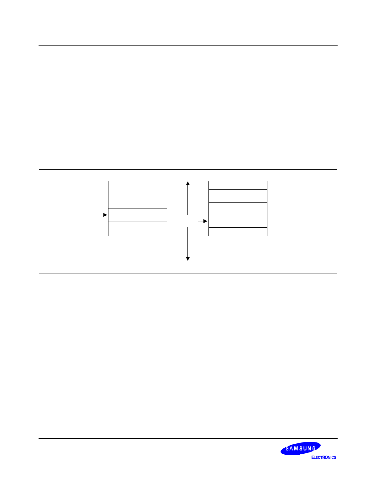
SRP #70H ; RP0 ← 70H, RP1 ← 78H
SRP1 #48H ; RP0 ← no change, RP1 ← 48H,
SRP0 #0A0H ; RP0 ← A0H, RP1 ← no change
CLR RP0 ; RP0 ← 00H, RP1 ← no change
LD RP1,#0F8H ; RP0 ← no change, RP1 ← 0F8H
FH (R15)
0H (R0)
16-Byte
Contiguous
Working
Register block
Register File
Contains 32
8-Byte Slices
RP0
RP1
8H
7H
0 0 0 0 1 X X X
0 0 0 0 0 X X X
8-Byte Slice
8-Byte Slice
Figure 2-6. Contiguous 16-Byte Working Register Block
ADDRESS SPACES S3C8248/C8245/P8245/C8247/C8249/P8249
2-10
16-Byte
Contiguous
working
Register block
Register File
Contains 32
8-Byte Slices
0 0 0 0 0 X X X
RP1
1 1 1 1 0 X X X
RP0
0H (R0)
7H (R15)
F0H (R0)
F7H (R7)
8-Byte Slice
8-Byte Slice
Figure 2-7. Non-Contiguous 16-Byte Working Register Block
++ PROGRAMMING TIP — Using the RPs to Calculate the Sum of a Series of Registers
Calculate the sum of registers 80H–85H using the register pointer. The register addresses from 80H through 85H
contain the values 10H, 11H, 12H, 13H, 14H, and 15 H, respectively:
SRP0 #80H ; RP0 ← 80H
ADD R0,R1 ; R0 ← R0 + R1
ADC R0,R2 ; R0 ← R0 + R2 + C
ADC R0,R3 ; R0 ← R0 + R3 + C
ADC R0,R4 ; R0 ← R0 + R4 + C
ADC R0,R5 ; R0 ← R0 + R5 + C
The sum of these six registers, 6FH, is located in the register R0 (80H). The instruction string used in this
example takes 12 bytes of instruction code and its execution time is 36 cycles. If the register pointer is not used
to calculate the sum of these registers, the following instruction sequence would have to be used:
ADD 80H,81H ; 80H ← (80H) + (81H)
ADC 80H,82H ; 80H ← (80H) + (82H) + C
ADC 80H,83H ; 80H ← (80H) + (83H) + C
ADC 80H,84H ; 80H ← (80H) + (84H) + C
ADC 80H,85H ; 80H ← (80H) + (85H) + C
Now, the sum of the six registers is also located in register 80H. However, this instruction string takes 15 bytes of
instruction code rather than 12 bytes, and its execution time is 50 cycles rather than 36 cycles.
S3C8248/C8245/P8245/C8247/C8249/P8249 ADDRESS SPACES
2-11
REGISTER ADDRESSING
The S3C8-series register architecture provides an efficient method of working register addressing that takes full
advantage of shorter instruction formats to reduce execution time.
With Register (R) addressing mode, in which the operand value is the content of a specific register or register
pair, you can access any location in the register file except for set 2. With working register addressing, you use a
register pointer to specify an 8-byte working register space in the register file and an 8-bit register within that
space.
Registers are addressed either as a single 8-bit register or as a paired 16-bit register space. In a 16-bit register
pair, the address of the first 8-bit register is always an even number and the address of the next register is always
an odd number. The most significant byte of the 16-bit data is always stored in the even-numbered register, and
the least significant byte is always stored in the next (+1) odd-numbered register.
Working register addressing differs from Register addressing as it uses a register pointer to identify a specific
8-byte working register space in the internal register file and a specific 8-bit register within that space.
MSB
Rn
LSB
Rn+1
n = Even address
Figure 2-8. 16-Bit Register Pair
ADDRESS SPACES S3C8248/C8245/P8245/C8247/C8249/P8249
2-12
RP1
RP0
Register
Pointers
00H
All
Addressing
Modes
Page 0
Indirect Register,
Indexed
Addressing
Modes
Page 0
Register Addressing Only
Can be Pointed by Register Pointer
FFH
E0H
BFH
Control
Registers
System
Registers
Special-Purpose Registers
D0H
C0H
Bank 1 Bank 1
NOTE: In the S3C8248/C8245/C8247/C8249
microcontroller, pages 0-4 are implemented.
Pages 0-4 contain all of the addressable
registers in the internal register file.
Each register pointer (RP) can independently point
to one of the 24 8-byte "slices" of the register file
(other than set 2). After a reset, RP0 points to
locations C0H-C7H and RP1 to locations C8H-CFH
(that is, to the common working register area).
FFH
C0H
Set 2
Prime
Registers
CFH
General-Purpose Register
All
Addressing
Modes
Can be Pointed to
By register Pointer
LCD Data
Registers
Figure 2-9. Register File Addressing
S3C8248/C8245/P8245/C8247/C8249/P8249 ADDRESS SPACES
2-13
COMMON WORKING REGISTER AREA (C0H–CFH)
After a reset, register pointers RP0 and RP1 automatically select two 8-byte register slices in set 1, locations
C0H–CFH, as the active 16-byte working register block:
RP0 → C0H–C7H
RP1 → C8H–CFH
This 16-byte address range is called common area. That is, locations in this area can be used as working
registers by operations that address any location on any page in the register file. Typically, these working
registers serve as temporary buffers for data operations between different pages.
FFH
Page 3
Set 2
FFH
Page 2
Set 2
FFH
Page 1
Set 2
FFH
C0H
00H
BFH
Page 0
Set 2
Page 0
Prime
Space
LCD Data
Registers
Page 4
00H
0FH
FFH
FCH
E0H
D0H
C0H
Set 1
Following a hardware reset, register
pointers RP0 and RP1 point to the
common working register area,
locations C0H-CFH.
RP0 =
RP1 =
1 1 0 0 0 0 0 0
1 1 0 0 1 0 0 0
~ ~
~
~
~
Figure 2-10. Common Working Register Area

ADDRESS SPACES S3C8248/C8245/P8245/C8247/C8249/P8249
2-14
++ PROGRAMMING TIP — Addressing the Common Working Register Area
As the following examples show, you should access working registers in the common area, locations C0H–CFH,
using working register addressing mode only.
Examples 1. LD 0C2H,40H ; Invalid addressing mode!
Use working register addressing instead:
SRP #0C0H
LD R2,40H ; R2 (C2H) → the value in location 40H
2. ADD 0C3H,#45H ; Invalid addressing mode!
Use working register addressing instead:
SRP #0C0H
ADD R3,#45H ; R3 (C3H) → R3 + 45H
4-BIT WORKING REGISTER ADDRESSING
Each register pointer defines a movable 8-byte slice of working register space. The address information stored in
a register pointer serves as an addressing "window" that makes it possible for instructions to access working
registers very efficiently using short 4-bit addresses. When an instruction addresses a location in the selected
working register area, the address bits are concatenated in the following way to form a complete 8-bit address:
— The high-order bit of the 4-bit address selects one of the register pointers ("0" selects RP0, "1" selects RP1).
— The five high-order bits in the register pointer select an 8-byte slice of the register space.
— The three low-order bits of the 4-bit address select one of the eight registers in the slice.
As shown in Figure 2-11, the result of this operation is that the five high-order bits from the register pointer are
concatenated with the three low-order bits from the instruction address to form the complete address. As long as
the address stored in the register pointer remains unchanged, the three bits from the address will always point to
an address in the same 8-byte register slice.
Figure 2-12 shows a typical example of 4-bit working register addressing. The high-order bit of the instruction
"INC R6" is "0", which selects RP0. The five high-order bits stored in RP0 (01110B) are concatenated with the
three low-order bits of the instruction's 4-bit address (110B) to produce the register address 76H (01110110B).
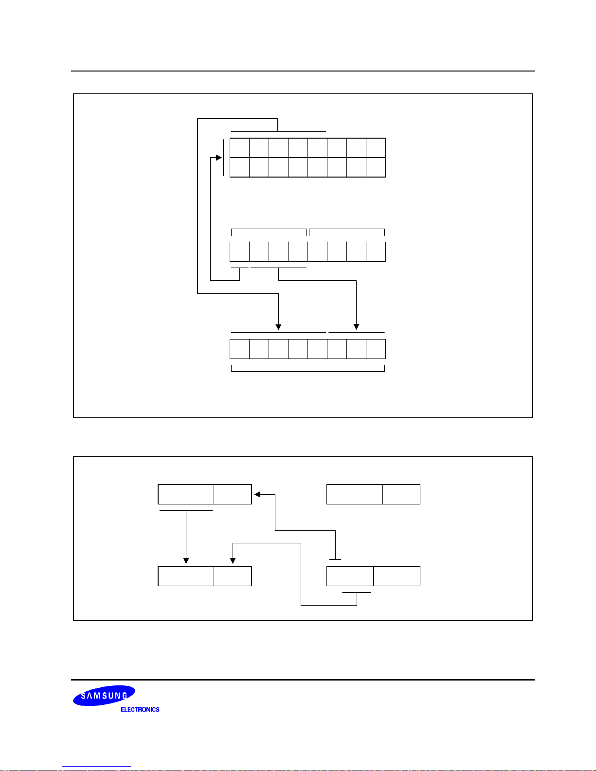
S3C8248/C8245/P8245/C8247/C8249/P8249 ADDRESS SPACES
2-15
Together they create an
8-bit register address
Register pointer
provides five
high-order bits
Address OPCODE
Selects
RP0 or RP1
RP1
RP0
4-bit address
provides three
low-order bits
Figure 2-11. 4-Bit Working Register Addressing
Register
address
(76H)
RP0
0 1 1 1 0 0 0 0
0 1 1 1 0 1 1 0
R6
0 1 1 0 1 1 1 0
Selects RP0
Instruction
'INC R6'
OPCODE
RP1
0 1 1 1 1 0 0 0
Figure 2-12. 4-Bit Working Register Addressing Example
ADDRESS SPACES S3C8248/C8245/P8245/C8247/C8249/P8249
2-16
8-BIT WORKING REGISTER ADDRESSING
You can also use 8-bit working register addressing to access registers in a selected working register area. To
initiate 8-bit working register addressing, the upper four bits of the instruction address must contain the value
"1100B." This 4-bit value (1100B) indicates that the remaining four bits have the same effect as 4-bit working
register addressing.
As shown in Figure 2-13, the lower nibble of the 8-bit address is concatenated in much the same way as for 4-bit
addressing: Bit 3 selects either RP0 or RP1, which then supplies the five high-order bits of the final address; the
three low-order bits of the complete address are provided by the original instruction.
Figure 2-14 shows an example of 8-bit working register addressing. The four high-order bits of the instruction
address (1100B) specify 8-bit working register addressing. Bit 4 ("1") selects RP1 and the five high-order bits in
RP1 (10101B) become the five high-order bits of the register address. The three low-order bits of the register
address (011) are provided by the three low-order bits of the 8-bit instruction address. The five address bits from
RP1 and the three address bits from the instruction are concatenated to form the complete register address,
0ABH (10101011B).
8-bit logical
address
8-bit physical address
Register pointer
provides five
high-order bits
Address
Selects
RP0 or RP1
RP1
RP0
Three low-order bits
These address
bits indicate 8-bit
working register
addressing
1 1 0 0
Figure 2-13. 8-Bit Working Register Addressing
S3C8248/C8245/P8245/C8247/C8249/P8249 ADDRESS SPACES
2-17
8-bit address
form instruction
'LD R11, R2'
RP0
0 1 1 0 0 0 0 0
1 1 0 0 1 0 1 1
Selects RP1
R11
Register
address
(0ABH)
RP1
1 0 1 0 1 0 0 0
1 0 1 0 1 0 1 1
Specifies working
register addressing
Figure 2-14. 8-Bit Working Register Addressing Example
ADDRESS SPACES S3C8248/C8245/P8245/C8247/C8249/P8249
2-18
SYSTEM AND USER STACK
The S3C8-series microcontrollers use the system stack for data storage, subroutine calls and returns. The PUSH
and POP instructions are used to control system stack operations. The S3C8248/C8245/C8247/C8249
architecture supports stack operations in the internal register file.
Stack Operations
Return addresses for procedure calls, interrupts, and data are stored on the stack. The contents of the PC are
saved to stack by a CALL instruction and restored by the RET instruction. When an interrupt occurs, the contents
of the PC and the FLAGS register are pushed to the stack. The IRET instruction then pops these values back to
their original locations. The stack address value is always decreased by one before a push operation and
increased by one after a pop operation. The stack pointer (SP) always points to the stack frame stored on the top
of the stack, as shown in Figure 2-15.
Stack contents
after a call
instruction
Stack contents
after an
interrupt
Top of
stack
Flags
PCH
PCL
PCL
PCH
Top of
stack
Low Address
High Address
Figure 2-15. Stack Operations
User-Defined Stacks
You can freely define stacks in the internal register file as data storage locations. The instructions PUSHUI,
PUSHUD, POPUI, and POPUD support user-defined stack operations.
Stack Pointers (SPL, SPH)
Register locations D8H and D9H contain the 16-bit stack pointer (SP) that is used for system stack operations.
The most significant byte of the SP address, SP15–SP8, is stored in the SPH register (D8H), and the least
significant byte, SP7–SP0, is stored in the SPL register (D9H). After a reset, the SP value is undetermined.
Because only internal memory space is implemented in the S3C8248/C8245/C8247/C8249, the SPL must be
initialized to an 8-bit value in the range 00H–FFH. The SPH register is not needed and can be used as a generalpurpose register, if necessary.
When the SPL register contains the only stack pointer value (that is, when it points to a system stack in the
register file), you can use the SPH register as a general-purpose data register. However, if an overflow or
underflow condition occurs as a result of increasing or decreasing the stack address value in the SPL register
during normal stack operations, the value in the SPL register will overflow (or underflow) to the SPH register,
overwriting any other data that is currently stored there. To avoid overwriting data in the SPH register, you can
initialize the SPL value to "FFH" instead of "00H".

S3C8248/C8245/P8245/C8247/C8249/P8249 ADDRESS SPACES
2-19
++ PROGRAMMING TIP — Standard Stack Operations Using PUSH and POP
The following example shows you how to perform stack operations in the internal register file using PUSH and
POP instructions:
LD SPL,#0FFH ; SPL ← FFH
; (Normally, the SPL is set to 0FFH by the initialization
; routine)
•
•
•
PUSH PP ; Stack address 0FEH ← PP
PUSH RP0 ; Stack address 0FDH ← RP0
PUSH RP1 ; Stack address 0FCH ← RP1
PUSH R3 ; Stack address 0FBH ← R3
•
•
•
POP R3 ; R3 ← Stack address 0FBH
POP RP1 ; RP1 ← Stack address 0FCH
POP RP0 ; RP0 ← Stack address 0FDH
POP PP ; PP ← Stack address 0FEH
 Loading...