


Samsung C3560 Block Diagram 7

Level
8.
Block Diagram
8-1.
Repair
3
8-1
SAMSUNG Proprietary-Contents may change without notice
This Document can not be used without Samsung's authorization
RCV
SPK

Level3Repair
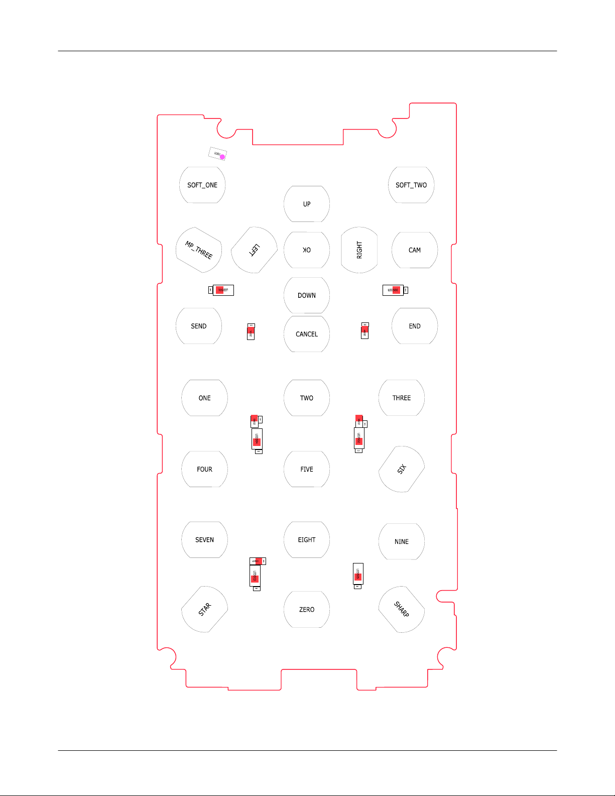
PCB Diagrams
8-2.
8-2-1.
Top
8-2
SAMSUNG Proprietary-Contents may change without notice
This Document can not be used without Samsung's authorization
Level3Repair
8-2-2.
Bottom
8-3
SAMSUNG Proprietary-Contents may change without notice
This Document can not be used without Samsung's authorization

Level3Repair
8-2-3.
SUB Top
8-4
SAMSUNG Proprietary-Contents may change without notice
This Document can not be used without Samsung's authorization

Level3Repair
8-2-4.
SUB Bottom
8-5
SAMSUNG Proprietary-Contents may change without notice
This Document can not be used without Samsung's authorization

Level3Repair
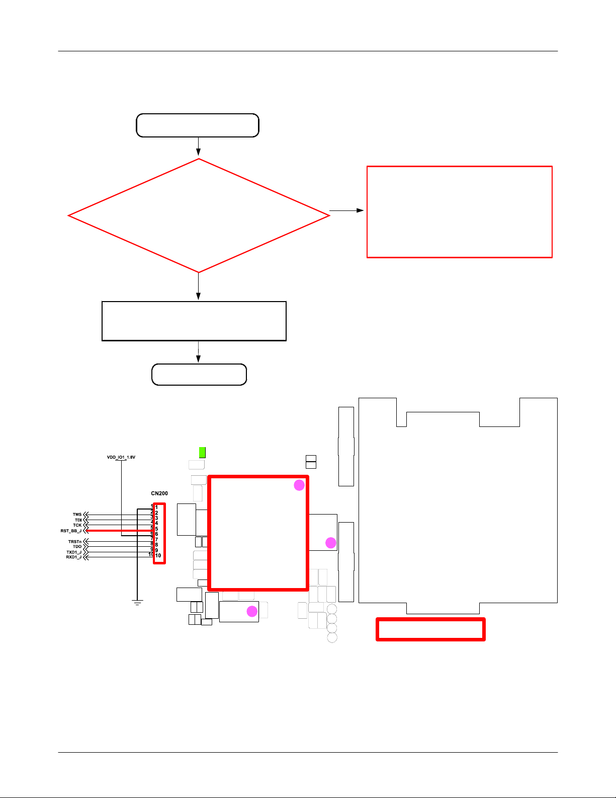
Flow Chart of Troubleshooting
8-3.
8-3-1.
Power On
Power switch on
NG
Check the current
consumption
>= 100
mA?
Yes
Check the battery
voltage
VBAT
>= 3.45?
Yes
Check the voltage
VDD_1.8V(C234)
V?
=1.8
Yes
Check the clock at
OSC201
=26
MHz
?
NO
NO
NO
NO
Download
Change the battery
Check the Main Chip(U202)
Lookover the Chip damage
Resolder OSC201
Yes
END
8-6
SAMSUNG Proprietary-Contents may change without notice
This Document can not be used without Samsung's authorization

U202
ONOFF
SD1SW
SD1_FB
CAS_N
RAS_N
ADV_N
RD_N
RESET_N
TRST_N
WAIT_N
Level3Repair
T16
HSR
A13
XO
B13
XOX
R11
R9
T8
P4
CKE
P5
P2
T4
P1
L15
H17
J8
C
2
2
4
4
0
2
C
C217
C220
DDR_CKE
DDR_CASn
DDR_RASn
NAND_ADVn
NAND_RDn
TRSTn
NAND_WAITn
5
C
2
4
0
EAR_SPK_R
VDD_1.8V
ONKEY
RST_MAX8985
RST_BB_J
RST_BB
R214
2
1
C
L201
C234
VDD_IO1_1.8V
OSC201
4
21
3
4
3
2
C
1
2
2
C
2
0
2
U
O
S
C
2
C
C
2
C400
2
3
3
8
9
8
1
2
C
C235
C236
C222
C226
2
7
2
C228
C
1
1
2
C
C225
C
4
0
3
R
4
0
1
0
1
2
9
1
0
2
2
C
C
C
2
0
0
3
1
1
0
2
2
C
C
8-7
SAMSUNG Proprietary-Contents may change without notice
This Document can not be used without Samsung's authorization
Level3Repair
8-3-2.
Initial
Initial Failure
CN200
ST_BB_J=Pin5
(R
>1.7V?
using the oscilloscope
GND&SHORT PAD.
Yes
Check the16bit data signals.
Yes
END
Yes
)
No
ST_BB_J)must be higher than
R
Resolder U202
1.7V
0
2
R
C
5
2
3
2
C
1
5
C
2
4
0
1
2
2
C
C
C
2
2
3
3
8
9
C235
C236
C222
C226
3
1
0
6
2
0
1
2
2
C
C
C
4
1
2
1
2
R
2
R
2
0
U
2
2
C
2
7
C228
C
0
2
0
S
C
O
2
1
2
0
R210
O
S
C
2
0
1
5
0
1
C
2
0
2
C
C
2
0
3
R
R307
3
0
6
0
2
5
C
S
9
1
2
C
0
1
1
0
2
2
C
C
T
P
_
U
A
R
T
_
T
X
D
T
P
_
U
A
R
R
T
5
_
R
1
X
D
6
TP_BT_RST
T
P
_
1
0
0
SIM500
0
0
2
N
C
8-8
SAMSUNG Proprietary-Contents may change without notice
This Document can not be used without Samsung's authorization

Level3Repair
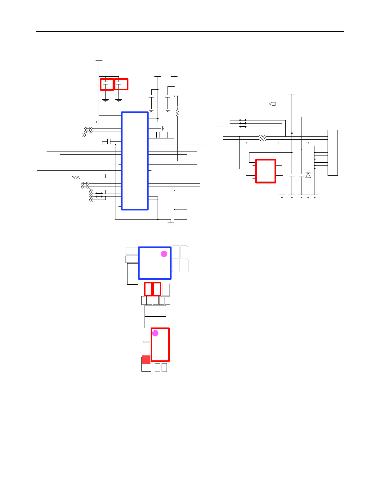
8-3-3.
Charging Part
Abnomal Charging Part
Check the Battery
TA connection
&
Check the voltage
VBUS_5V_IN(C300)
V?
>= 5
Yes
Check the U300
SMD or Damage)
(
?
NG
Yes
NO
NO
NO
Insert the Battery or TA
Check C300, C301, D400
Short to GND or Damage)
(
Change C300, C301, D400
Change the U300
END
Yes
8-9
SAMSUNG Proprietary-Contents may change without notice
This Document can not be used without Samsung's authorization
Level3Repair
VBUS_5V_IN
VBAT
VDD_IO1_1.8V
8985_USB_DM
8985_USB_DP
USB_ID
USB_DM_BB
USB_DP_BB
TXD1_J
UART1_TXD
UART1_RXD
RXD1_J
C305
C301C300
E6
VBUS
D5
BC
D6
COMN1
C6
COMP2
B6
UID
D1
REFBP
C1
AGND
F1
OUT1
E1
OUT2E2RESETB
B1
GPO1
B2
GPO2
E3
VICHG
E5
ADCSL1
F4
ADCSR2
A4
DN1
A5
DP2
C5
UT1
C4
UR2
F6
SL1
F5
SR2
U300
6
0
C308
VBUS_5V_IN
C302
3
0
3
C
VBUS_5V_J
R300
F2
BATT
F3
BATT
A6
DETBAT
B5
C304
VL
A2
VIO
D4
SCL
E4
SDA
A3
IRQB
B4
JIG
C3
ONKEY
C2
RTC2V3
A1
MIC
D2
KEYCOL
D3
KEYROW
B3
ONKEYN
1
NC
2
NC
C
3
U
3
0
0
2
0
3
C
0
0
3
C
R
3
3
0
0
1
3
R
5
1
C
C
3
1
0
1
3
5
R
3
9
0
0
5
3
C
C
1
3
0
0
3
4
C
R
R
3
3
4
0
0
0
2
0
3
R
4
C
MICRO USB - PBA TEST JIG PIN
R414
R415
1
VBUS
2
VBAT
3
DATA-
4
DATA+
5
ID
6
FM_RADIO
D400
GND
GND
VBAT
IFC400
1
1
2
2
3
3
4
4
5
5
6
S1
7
S2
8
NC
9
NC
10
NC
D401
11
NC
12
NC
13
NC
8
7
C415
C414
C414
4
1
4
R
D
4
0
0
5
1
4
R
1
0
4
C
0
4
D
1
1
4
2
C
8-10
SAMSUNG Proprietary-Contents may change without notice
This Document can not be used without Samsung's authorization

Level3Repair
8-3-4.
LCD Working
Power Switch On
LCD FPCB
connector is corre
ctly connectied?
Main FPCB
connector is corre
ctly connectied?
NO
correctly connect
Yes
correctly connect
NO
Yes
Check
C105
C106
=2.9V
=1.8V
Yes
Screen error
Break out line
-
Yes
LCD Replace
NO
Yes
C105, C106
Resolder
F500, F502
Resolder
8-11
SAMSUNG Proprietary-Contents may change without notice
This Document can not be used without Samsung's authorization