

Page 1
13 Circuit Descriptions
13-1
13 Circuit Descriptions
13-1 Overall Block Structure
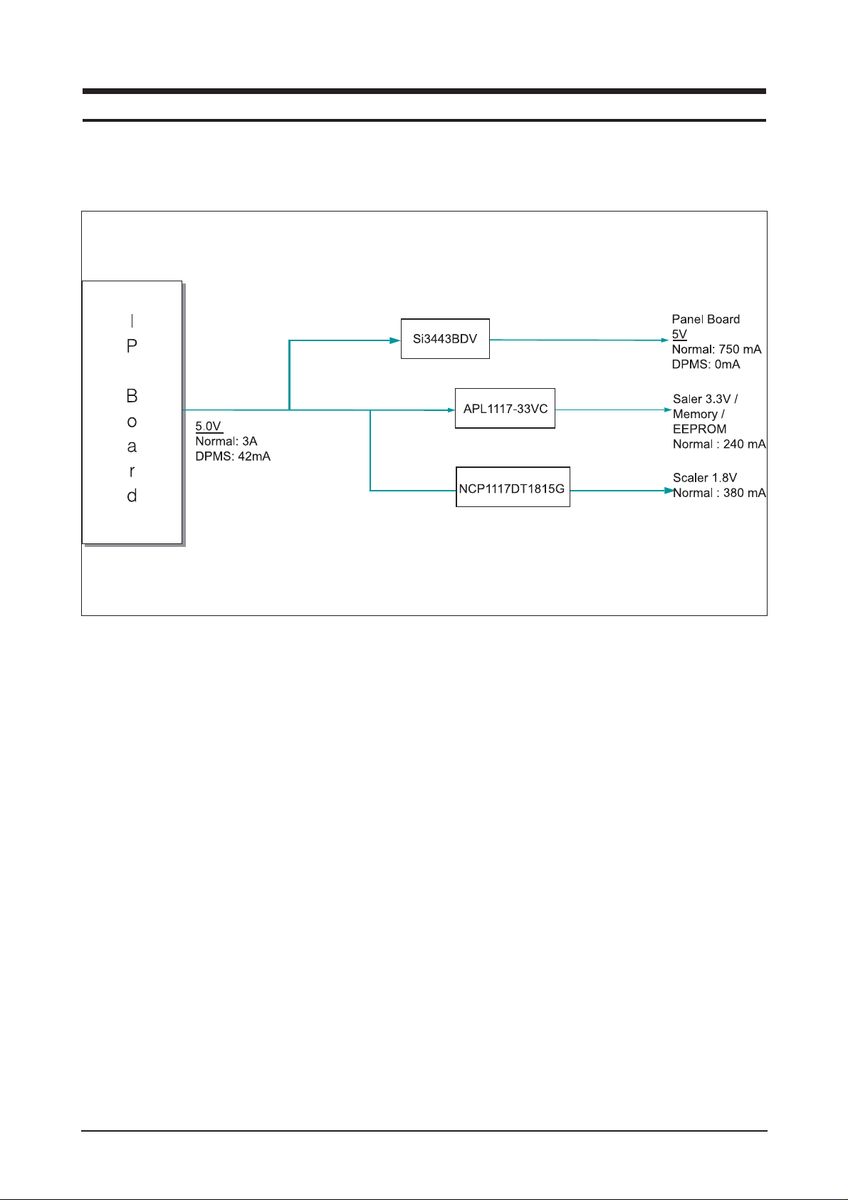
13-1-1 Power Tree
1. When the AD board is in DPMS state:
1.1 The IP has been designed so that it operates with a power consumption of less than 0.6W of.
1.2 The Scaler consumes power up to 37mA
1.3 The power to the panel is switched off
2. When the AD board is operating normally:
2.1 The maximum power consumption of the panel lamps is described below (It may vary depending on
the panel manufacturer)
4 x (7.5mA x 720mVrms)=4 x 5.4=21.6W
2.2 The power consumption of the Panel Control board is as follows: 5V x 720mA=3.6W
2.3 The power consumption of the Scaler is as follows: 3.3V x 245mA + 1.8V x 300mA = 1.35W
Page 2
13 Circuit Descriptions
13-2
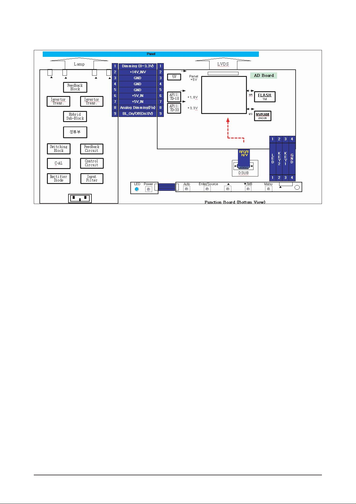
13-1-2 Main Board Parts
1. Inverter: A conversion device that converts DC
rated voltage/current to high ones necessary
for the panel lamp.
2. DC/DC(Regulator): General term for DC to DC
converting devices.
The IP board receives 5V and outputs 1.8 or
3.3V that is supplied to the scaler (SE567MRHLF).
3. Power MosFET: The IP board receives 5V and
outputs a lower voltage in DPMS mode and
supplies the whole 5V for the panel operating
board in normal conditions. In that case, the
switching of Power MosFET is controlled by
Micom.
4. Scaler: Receives the digital TMDS and analog
R,G,B signals and convert them to proper resolutions using up- or down- scaling that are
transferred to the panel in the LDVS formats.
5. Crystal(Oscillator): Use one 14.318MHz oscillator externally to supply power to both MCU and
Scaler at the same time.
6. SCALER & EEPROM: I2C is a two-way serial
bus of two lines that supports communications
across the integrated circuits as well as
between FLASH and EEPROM.
In particular, FLASH and Scaler (SE567MRHLF) use the SDR direct bus for mutual communications, which is an effective, speedy system
because it allows 4 additional address/data
lines compared to the old serial systems.
7. Function Key: A certain keystroke generates a
certain electrical potential, which is transferred
into ADC input port of the Scaler and then converted to a digital value by the A/D converter of
the chip. The digital value (data) is a clue to
which key is entered. In practical, the voltage
levels are set as below.
Page 3
13 Circuit Descriptions
13-3
13-1-3 IP BOARD BLOCK(POWER) Parts
13-1-4 IP BOARD BLOCK( INVERTER ) Parts
Page 4

13 Circuit Descriptions
13-4
13-1-5 IP BOARD(inverter) PROTECTION Parts
PROTECTION Parts
- PROTECTION Parts are divided two parts. When lamp voltage rose as absurd and lamp feedback electric
current would not be sensed. So all of the two halt IP-Board's function that prevent action the enemy more
than IP-Board's continous abnormality action.
- When Trans output voltage rose as absurd, become OVP and halts IP-board's function because the
divided voltage is inputted by IC(U201) 2 PIN.
- When lamp current is sensed, become OLP and halts IC because the IC(U201) 2 PIN is became
under 2.5V
Page 5

13 Circuit Descriptions
13-5
13-2 Trouble Shooting
13-2-1 IP BOARD(Power)
Check Fuse (F101)
IC101 Vst-Pin
(Norma:High)
Change FUSE
Check the short of AC part or
IC101 D-pin
Check the 13V output part
open
No
No
Yes
IC101 Vcc-Pin
(Normal:9~16V)
Yes
IC101 D-Pin
(Normal:Switching)
Yes
Power On
No
Check the Switching part
No
Check the Vcc part
No
Check the protection system
Check others Harness, Inlet
Output 13V
(Normal:12~14V)
Yes
No
Check the feedback system
No
Inlet/Output
Harness
Yes
Yes
Check the Pin or wire
connection
No
Check the IC
No
Page 6

13 Circuit Descriptions
13-6
13-2-1 IP BOARD(Inverter)
Check the 13V line
16Pin
(Normal:5Vtyp.)
Yes
Control IC is
(Pin 12, 13 : chopping wave
Pin 8, 9 : square wave)
Yes
Power On
Check the Control IC & IC
Driver
No
Check the Input Circuit
No
Check the Protection Circuit
Check others Harness, Inlet
Inverter Trans
(Pin8,9 : square wave)
Yes
No
Check the Dimming Circuit
No
Check the Half-bridge part
No
Output Current
(Normal Output)
Yes
Yes
Check the Feedback Circuit
No
Check the Adapter system
No
Page 7

13 Circuit Descriptions
13-7
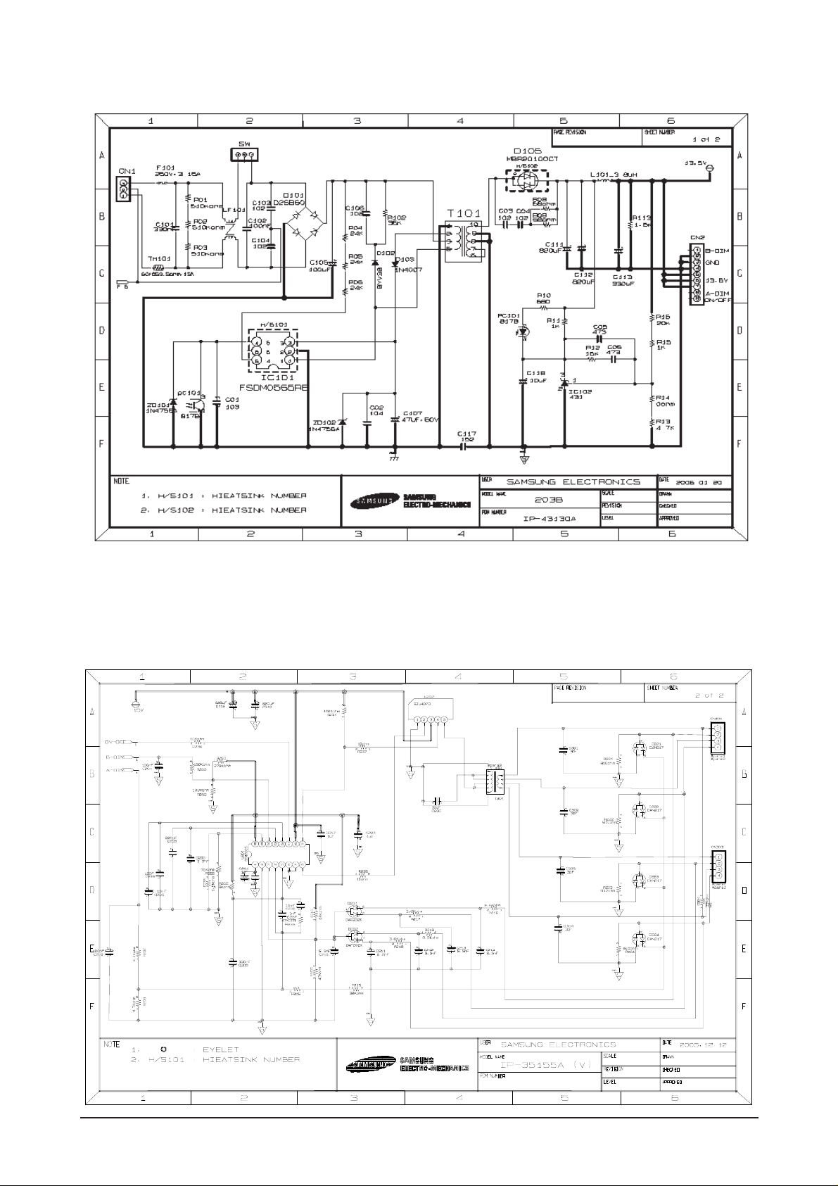
13-3 IP BOARD(Power) Schematic Diagrams
Page 8

13 Circuit Descriptions
13-8
13-4 IP BOARD(Inverter) Schematic Diagrams
 Loading...