

Page 1
Level
8.
Block Diagram
8-1.
ONKEY
ONKEY
ONKEY
ONKEY
CHARGER
CHARGER
CHARGER
CHARGER
LCD
LCD
LCD
LCD
3.2”WQVGA
3.2”WQVGA
3.2”WQVGA
3.2”WQVGA
WTSP
WTSP
WTSP
WTSP
HapticMotor
HapticMotor
Repair
3
Master Memory
Master Memory
Master Memory
Master Memory
4G x 1G
4G x 1G
4G x 1G
4G x 1G
NAND / SDRAM
NAND / SDRAM
NAND / SDRAM
NAND / SDRAM
Keypad
Keypad
Keypad
Keypad
SIM
SIM
SIM
SIM
T-Flash
T-Flash
T-Flash
T-Flash
Master PMU
Master PMU
Master PMU
Master PMU
(PCF50623)
(PCF50617)
(PCF50623)
(PCF50617)
Mot/Touch IC
Mot/Touch IC
Mot/Touch IC
Mot/Touch IC
(ISA2000)
(ISA2000)
Acc Sensor
Acc Sensor
KR3DF
KR3DM
Camera
Camera
5M AF
5M AF
CIF CAM
CIF CAM
SWITCH
SWITCH
SWITCH
SWITCH
common I2C
common I2C
common I2C
common I2C
common I2C
common I2C
Master RF
Master RF
Master RF
Master RF
(HSDPA)
(HSDPA)
(HSDPA)
(HSDPA)
AERO4229
AERO4229
AERO4229
AERO4229
Master B/B
Master B/B
Master B/B
Master B/B
(PNX6709)
(PNX6709)
(PNX6709)
(PNX6709)
UART2
UART2
UART2
UART2
GPIO
GPIO
GPIO
GPIO
EXTINT
EXTINT
EXTINT
EXTINT
GPIO
GPIO
GPIO
GPIO
EXTINT
EXTINT
EXTINT
EXTINT
EAR
EAR
Ana In
RCV
RCV
SPK
EAR
USB
MIC1 MIC2 UART1
MIC1 MIC2 UART1
USB
SPI2
SPI2
SPI2
SPI2
SPI1
SPI1
SPI1
SPI1
Data Communication
Data Communication
Interrupt for data
Interrupt for data
Interrupt for debugging
Interrupt for debugging
FM
FM
TEA5991
TEA5991
WIFI(SWL-10)
WIFI(SWL-10)
WIFI(SWL-10)
WIFI(SWL-10)
BT(BC6)
BT(BC6)
BT(BC6)
BT(BC6)
PCM
PCM
PCM
PCM
SWITCH
SWITCH
SWITCH
SWITCH
Audio
Audio
Amp
Amp
SWITC
SWITCH
SWITCH
Slave RF
Slave RF
Slave RF
Slave RF
QS520
QS520
QS520
QS520
Slave B/B
Slave B/B
Slave B/B
Slave B/B
(PNX6608)
(PNX6608)
(PNX6608)
(PNX6608)
UART2
UART2
UART2
UART2
EXTINT
EXTINT
EXTINT
EXTINT
GPIO
GPIO
GPIO
GPIO
EXTINT
EXTINT
EXTINT
EXTINT
GPIO
GPIO
GPIO
GPIO
EAR
HFR_S
USB
USB
UART1 MIC2 MIC1
UART1 MIC2 MIC1
SWITCH
SWITCH
SWITCH
SWITCH
Slave Memory
Slave Memory
Slave Memory
Slave Memory
128Mx64M
128Mx64M
128Mx64M
128Mx64M
NOR/
NOR/
NOR/
NOR/
UtRAM
UtRAM
UtRAM
UtRAM
SIM
SIM
SIM
SIM
SLAVEON (mater)
SLAVEON (mater)
SLAVEON (mater)
SLAVEON (mater)
Master
Master
Slave
Slave
SWITCH
SWITCH
SWITCH
SWITCH
SWITCH
SWITCH
USB UART EARSPK
USB UART EARSPK
EARMIC
EARMIC
Micro usbswitch
Micro usbswitch
Micro usb con
Micro usb con
8-1
SAMSUNG Proprietary-Contents may change without notice
This Document can not be used without Samsung's authorization
Common
Common
Page 2
Level3Repair
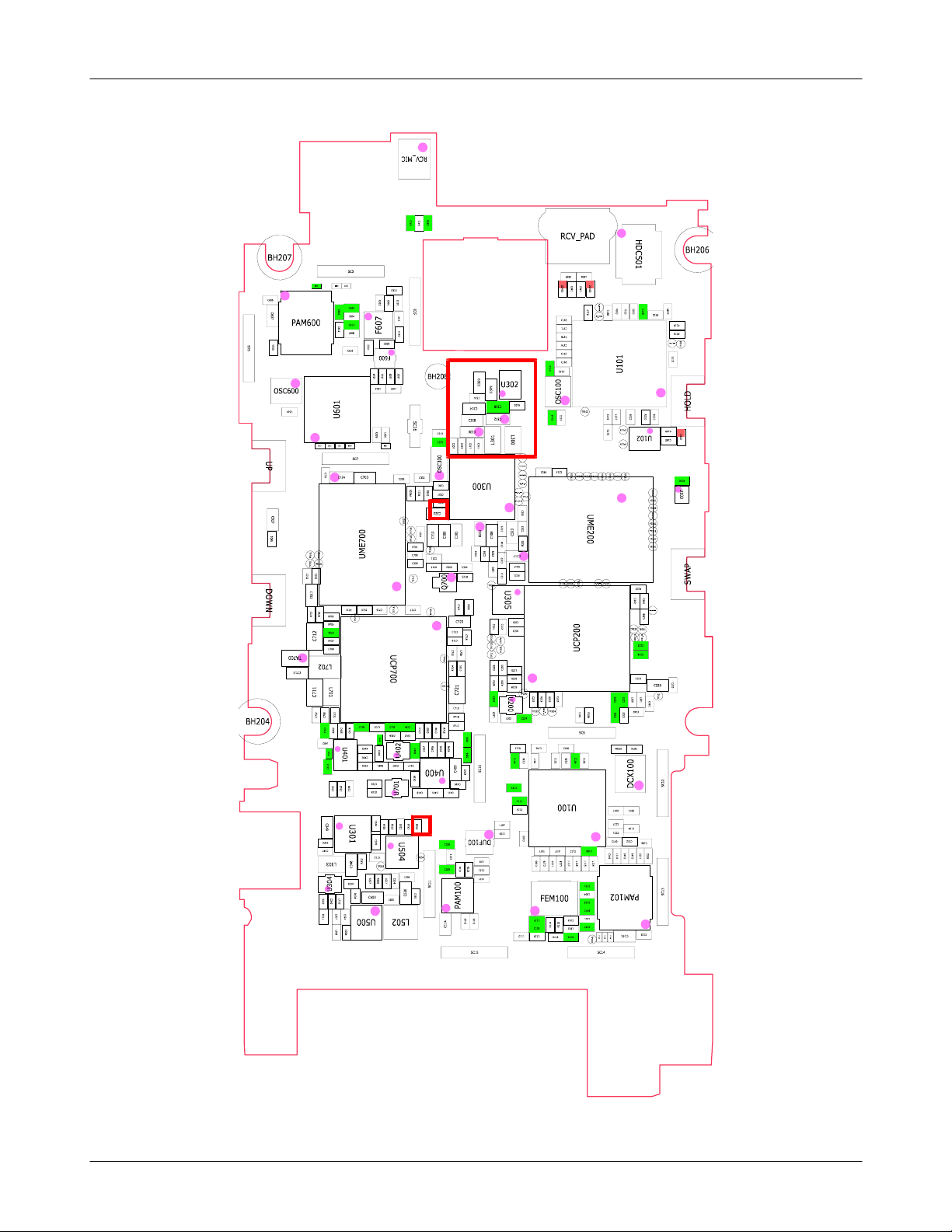
PCB Diagrams
8-2.
8-2-1.
Top
8-2
SAMSUNG Proprietary-Contents may change without notice
This Document can not be used without Samsung's authorization
Page 3
Level3Repair
8-2-1.
Bottom
8-3
SAMSUNG Proprietary-Contents may change without notice
Page 4
Level3Repair
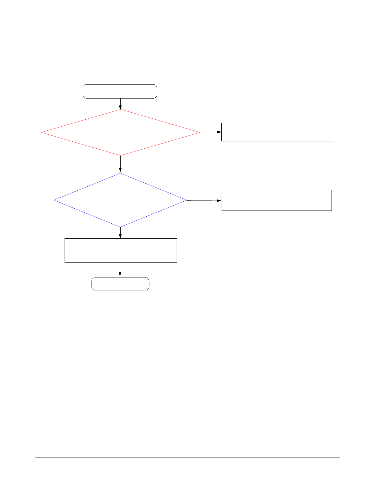
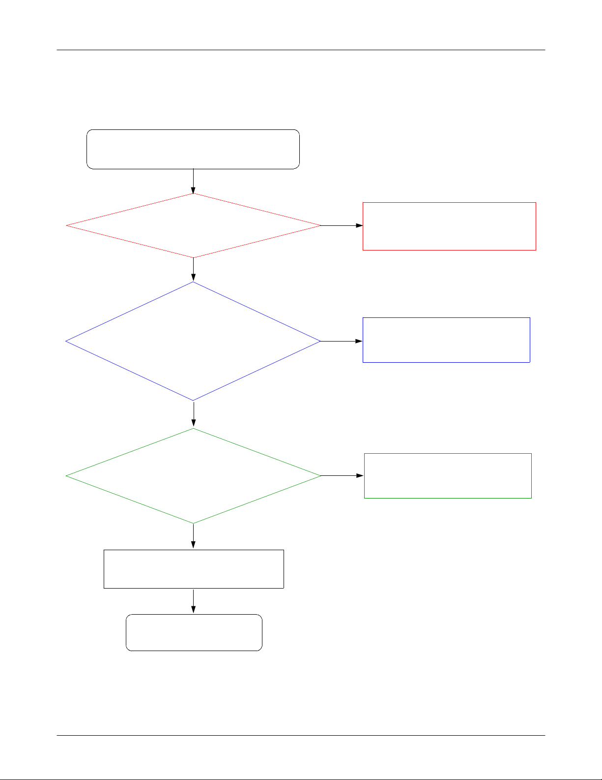
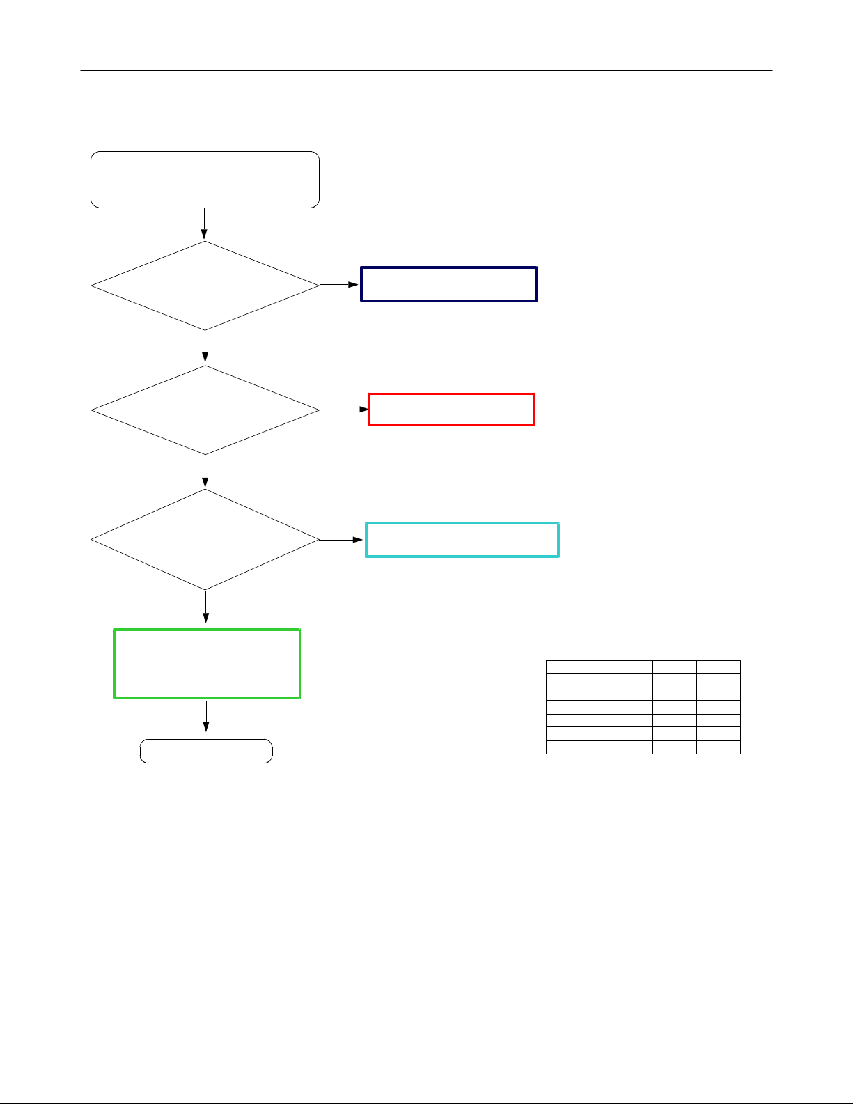
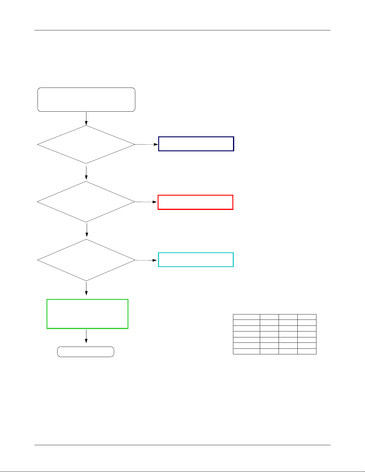
Flow Chart of Troubleshooting
8-3.
presetting methods for checking TP
※
GND&TP(exp. Vbatt=C108, C109, C212,C308)using Oscilloscope
-
look over the coming out signal.
-
Oscilloscope
←
8-4
SAMSUNG Proprietary-Contents may change without notice
This Document can not be used without Samsung's authorization
Page 5
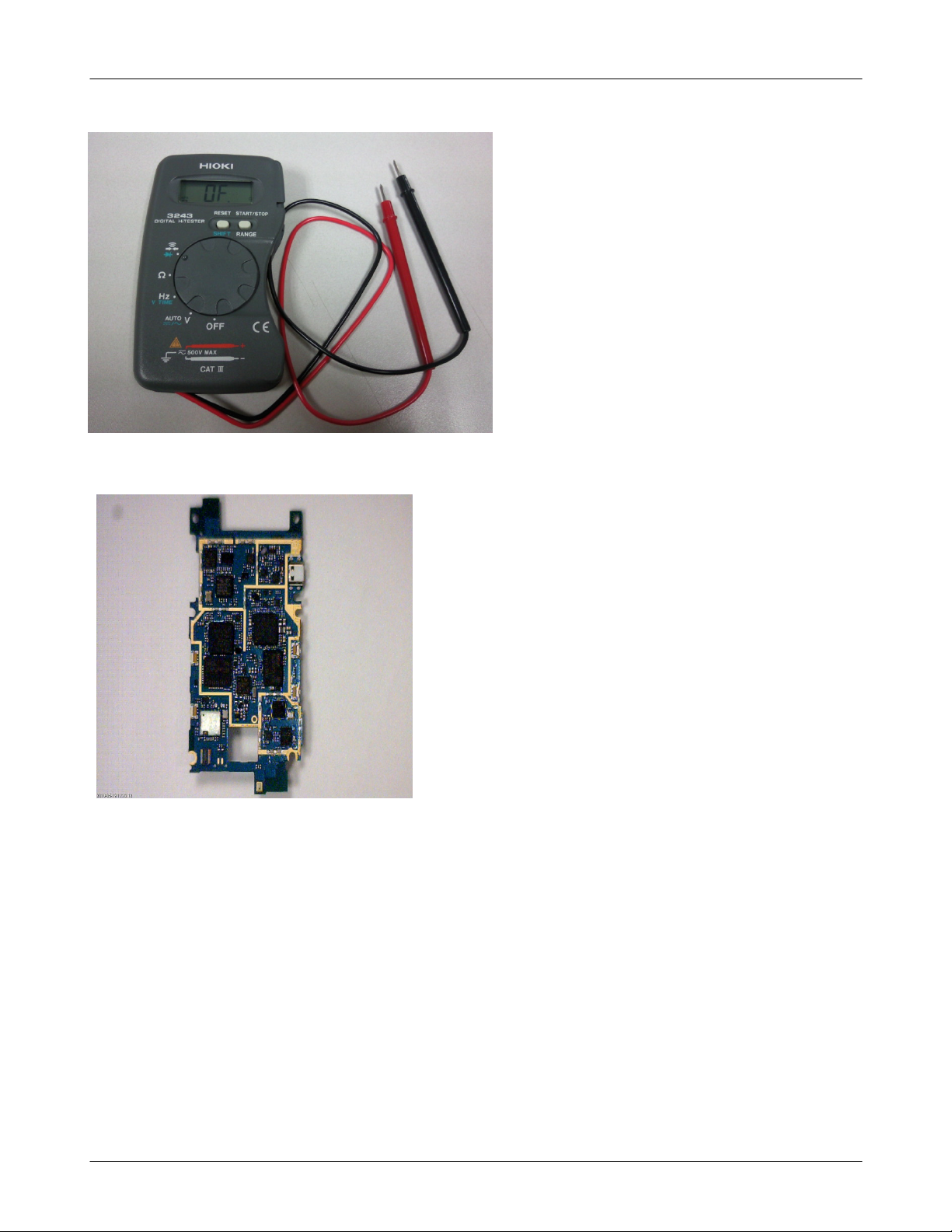
Multi-meter
←
Level3Repair
EX) to look up the TP, shunt Cap.
-
SAMSUNG Proprietary-Contents may change without notice
Checking the TP(test point) using Multi-meter
←
if checking the GND, you can listen"beep"
-
if checking the Signal, you can't listen it.
8-5
Page 6
Level3Repair
8-3-1.
Power On
Power On'does not work
'
Check the Battery Voltage
is more than
C300, C311,C501)
(
VDD_IO_LOW_1.8V
C213,
(
Check the Clock at
OSC300(CLK32K)
C332, C333)
(
Yes
Yes
=1.8V ?
214)
Yes
3.3V
=32
KHZ
No
No
No
Change the Battery
Because of batt. power low)
(
Check the Main Chip related to
VDD_IO_LOW_1.8V
to look over the Chip damage)
(
Check the Main Chip
to lookover the Chip damage)
(
C332, C333/look over the waverform
(TP:
using the oscilloscope)
Yes
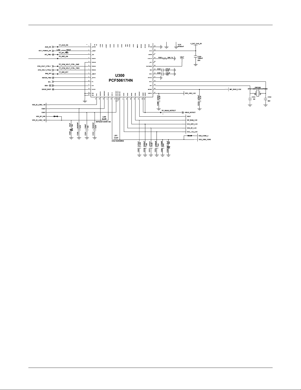
VDD_CORE_2
L301, C328, C330)
(
Yes
END
=1.2
V?
No
Resolder L301, C328, C330
to confirm coming out power V_core)
(
8-6
SAMSUNG Proprietary-Contents may change without notice
This Document can not be used without Samsung's authorization
Page 7
Level3Repair
8-7
SAMSUNG Proprietary-Contents may change without notice
Page 8
Level3Repair
8-8
SAMSUNG Proprietary-Contents may change without notice
This Document can not be used without Samsung's authorization
Page 9
Level3Repair
8-3-2.
Initial
Initial Failure
Yes
UCP200 pin E7(RSTON)
="H(>2.4V)"?
C227)
(
Yes
Slaveon signal is changed
-> L→H
in boot sequence
R723&R719
(
)
No
H
No
Replace UCP200, must be"H"
Replace Q700 and check once again
Yes
Check the16bit data signal
memory CE(TP214,TP215)
&
Yes
END
8-9
SAMSUNG Proprietary-Contents may change without notice
Page 10
Level3Repair
8-10
SAMSUNG Proprietary-Contents may change without notice
This Document can not be used without Samsung's authorization
Page 11
Level3Repair
8-11
SAMSUNG Proprietary-Contents may change without notice
Page 12
Level3Repair
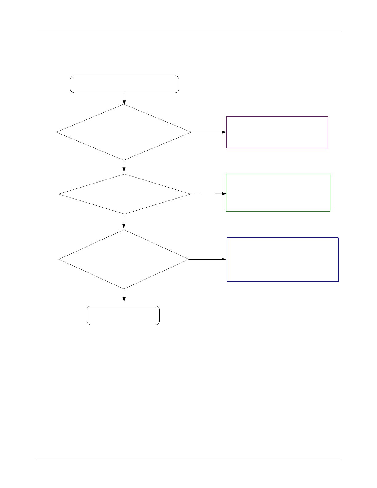
8-3-3.
Charging Part
Check VBUS voltage
(
Abnormal charging part
Yes
TP:C438,1pin of IFC400)
U404 pin
15 (
>4.9V
TP:C435)
(
>4.9V
Yes
OUT)
Yes
No
(
No
be possible that it's not soldering well)
(
Resolder IFC400, C438
be possible that it's not soldering well)
Resolder U404
U300 pin
>4.9V
TP:C325)
(
38(
END
VCHG)
Yes
No
Resolder C325, C435
and
Replace U300 usingaHeatgun
8-12
SAMSUNG Proprietary-Contents may change without notice
This Document can not be used without Samsung's authorization
Page 13
Level3Repair
8-13
SAMSUNG Proprietary-Contents may change without notice
Page 14
Level3Repair
8-14
SAMSUNG Proprietary-Contents may change without notice
This Document can not be used without Samsung's authorization
Page 15
Level3Repair
8-3-4.
Sim Part
Phone can't access SIM Card
Yes
SIM
or R307 and R308
Check SIMClk Signal on
pin3 of SIM
method:wiring pin3and
(
checking its waveform using an
SIM301 pin
300,
"H=3.0V" ?
Yes
After Power ON,
SIM301 inafew
300,
second
oscilloscope)
1
No
No
Resolder R300, U305
insert SIM card&access it,
then must be"H=3.0V"
Resolder or Replace SIM
connector.(Because of not soldering well)
300,
SIM301
Yes
After SIM card insert,
SIM
method:wiring pin3and check
(
SIM301 pin2(SIM_RST)
300,
= "H=3.0V"?
its waveform using an
oscilloscope) oscilloscope)
Yes
Check the SIM Card
look over if it get damaged.)
(
Yes
END
No
Confirm an another PBA
8-15
SAMSUNG Proprietary-Contents may change without notice
Page 16
Level3Repair
8-16
SAMSUNG Proprietary-Contents may change without notice
This Document can not be used without Samsung's authorization
Page 17
Level3Repair
8-17
SAMSUNG Proprietary-Contents may change without notice
Page 18

Level3Repair
8-3-5.
Microphone Part
Microphone does not work
U300 pin U28
Mic_bias="2.15V"?
TP:C313)
(
Check the MIC Connection
look over schematics about
(
schemetics.)
Yes
Yes
Yes
No
No
Replace U300 usingaHeatgun
Because of not soldering well
(
Resolder C535, ZD502, U402, C417, C451
C448, C416, R410, U401, R402, L401, L402
not work if those is not connected.)
(
)
Check the MIC sample.
it be possible the problem
(
things)
Yes
END
No
Replace an another MIC
because of being possible the problem)
(
8-18
SAMSUNG Proprietary-Contents may change without notice
This Document can not be used without Samsung's authorization
Page 19

Level3Repair
8-19
SAMSUNG Proprietary-Contents may change without notice
Page 20

Level3Repair
8-20
SAMSUNG Proprietary-Contents may change without notice
This Document can not be used without Samsung's authorization
Page 21

Level3Repair
8-3-6.
Speaker Part
produces signal(voltage)
(
checking an waveform using
Speaker does not work
Yes
Check L404 and L405
Wiring the SPK N/P and
oscilloscope)
Yes
Is Speaker working?
Listening through the
(
speaker)
Yes
No
Resolder L404 AND L405, ZD402, ZD403
be possible because of soldering not well)
(
No
Change Speaker ASS'Y
be possible of SPK Problems
(
or not inserting it right.)
Does not work spkaer
mode and receiver mode?
(*#0*#
select the Call ringtone)
check receiver
→
and speaker)
Yes
END
No
Resolder or Replace UCP200, U400
be possible of soldering not well or being
(
UCP
bad sample)
a
8-21
SAMSUNG Proprietary-Contents may change without notice
Page 22

Level3Repair
8-22
SAMSUNG Proprietary-Contents may change without notice
This Document can not be used without Samsung's authorization
Page 23

Level3Repair
8-3-7.
Key Data Input
Check Initial Operation
When you pushed all of the
Key, does the key have
Yes
tension?
Yes
No
(#1 :
#3
whether be sunken
look over the Dome location
#2 :
whether be out of line
look over TACT switch was broken
or be short)
Change Domesheet
look over the Dome situation
All of the key doesn't work
except POWER ON KEY
Yes
END
No
?
because of be possible for FPCB to get damaged)
Replace the FPCB and diode
over the insturctions again
(
8-23
SAMSUNG Proprietary-Contents may change without notice
Page 24

Level3Repair
8-24
SAMSUNG Proprietary-Contents may change without notice
This Document can not be used without Samsung's authorization
Page 25

Level3Repair
8-3-8.
Bluetooth
8-25
SAMSUNG Proprietary-Contents may change without notice
Page 26

Level3Repair
Bluetooth does not work
Yes
U101 pin
4dBm
Check U101 pin
≥1.8V
pin
44
pin4 ≥ 3.3V
Check U101 pin6
MHz
26
15
≥
Yes
13,24,42,51
≥2.6V
Yes
?
Yes
No
No
No
Resolder or Replace U101
Resolder U101 and U300
Resolder or replace C122, U100
Check
& Resolder U102
Yes
END
8-26
SAMSUNG Proprietary-Contents may change without notice
This Document can not be used without Samsung's authorization
Page 27

Level3Repair
8-27
SAMSUNG Proprietary-Contents may change without notice
Page 28
Level3Repair
8-28
SAMSUNG Proprietary-Contents may change without notice
This Document can not be used without Samsung's authorization
Page 29

Level3Repair
8-3-9.
WiFi
WiFi does not work
U101 pin
10dBm
Check U101 pin
≥1.8V
pin
44
pin 32,33 ≥ 3.3V
pin 40 ≥ 1.2V
Yes
15
≥
Yes
13,24,42,51
≥2.6V
Yes
No
No
Resolder or Replace U101
Resolder U101 and U300
Check OSC100 pin1 or
MHz
40
?
Yes
Check
& Resolder U103
Yes
END
3
No
Resolder or Replace OSC100
8-29
SAMSUNG Proprietary-Contents may change without notice
Page 30
Level3Repair
8-30
SAMSUNG Proprietary-Contents may change without notice
This Document can not be used without Samsung's authorization
Page 31

Level3Repair
8-31
SAMSUNG Proprietary-Contents may change without notice
Page 32

Level3Repair
presetting
※
Rx setting)
(
Tx setting)
(
8960
Active Cell
1.
select GSM or GPRS
:
Connetion Type
2.
select Auto
:
BCH Parameter
3.
select measuring band(DCS or EGSM)
:
Cell power
4.
dBm
:-60
After setting
※
8960 (
EGSM/DCS
)
After setting, prepare the call setup Display
1.
Using an Originate Call, makeacall.
2.
Confirm the display"connected"
3.
start the measuring
4.
8-32
SAMSUNG Proprietary-Contents may change without notice
This Document can not be used without Samsung's authorization
Page 33

Level3Repair
※
8960 &
spectrum analyzer
down&up at picture)
(
spectrum analyzer:testing method=the way using an Osciliscope
-
-8960:
connect using RF Cable between
8960 &
RF Connector in board.
Master RF Connector
Slave RF Connector
8-33
SAMSUNG Proprietary-Contents may change without notice
Page 34

Level3Repair
8-3-10.
Master GSM900 Receiver
RX ON
Cell Power
Check C159
Soldering
Check FEM100
Soldering
Check
L116,L117,C172
Soldering
:-60
Yes
Yes
Yes
dBm
No
No
No
Resolder C159
Resolder FEM100
Resolder L116,L117,C172
Yes
Check&Resolder
U100
Yes
END
FEM CONTROL
TX_GSM850/900
TX_DCS/PCS
RX_GSM850/900
RX_DCS/PCS
B1_TRX
B8_TRX
RFSM1
1
1
0
0
1
1
RFSM3RFSM2
1
0
1
0
1
0
1
0
1
1
0
1
8-34
SAMSUNG Proprietary-Contents may change without notice
This Document can not be used without Samsung's authorization
Page 35
Level3Repair
8-3-11.
Master DCS Receiver
RX ON
Cell Power
Check C159
Soldering
Check FEM100
Soldering
Check
L118,
Soldering
L
119,
:-60
Yes
Yes
Yes
L120
dBm
No
No
No
Resolder C159
Resolder FEM100
Resolder L118,L119,L120
Yes
Check&Resolder
U100
Yes
END
FEM CONTROL
TX_GSM850/900
TX_DCS/PCS
RX_GSM850/900
RX_DCS/PCS
B1_TRX
B8_TRX
RFSM1
1
1
0
0
1
1
RFSM3RFSM2
1
0
1
0
1
0
1
0
1
1
0
1
8-35
SAMSUNG Proprietary-Contents may change without notice
Page 36

Level3Repair
8-3-12.
Master
3G
Receiver
RX ON
Cell Power
:-60
dBm
Yes
FEM100 sensitivity
-105
Yes
Check&Resolder
C131,L101,L123,L103,
DUF100,C105,L109,L107
≥
No
Check&Resolder C159
END
Yes
FEM CONTROL
TX_GSM850/900
TX_DCS/PCS
RX_GSM850/900
RX_DCS/PCS
B1_TRX
B8_TRX
RFSM1
1
1
0
0
1
1
RFSM3RFSM2
1
0
1
0
1
0
1
0
1
1
0
1
8-36
SAMSUNG Proprietary-Contents may change without notice
This Document can not be used without Samsung's authorization
Page 37

RFSM1
RFSM2
RFSM3
Level3Repair
RFS100
G
C
G
A
3
4
1
2
C136
C137
9
PCN|PCS_TX
11
GSM850|EGSM_TX
4
CTRL1
5
CTRL2
6
CTRL3
L113
2
FEM100
1
C159
RF2G_VDD_RF2
L102
C163
7
T
D
N
D
A
V
16
PCN_RX
17
PCN_RX
18
PCS_RX
19
PCS_RX
12
GSM850_RX
13
GSM850_RX
14
EGSM_RX
15
EGSM_RX
20
WCDMA
22
WCDMA
D
D
D
D
D
D
D
N
N
N
N
N
N
N
G
G
G
G
G
G
G
1
0
8
4
3
3
2
1
2
2
L118
L120
C179
C180
L115
L116
L119
L121
L114
C169
C172
L117
4
M
S
F
R
B8_TRX
B1_TRX
L112
DPCS_TX
GSM_TX
R114
R115
R116
8-37
SAMSUNG Proprietary-Contents may change without notice
Page 38

Level3Repair
8-38
SAMSUNG Proprietary-Contents may change without notice
This Document can not be used without Samsung's authorization
Page 39

Level3Repair
8-3-13.
Master GSM Transmitter
TX ON(5Level)
Yes
FEM100 Pin
PAM102 pin
30
30
dBm
No
dBm
16
2
≥
≥
yes
Yes
Resolder C159
Resolder L104, FEM100
No
PAM102 pin
≥
-4
dBm
6
No
Check&Resolder
U100
Yes
END
Yes
Resolder PAM102,C149
FEM CONTROL
TX_GSM850/900
TX_DCS/PCS
RX_GSM850/900
RX_DCS/PCS
B1_TRX
B8_TRX
RFSM1
1
1
0
0
1
1
RFSM3RFSM2
1
0
1
0
1
0
1
0
1
1
0
1
8-39
SAMSUNG Proprietary-Contents may change without notice
Page 40
Level3Repair
8-3-14.
Master DCS Transmitter
TX ON(0Level)
Yes
FEM100 Pin
PAM102 pin
28
28
dBm
No
dBm
16
19≥
≥
yes
Yes
Resolder C159
Resolder L111, FEM100
No
PAM100 pin
≥
-4
dBm
4
No
Check&Resolder
U100
Yes
END
Yes
Resolder PAM102,C110
FEM CONTROL
TX_GSM850/900
TX_DCS/PCS
RX_GSM850/900
RX_DCS/PCS
B1_TRX
B8_TRX
RFSM1
1
1
0
0
1
1
RFSM3RFSM2
1
0
1
0
1
0
1
0
1
1
0
1
8-40
SAMSUNG Proprietary-Contents may change without notice
This Document can not be used without Samsung's authorization
Page 41

Level3Repair
8-3-15.
Master
Transmitter
3G
TX ON(Target Power24dBm
Yes
FEM100 Pin
20
dBm
2
≥
No
PAM100 pin
20
dBm
9
≥
)
yes
Yes
Resolder C159
Resolder DUF100,C131,C103
No
Check&Resolder
PAM100, C130, U100
Yes
END
FEM CONTROL
TX_GSM850/900
TX_DCS/PCS
RX_GSM850/900
RX_DCS/PCS
B1_TRX
B8_TRX
RFSM1
1
1
0
0
1
1
RFSM3RFSM2
1
0
1
0
1
0
1
0
1
1
0
1
8-41
SAMSUNG Proprietary-Contents may change without notice
Page 42

Level3Repair
DCS_PA
GSM_PA
PON_PA
BAND_SEL
VRAMP
DPCS_TX
GSM_TX
R114
RFSM1
R115
RFSM2
R116
RFSM3
C155
C145
RFS100
G
G
3
4
L112
L110
C
A
1
2
C137
9
PCN|PCS_TX
11
GSM850|EGSM_TX
4
CTRL1
5
CTRL2
6
CTRL3
C153
C159
L113
2
FEM100
1
VBAT
C129
C146
C154
C141
26
4
DCS|PCS_IN
6
GSM_IN GSM_OUT
23
TX_EN
22
BS
24
VRAMP
25
VLOGIC
TP100
G
G
G
G
G
G
5
3
1
9
7
8
2
VBATT
PAM102
G
G
G
G
G
G
G
G
G
G
2
0
1
3
1
1
1
1
G
4
5
7
8
0
1
1
1
1
1
2
2
7
2
G
G
8
2
DCS|PCS_OUT
G
G
G
9
1
0
2
3
3
19
16
38
G
37
G
36
G
35
G
G
G
G
2
3
4
3
3
3
L111
C147
L104
C152
DPCS_TX
C148
GSM_TX
C151
VBAT
C136
RF2G_VDD_RF2
L102
PCN_RX
PCN_RX
PCS_RX
PCS_RX
GSM850_RX
GSM850_RX
EGSM_RX
EGSM_RX
WCDMA
WCDMA
D
N
G
4
2
C163
16
17
18
19
12
13
14
15
20
22
L118
L120
C179
C180
L115
L116
L117
B8_TRX
B1_TRX
L119
L121
L114
C169
B1_PA_IN
3G_BYPASS
3G_RAMP
3G_PA_EN1
C172
C118
7
T
D
N
D
A
V
D
D
D
D
D
D
N
N
N
N
N
N
G
G
G
G
G
G
3
3
0
8
1
2
1
2
4
M
S
F
R
PAM100
1
29
3
4
5
C119
VCC1 VCC2
RFIN
RFOUT
ISO
VBP
GND
VMODE
CPL
VEN
D
N
G
1
1
10
B1_PA_OUT
8
7
6
R101
R103
C114
GSM_PA
3_TXOUTBAND1+
3_TXOUTBAND1-
3_TXOUTBAND2+
3_TXOUTBAND2-
3_TXOUTBAND5+
3_TXOUTBAND5-
D
D
N
N
G
G
8
7
L
L
3_DCDCOUT
3_DCDCTEST
3_DCDCSENSE
3_LDOINMAIN
3_LDOINPA
3_LDOINSYN
3_RXINBAND1
3_RXINBAND2
3_RXINBAND5
3_RXI+
3_RXI-
3_RXQ+
3_RXQ-
3_TXI+
3_TXI-
3_TXQ+
3_TXQ-
3_SPICLK
3_SPIDATA
3_SPIEN
3_SYSCLKEN
3_SYSCLKOUT
3_TCXOIN
3_RESETN
3_BGMONITOR
3_TESTPIN1
3_TESTPIN2
D
D
N
N
G
G
1
0
9
1
1
L
L
L
RF3G_VDD_RF4
M1
M6
M8
H3
M7
G3
G13
E13
F13
A1
TP107
3G_RX_I_P
B1
3G_RX_I_N
D1
TP108
3G_RX_Q_P
C1
3G_RX_Q_N
N7
TP109
3G_TX_I_P
N6
3G_TX_I_N
N4
TP110
3G_TX_Q_P
N5
3G_TX_Q_N
N13
N12
L13
M13
J13
K13
D10
TP111
3G_RF_SPICLK
E10
TP112
3G_RF_SPIDATA
F10
TP113
3G_RF_SPIEN
B10
A11
F1
3G_REF_CLK
G10
3G_RESETn
H10
B3
F2
D
N
G
C130
L108
C142
C143
1
L109C105
RX
B1_PA_IN
C144
2
1
2
2
2
2
2
1
1
1
1
1
E
K
J
L
B
K
M
E
D
D
D
D
OI
R
N
N
N
N
GI
O
G
G
G
G
D
C
A
A
C
A
D
P
P
P
D
GI
_
_
_
N
C
D
3
3
3
G
D
D
_
2_AUXCLK
2_AUXCLKEN
2_BIN
2_BIP
2_BQN
2_BQP
2_RFIAP
2_RFIAN
2_RFIDP
2_RFIDN
2_RFIEP
2_RFIEN
2_RFIPP
2_RFIPN
2_RFOH
2_RFOL
2_XTAL1
2_XTAL2
2_AFC
2_VIO
2_XDIV
2_XOUT
2_XMODE
2_XEN
2_RAMPIN
2_RAMPOUT
2_SCLK
2_SDIO
2_DIAGAD
2_SENB
2_PDNB
2_RESETB
_
N
3
3
G
_
3
D
D
D
D
D
D
D
D
D
D
D
D
D
D
D
N
N
N
N
N
N
N
N
N
N
N
N
N
N
N
G
G
G
G
G
G
G
G
G
G
G
G
G
G
G
2
1
2
9
8
7
6
9
8
7
6
5
5
2
4
4
1
1
D
B
B
B
B
C
C
C
C
C
B
C
C
B
B
C
C122
BT_CLK
L122
C149
C186
C185
REF_ON_PMU
RX_TX_I_N
RX_TX_I_P
RX_TX_Q_N
RX_TX_Q_P
GSM_850_RXP
GSM_850_RXM
DCS_RXP
DCS_RXM
GSM_900_RXP
GSM_900_RXM
PCS_RXP
PCS_RXM
DCS_PA
REF_ON
VRAMP
RF_CLK
RF_DATA
RF_EN
PDNn
RFIC_RST
TP_PDNn
TP114
M10
M4
M5
M2
M3
A4
A3
A8
A7
A6
A5
A10
A9
A13
C13
K1
J1
F3
N10
E3
N9
D3
M9
K10
J10
N1
L2
C3
L1
C10
M11
R112
3
3
1
2
2
8
1
1
2
1
B
G
N
N
D
H
2
1
T
F
B
C
C
D
_
_
T
H
B
N
N
N
V
V
A
_
Y
G
1
1
B
S
D
A
D
D
_
V
D
P
D
D
D
C
V
_
V
V
_
D
3
D
_
_
2
V
C
3
3
_
D
2
_
3
U100
D
D
D
D
D
D
D
D
D
D
D
D
D
N
N
N
N
N
N
N
N
N
N
N
N
N
G
G
G
G
G
G
G
G
G
G
G
G
G
2
1
2
1
1
1
1
9
2
9
9
9
9
1
1
1
1
1
1
1
F
E
H
H
D
G
F
E
H
H
D
G
G
3
2
2
3
1
2
1
1
1
E
N
H
A
G
B
A
3
3
F
E
N
N
N
OI
_
D
P
Y
R
Y
U
V
GI
D
L
S
S
O
O
1
V
X
X
A
D
O
C
D
_
T
R
L
B
D
GI
D
3
_
_
_
V
D
V
3
3
D
_
D
V
_
D
3
D
D
D
_
3
D
D
3
D
V
V
V
V
_
_
_
3
3
3
D
D
D
D
D
D
D
D
D
N
N
N
N
G
G
G
G
1
9
3
2
1
J
J
J
J
D
D
D
D
D
D
D
D
N
N
N
N
N
N
N
N
N
N
N
N
N
G
G
G
G
G
G
G
G
G
G
G
G
G
1
7
6
5
4
3
9
8
6
5
4
3
1
L
L
L
L
K
K
K
K
K
K
K
K
ANT
G
9
DUF100
C131
L101
B1_TRX
L123
6
3
L103
TX
G
G
G
G
G
4
5
2
7
8
B1_PA_OUT
C109
C108
8-42
SAMSUNG Proprietary-Contents may change without notice
This Document can not be used without Samsung's authorization
Page 43

Level3Repair
8-43
SAMSUNG Proprietary-Contents may change without notice
Page 44
Level3Repair
8-3-16.
SLAVE GSM Receiver
RX ON
Cell Power
F6079pin
-65
F6074pin
-68
:-60
Yes
dBm
Yes
dBm
Yes
dBm
≥
≥
No
No
Resolder L601,F607
Resolder C611
F600
-70
6,7
dBm
pin
≥
Yes
Check&Resolder
U601
Yes
END
No
Resolder F600, L610, L614
FEM CONTROL
TX_GSM850/900
TX_DCS/PCS
RX_GSM850/900
RX_DCS/PCS
B1_TRX
B8_TRX
RFSM1
1
1
0
0
1
1
RFSM3RFSM2
1
0
1
0
1
0
1
0
1
1
0
1
8-44
SAMSUNG Proprietary-Contents may change without notice
This Document can not be used without Samsung's authorization
Page 45

Level3Repair
8-3-17.
SLAVE DCS Receiver
RX ON
Cell Power
F6079pin
-65
F6076pin
-68
:-60
Yes
dBm
Yes
dBm
Yes
dBm
≥
≥
No
No
Resolder L601,F607
Resolder C608
F600
-70
8,9
dBm
pin
≥
Yes
Check&Resolder
U601
Yes
END
No
c609Resolder F600, L605, L609
FEM CONTROL
TX_GSM850/900
TX_DCS/PCS
RX_GSM850/900
RX_DCS/PCS
B1_TRX
B8_TRX
RFSM1
1
1
0
0
1
1
RFSM3RFSM2
1
0
1
0
1
0
1
0
1
1
0
1
8-45
SAMSUNG Proprietary-Contents may change without notice
Page 46

Level3Repair
RFS600
ANT601
1
1
2
2
L601
DPCS_TX_S
GSM_TX_S
VC2_S
VC1_S
ANT600
1
1
2
2
G
2AC1G34
C628
C603
C602
C601
L603
L605
C614
C615
GSM1800|1900_TX
1
GSM850|900_TX
7
VC|GSM1800|1900_TX
3
VC|GSM850|900_TX
9
ANT
GSM1800|1900_RX
GSM850|900_RX
G
G
0
5
8
1
F600
9
C608
1
C608
6
42
G
C611
C611
4
F607
IN1
IN2
OUT1
L609
8
OUT1
7
OUT2
OUT2
G
G
G
G
0
5
3
2
1
L610
6
L614
L607
L612
RX_TX_QN_S
RX_TX_QP_S
RX_TX_IN_S
RX_TX_IP_S
REF_ON_S
CLK26M_REF_S
C624
9
0
1
2
-
+
X
X
R
R
_
_
M
M
S
S
G
G
S
NC
S
U
U
21
TEST_A
22
TEST_B
23
NC
24
NC
25
VDD_BB
26
Q-
27
Q+
28
I-
29
b
I+
3
1|
30
N
6
E
2
_
_
F
K
E
L
R
C
2
1
3
3
OSC600
21
4
3
8
1
-
+
X
X
R
R
_
_
M
M
S
S
G
G
E
E
U601
O
X
T
C
U
D
O
_
_
D
F
E
D
V
R
3
3
VDD_RX_TX_S_2.8V
6
5
4
3
2
7
1
1
1
1
1
1
1
1
-
-
2
+
+
X
X
X
F
X
X
T
R
R
_
R
R
R
_
_
_
S
_
_
S
S
D
S
S
C
C
C
D
P|
C
C
P
D
V
P
D
S
US|EGSM_TX
C
D
10
PA_VCTRL
9
TX_VCTRL
8
VDD_RF
7
VDD_LO
6
VCO_SYN_REG
5
VDD_SYN
4
VDD_IO
3
DATA
G
2
E
R
G
T
CLK
_
E
U
-
+
R
O
_
N
NI
_
I
O
P
_
_
X
F
F
M
C
E
E
E
D
R
R
T
7
6
5
4
3
3
3
3
3
2
6
C
1
GI
D
_
D
D
N
D
E
V
L
G
9
1
8
0
3
4
3
4
C622
R602
VDD_RX_TX_S_2.8V
C621
RF_EN_S
VDD_IO_HIGH_S_2.9V
C620
VDD_IO_LOW_S_1.8V
RF_DATA_S
RF_CLK_S
C627
VCC_SYN_S_2.8V
C626
8-46
SAMSUNG Proprietary-Contents may change without notice
This Document can not be used without Samsung's authorization
Page 47
Level3Repair
8-47
SAMSUNG Proprietary-Contents may change without notice
Page 48

Level3Repair
8-3-18.
SLAVE GSM Transmitter
TX ON(5Level)
Yes
F607 Pin
PAM600 pin
30
30
dBm
No
dBm
16
9
≥
≥
yes
Yes
Resolder C601
Resolder L608, F607
No
PAM600 pin
≥
-4
dBm
6
No
Check&Resolder
U601
Yes
END
Yes
Resolder PAM600, C616
FEM CONTROL
TX_GSM850/900
TX_DCS/PCS
RX_GSM850/900
RX_DCS/PCS
B1_TRX
B8_TRX
RFSM1
1
1
0
0
1
1
RFSM3RFSM2
1
0
1
0
1
0
1
0
1
1
0
1
8-48
SAMSUNG Proprietary-Contents may change without notice
This Document can not be used without Samsung's authorization
Page 49

Level3Repair
8-3-19.
SLAVE DCS Transmitter
TX ON(0Level)
Yes
F607 Pin
PAM600 pin
28
28
dBm
No
dBm
19
9
≥
≥
yes
Yes
Resolder C601
Resolder L604, F607
No
PAM600 pin
≥
-4
dBm
4
No
Check&Resolder
U601
Yes
END
Yes
Resolder PAM600, L600
FEM CONTROL
TX_GSM850/900
TX_DCS/PCS
RX_GSM850/900
RX_DCS/PCS
B1_TRX
B8_TRX
RFSM1
1
1
0
0
1
1
RFSM3RFSM2
1
0
1
0
1
0
1
0
1
1
0
1
8-49
SAMSUNG Proprietary-Contents may change without notice
Page 50

Level3Repair
ANT601
RFS600
ANT600
1
1
2
1
1
2
2
2
L601
C628
C602
G
2AC1G34
C603
L603
C601
26
VBATT
G
G
G
8
7
5
1
1
1
VDD_RX_TX_S_2.8V
C608
C611
L604
C604
L608
C612
19
DCS|PCS_OUT
16
38
G
37
G
36
G
35
G
G
G
G
G
G
G
G
0
1
2
2
G
G
G
2
1
0
9
8
7
4
3
3
3
3
2
2
2
3
3
DPCS_TX_S
C605
GSM_TX_S
C613
VDD_RX_TX_S_2.8V
9
ANT
GSM1800|1900_TX
DPCS_TX_S
GSM_TX_S
VC2_S
VC1_S
L600
C609
C610
C616
PON_PA_S
BAND_SEL_S
PA_RAMP_S
C618
C617
C619
1
GSM850|900_TX
7
VC|GSM1800|1900_TX
3
VC|GSM850|900_TX
C614
C615
VBAT
4
DCS|PCS_IN
6
GSM_IN GSM_OUT
23
TX_EN
22
BS
24
VRAMP
25
VLOGIC
G
G
G
1
2
3
6
GSM1800|1900_RX
42
GSM850|900_RX
G
G
G
8
0
5
1
F607
C606
C607
PAM600
G
G
G
G
G
G
G
G
G
4
3
2
1
0
9
5
8
7
1
1
1
1
1
C620
C621
6
4
5
2
3
8
9
7
RX_TX_QN_S
RX_TX_QP_S
RX_TX_IN_S
RX_TX_IP_S
0
2
-
+
X
X
R
R
_
_
M
M
S
S
G
G
S
NC
S
U
U
21
TEST_A
22
TEST_B
23
NC
24
NC
25
VDD_BB
26
Q-
27
Q+
28
I-
29
b
I+
3
1|
30
N
6
E
2
_
_
F
K
E
L
R
C
1
3
1
1
1
1
1
1
1
1
1
1
-
-
2
+
+
+
X
X
X
X
F
X
X
X
T
R
R
R
_
R
R
R
R
_
_
_
_
S
_
_
_
S
S
M
D
S
S
C
M
C
C
S
P|
D
C
C
S
P
D
V
G
P
D
G
S
E
US|EGSM_TX
E
C
D
10
PA_VCTRL
9
TX_VCTRL
8
VDD_RF
U601
O
X
T
+
C
U
NI
D
O
_
_
_
F
D
F
E
E
D
R
V
R
5
4
3
2
3
3
3
3
7
VDD_LO
6
VCO_SYN_REG
5
VDD_SYN
4
VDD_IO
3
DATA
G
2
E
R
G
T
CLK
_
E
U
GI
1
R
O
_
NI
_
D
O
_
P
_
D
X
F
D
M
N
C
E
D
E
E
D
R
V
G
T
L
7
6
9
8
0
3
3
3
3
4
C622
1
4
VDD_IO_LOW_S_1.8V
RF_DATA_S
RF_CLK_S
REF_ON_S
R602
RF_EN_S
VDD_IO_HIGH_S_2.9V
VCC_SYN_S_2.8V
CLK26M_REF_S
3
2
6
C624
OSC600
21
3
C
4
C627
C626
8-50
SAMSUNG Proprietary-Contents may change without notice
This Document can not be used without Samsung's authorization
Page 51

Level3Repair
8-51
SAMSUNG Proprietary-Contents may change without notice
Page 52
Level3Repair
8-3-20.
FM Radio Part
FM Radio does not work
Check VDD_IO_LOW_1.8V,
VDD_IO_HIGH_2.6V
Check32khz_digit clock and
Yes
Is it working?
Yes
SCL, SDA data line
Yes
No
No
Check the PMU part
Check the U300 clock generater part
and
UCP200 I2C Part(SCL,SDA)
Check Audio signal
waveform (ANL, ANR)
using oscilloscope
Yes
END
No
Check the C442, C443
or
Resolder or Replace U403
8-52
SAMSUNG Proprietary-Contents may change without notice
This Document can not be used without Samsung's authorization
Page 53

Level3Repair
8-53
SAMSUNG Proprietary-Contents may change without notice
Page 54

Level3Repair
Service Schematics
8-4.
NC Point(Top View)
-
NC
:
UCP200
1 2 3 4 5 6 7 8 9 10111213141516171819
A
B
C
D
E
F
G
H
J
K
L
M
N
P
R
T
U
V
W
1 2 3 4 5 6 7 8 9 10111213141516171819
A
B
C
D
E
F
G
H
J
K
L
M
N
P
R
T
U
V
W
8-54
SAMSUNG Proprietary-Contents may change without notice
This Document can not be used without Samsung's authorization
Page 55

NC
:
UME200
12345678910
A
B
C
D
E
F
12345678910
Level3Repair
A
B
C
D
E
F
8-55
SAMSUNG Proprietary-Contents may change without notice
 Loading...