

Page 1
Flow Chart of TroubleShooting
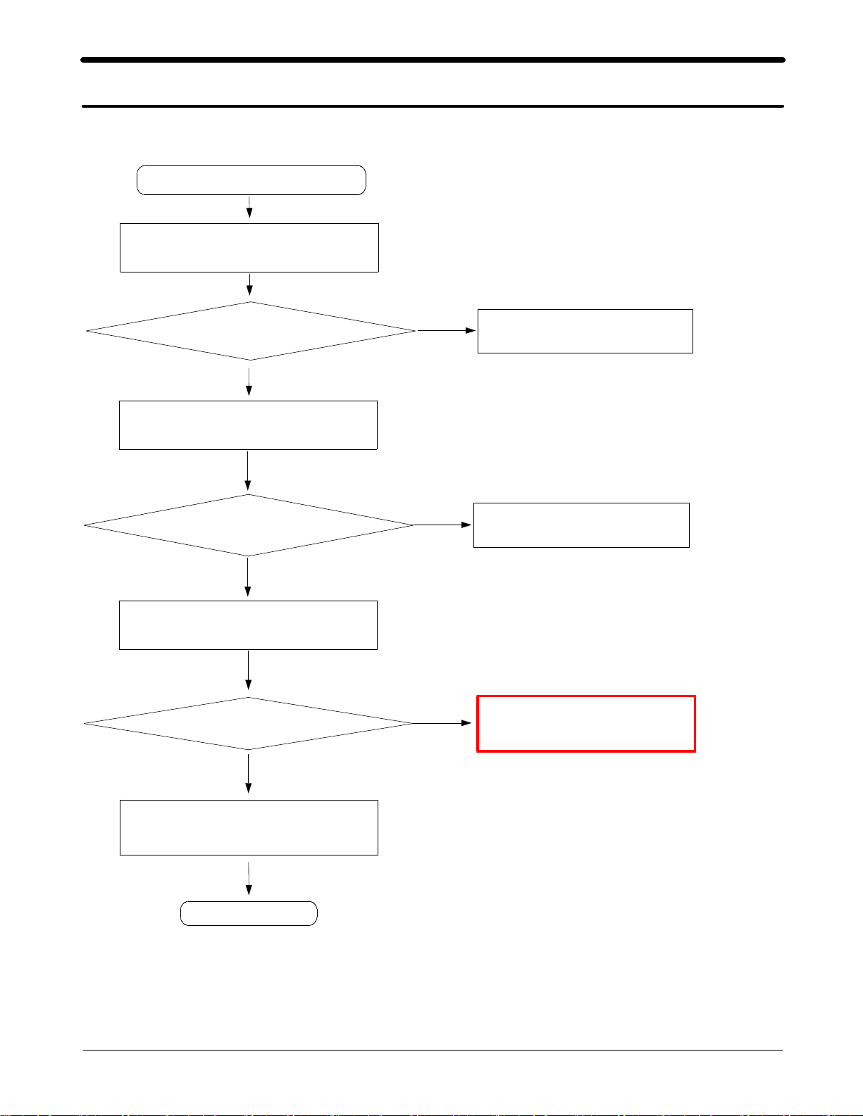
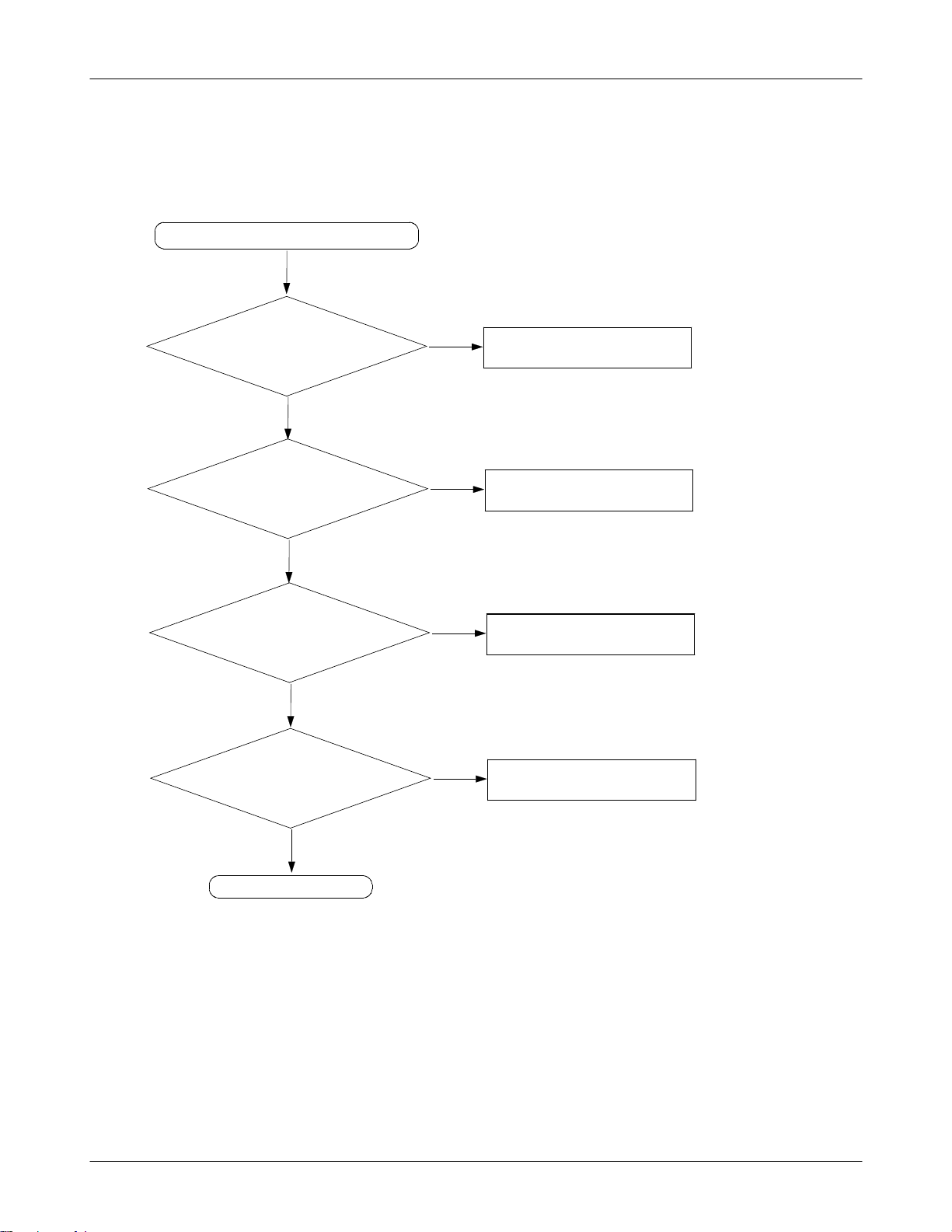
9.
9-1.
Power On
Check the current consumption
Check consumption
Check the voltage
Power On
'
>100
TA801
mA
Yes
>3.1V
'
No
Binary Download
No
Check the battery
Yes
Check the voltage of C451
C451
=3.0V
Yes
Check the initial operation
Yes
END
No
Check the C451, TA801
D401, R426, R427&R428
9-1
SAMSUNG Proprietary-Contents may change without notice
This Document can not be used without Samsung's authorization
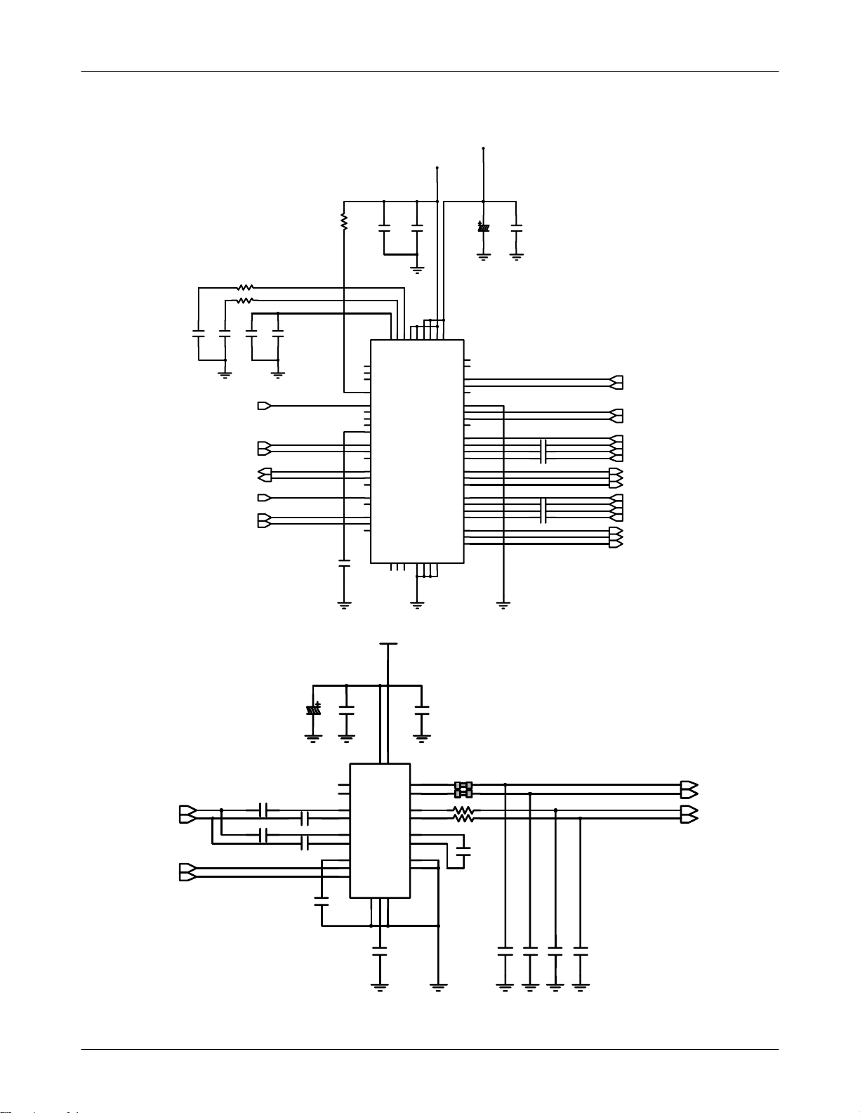
Page 2
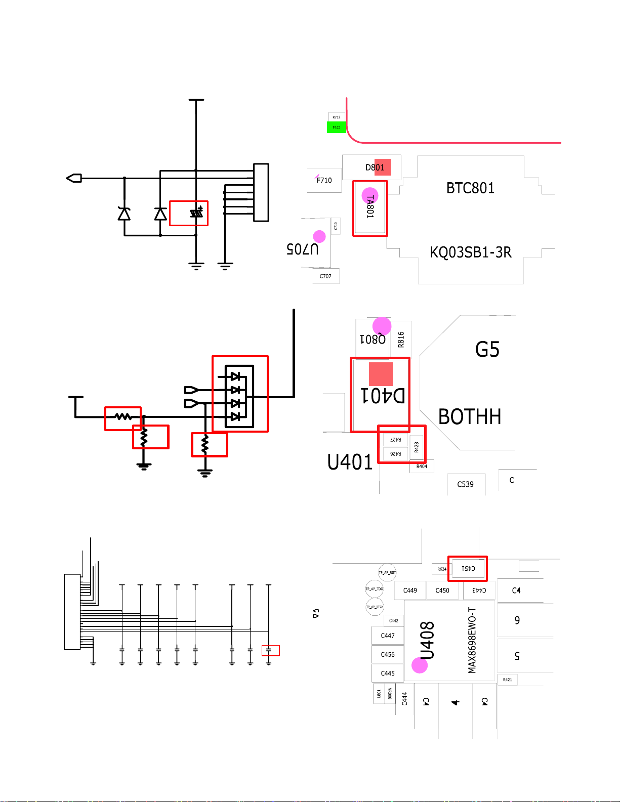
VF
VOVP_5.0V
ZD801
R426
D801
IF_CON_SENSE_USB
VREG_MSMP_2.6V
R427
TA801
VBAT
R428
BTC801
1
1
2
2
3
3
4
NC
5
NC
6
NC
7
NC
D401
1
3
4
2
5
LX1
LX2
LX3
SET1
SET2
SET3
PWREN
PWRON
PWRHOLD BUCK3
MR\
ONO\
RSO\
SCL
SDA
SRAD
LBOB
JIGON
REFBP
U408
F5
VCC_COIN
F1
IN1
G1
IN2
G6
IN3
A2
IN4
C1
IN5
C6
IN6
E2
BUCK1
F2
BUCK2
F4
F6
LDO1
B1
LDO2
A1
LDO3
A3
LDO4
A4
LDO5
A6
LDO6
LDO6
B6
LDO7
D6
LDO8
E6
LDO9
D5
AGND1
E5
AGND2
D1
PGND1
G3
PGND2
G4
PGND3
VALIVE_1.2V_S3C VSD_VCC_3VVOTGI_1.2V_S3C VOTG_3.3V_S3C
LDO1
LDO2
5
0
0
1
C443
VMOVI_3V
LDO3
LDO4
LDO5
C444
C445
C456
VKEY_LED_3.3V
LDO7
C447
VCC_3.0V_PDAVRTC_3.0V_S3C
AP_N_RST_IN
VIBTONE_EN
LDO8
LDO9
C451
C450C449
Page 3
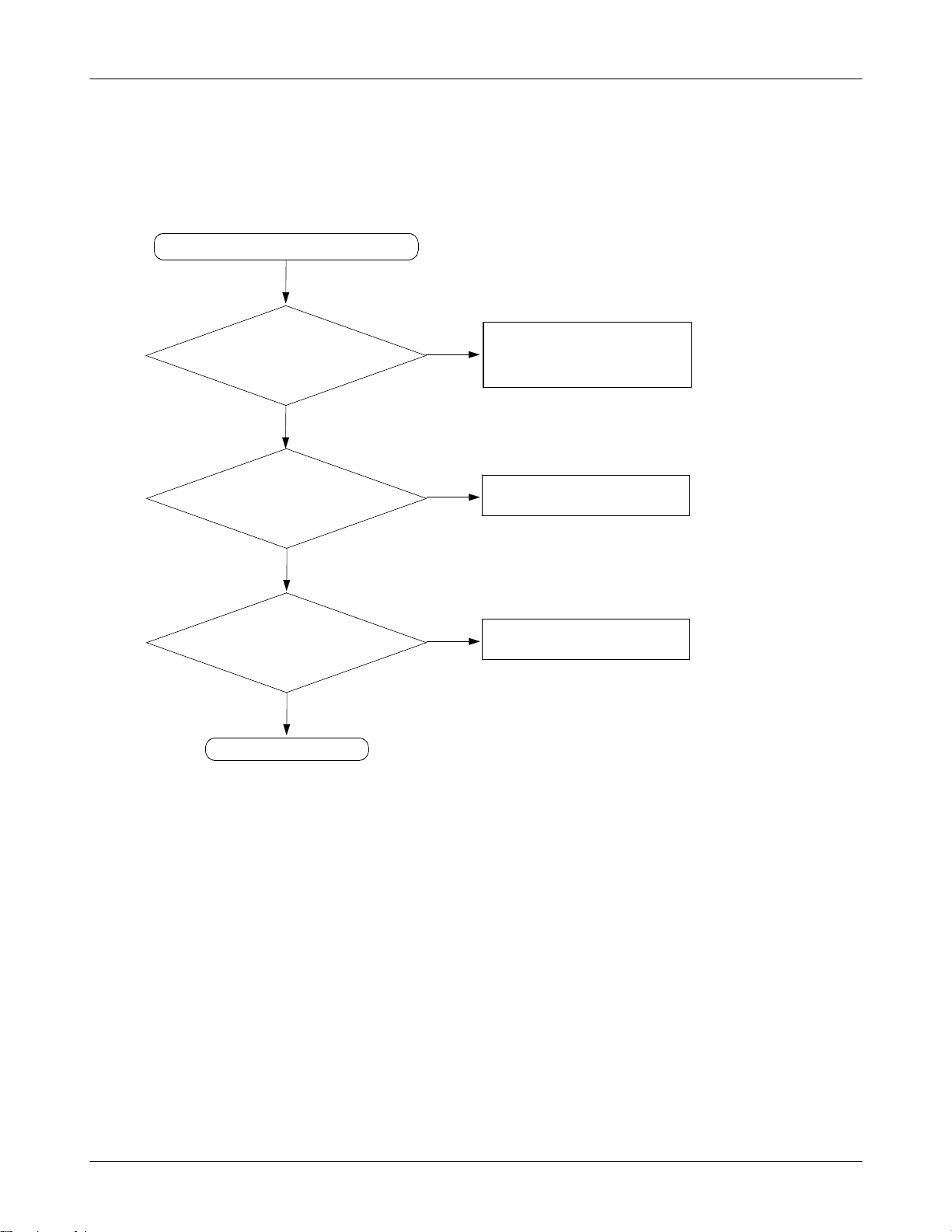
Flow Chart of Troubleshooting
9-2.
initial
Initail Failure
'
TP_PS_HOLD=3.0V
Check the Frequency
R429
= 32.768
C629
=12
'
Yes
Yes
KHz
Yes
MHz
No
No
No
Check UAP601&U410
Check OSC302
Check OSC601
Yes
LCD Display OK?
Yes
Sound operation OK?
Yes
END
No
Check LCD part
No
Check Speaker part
9-3
SAMSUNG Proprietary-Contents may change without notice
This Document can not be used without Samsung's authorization
Page 4

VCC_3.0V_PDA
PS_HOLD
AP_N_RST_IN
VCOIN_3.0V
C342
U410
C
N
11
VCC
VCC
OUT
C
N
62
5
4
12
7
G
1
INA
2
GND
3
INB OUTY
OSC302
1
VIO
C
N
C
N
34
C
C
C
C
N
N
N
N
5
89
10
R436
AP_PS_HOLD
XTAL_12MHZ_IN
XTAL_12MHZ_OUT
R635
1
4
1
0
6
C
S
O
3
2
C628
C629
Page 5
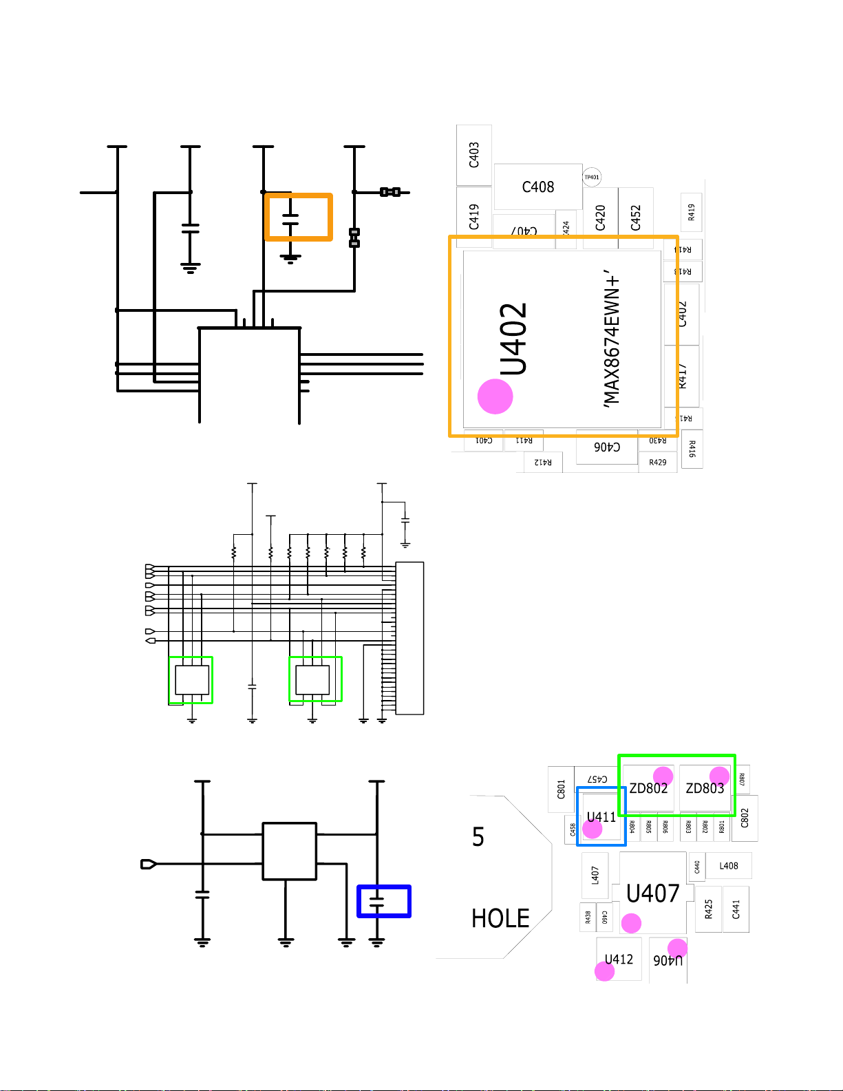
Flow Chart of Troubleshooting
9-3.
T-flash
Initail Failure
'
T-Flash Breakdown
Voltage of C458
There is any signal at
Pin6in T/SIM801
'
NG
No
<3V
No
Yes
Yes
Change T-Flash
Yes
Check U411
No
Check T/SIM801, ZD802&ZD803
Replace T/SIM801
9-5
SAMSUNG Proprietary-Contents may change without notice
This Document can not be used without Samsung's authorization
Page 6
VBAT VREG_RFRX1_2.1V
VREG_USIM_3.0V
VCOIN_3.0V
R439
SD_DAT2_OUT
SD_DAT3_OUT
SD_CMDOUT
SD_CLKOUT
SD_DAT0_OUT
SD_DAT1_OUT
SIM_RST
SIM_CLK
SIM_IO
SD_DET
2
6
D
B
M
M
I
R
S
T
V
V
VCC_3.0V_PDA
R803
OUT1
OUT2
OUT3
OUT4
OUT5
C403
6
1
R408
A6
A5
A7
C7
LDO4
B2
VTFLASH_3V
C801
R807
R806R802 R804
R805
5
4
5
4
3
O
O
O
I
I
I
ZD803
D
2
1
N
O
O
G
I
I
2
3
1
2
3
4
5
6
7
8
9
10
11
12
13
14
15
16
17
18
19
20
21
22
23
24
25
26
27
28
29
30
31
32
T/SIM801
DAT2
CD|DAT3
CMD
VDD
CLK
VSS
DAT0
DAT1
VCC
RST
CLK
RESERVED
GND
VPP
I|O
RESERVED
SW
COMMON
NC
NC
NC
NC
NC
NC
NC
NC
NC
NC
NC
NC
NC
NC
C465
2
7
1
B
C
G
T
S
N
I
T
U
O
A
B
C
B
V
V
A1
IN1
F1
IN2
A4
H5
6
5
5
4
O
O
I
I
ZD802
D
1
N
O
I
G
1
2
U402
IN3
IN4
VREG_USIM_3.0V
R801
4
3
O
I
2
O
I
3
C802
TFLASH_EN
VBAT
C457
4
VDD1VOUT
3
CE
U411
VTFLASH_3V
2
D
GND
N
G
5
C458
Page 7
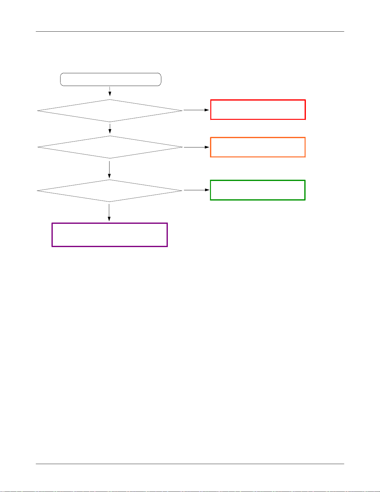
Flow Chart of Troubleshooting
9-4.
SIM
Insert SIM card
SIM CARD Breakdown
No
Voltage of C403
There is any signal at
Pin11in T/SIM801
Replace T/SIM801
<3V
No
Yes
Yes
Change SIM CARD
Yes
Check U402
No
Check T/SIM801, ZD802&ZD803
9-7
SAMSUNG Proprietary-Contents may change without notice
This Document can not be used without Samsung's authorization
Page 8
VBAT VREG_RFRX1_2.1V
VREG_USIM_3.0V
VCOIN_3.0V
R439
C465
2
7
1
B
C
G
T
S
T
U
A
B
B
V
A1
IN1
F1
IN2
A4
H5
U402
IN3
IN4
C403
R408
2
6
D
B
N
M
M
I
I
R
S
O
T
V
C
V
V
A6
OUT1
A5
OUT2
A7
OUT3
C7
LDO4
OUT4
B2
OUT5
VREG_USIM_3.0V
VTFLASH_3V
VCC_3.0V_PDA
C801
SD_DAT2_OUT
SD_DAT3_OUT
SD_CMDOUT
SD_CLKOUT
SD_DAT0_OUT
SD_DAT1_OUT
SIM_RST
SIM_CLK
SIM_IO
SD_DET
6
1
5
O
I
ZD802
1
O
I
R801
R803
R805
R807
R806R802 R804
T/SIM801
1
DAT2
2
CD|DAT3
3
CMD
4
VDD
5
CLK
6
VSS
7
DAT0
8
DAT1
9
VCC
10
RST
11
CLK
12
RESERVED
13
GND
14
VPP
15
I|O
16
RESERVED
17
SW
18
COMMON
19
NC
20
NC
21
NC
4
5
4
3
4
O
O
I
I
6
5
3
5
4
O
O
O
I
I
I
ZD803
D
2
N
O
G
I
2
3
C802
D
2
1
N
O
O
I
G
1
I
2
3
22
NC
23
NC
24
NC
25
NC
26
NC
27
NC
28
NC
29
NC
30
NC
31
NC
32
NC
Page 9
Flow Chart of Troubleshooting
9-5.
Charging
Abnormal Charging operation
Yes
Check IFC801's pin
is about5Vwhen charging
Check U401's pin
is about5Vwhen charging
#1
Yes
#11
Yes
No
Check the TA
No
Check the U802
Check U401's pin
is"LOW" when charging
#4, #11
Yes
END
No
Check the U401
9-9
SAMSUNG Proprietary-Contents may change without notice
This Document can not be used without Samsung's authorization
Page 10
TA_ISET
CHG_EN
12
VUSB_5.0V
10
11
T
N
I
U
O
E
F
A
S
U401
N
E
_
5
4
C413
G
H
C
_
MIN
BATT
_ABO
K
D
O
N
P
_
G
6
VOVP_5.0V
13
GND
14
NC
15
R407
VF
TP_CHG
NC
1
SETI
2
DETBAT
3
ABI
9
8
7
VCC_3.0V_PDA
R404
VBAT
CHG_ING_N
R409
R410
C461
Page 11
Flow Chart of Troubleshooting
9-6.
Bluetooth
Check the connection disable
Yes
Check BT Activation
Yes
Check U202's pin
pin
#39 (1.8
Yes
#15 (
V)
Vbat),
No
Enable BT Function
No
Check the U202
Check BT ANT
Yes
Exchange BT Module(U202)
Yes
END
No
ANT203 reassemble change
9-11
SAMSUNG Proprietary-Contents may change without notice
This Document can not be used without Samsung's authorization
Page 12
ANT203
34
12
L204
BT_PCM_DO
BT_PCM_DI
BT_PCM_CLK
BT_PCM_SYNC
BT_EN
COMBO_38.4M_CLK
CLK32K_COMBO18
C224
C216
TP213
28
27
26
29
25
12
6
3
1
2
4
5
13
38
40
41
42
43
44
R207
AUD_IN
AUD_OUT
AUD_CLK
AUD_FSYNC
BT_EN
BT_DBG
FAST_CLK
SLOW_CLK_IN
NC
NC
NC
NC
NC
NC
NC
NC
NC
NC
NC
D
N
G
7
VBAT
L208
C214
5
3
1
2
T
T
A
N
B
A
V
U202
D
D
D
D
D
D
D
D
D
N
N
N
N
G
G
G
G
2
4
1
4
9
2
2
2
1
1
D
N
N
N
N
N
N
G
G
G
G
G
G
9
8
7
6
0
5
4
4
4
4
5
4
D
D
D
D
D
N
G
1
5
D
D
N
N
N
N
N
N
G
G
G
G
G
G
2
5
4
6
3
5
5
5
5
5
C215
C217
10
HCI_RX
9
HCI_TX
11
HCI_CTS
8
HCI_RTS
SDIO_D1
SDIO_D2
SDIO_D3|SPI_CS
WL_RS232_RX
WL_RS232_TX
WLAN_EN
WLAN_DBG
WLAN_IRQ
CLK_REQ
D
D
N
N
G
G
3
2
4
6
6
6
35
34
33
32
37
36
30
TP218
31
TP219
20
16
TP221
17
18
39
VIO
D
N
G
SDIO_D0|SPI_DOUT
SDIO_CLK|SPI_CLK
SDIO_CMD|SPI_DIN
D
D
D
D
D
N
N
N
N
N
G
G
G
G
G
8
7
1
0
9
5
5
6
6
5
BT_UART_TXD
BT_UART_RXD
BT_UART_RTS
BT_UART_CTS
WLAN_SDIO_D0
WLAN_SDIO_D1
WLAN_SDIO_D2
WLAN_SDIO_D3
WLAN_SDIO_CLK
WLAN_SDIO_CMD
WLAN_EN
WLAN_IRQ
CLK_REQ
VCC_1.8V_PDA
L209
R208
C219
Page 13
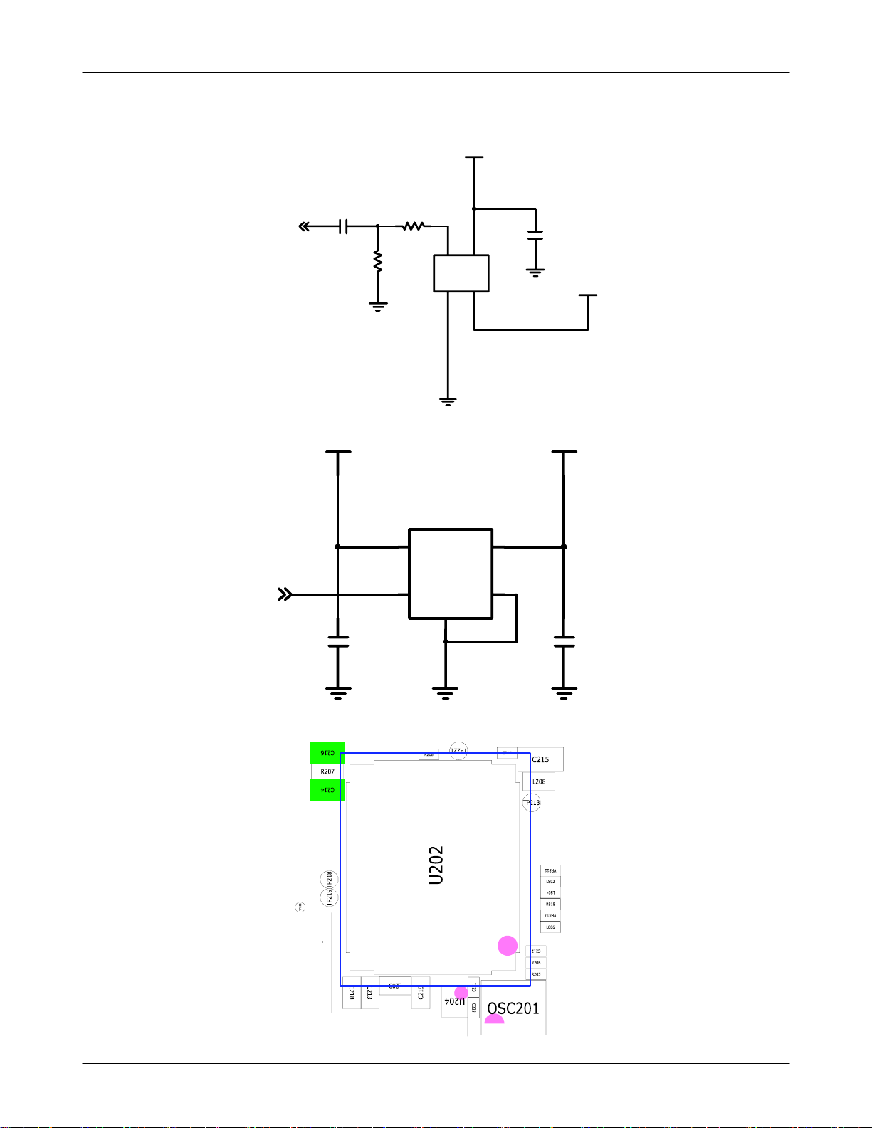
Flow Chart of Troubleshooting
VCOMBO_1.8V
COMBO_38.4M_CLK
CLK_REQ
C212
VBAT
R206
C222
R205
OUT
GND
U204
VDD4VOUT
3
CE
3
OSC201
2
D
N
G
5
4
VDD
SW
1
GND
C211
VCOMBO_1.8V
VCOMBO_1.8V
1
2
C223
9-13
SAMSUNG Proprietary-Contents may change without notice
This Document can not be used without Samsung's authorization
Page 14
Flow Chart of Troubleshooting
9-7.
RECEIVER Working
Recieve does not work
Is there any signal at
C518,C522?
Yes
Is there any siganl at
C730, C731?
Yes
No
Check UCP301
No
Check U502
Is the assemble status if
slide FPCB connector OK?
Yes
Is the assemble status of
receiver OK?
Yes
END
No
Replace slide FPCB connector
No
Resolder or change receiver
9-14
SAMSUNG Proprietary-Contents may change without notice
This Document can not be used without Samsung's authorization
Page 15
Flow Chart of Troubleshooting
R503
R504
C509 C510
C511
CLK19.2M_CODEC
AP_I2S_DO
BT_PCM30_DI
AP_I2S_DI
BT_PCM30_DO
BT_PCM30_SYNC
AP_I2S_SYNC
AUDIO_EN
C512
R502
C524
VCC_3.0V_PDA
VCC_3.0V_PDA
C503
C501
8
9
9
E
D
D
3
T
C
M
D
B
O
O
D
C
C
C
V
O
V
V
T
C
V
D1
SAIN1
C2
SAIN2
C1
SAIN3
I2C
MCKI
MCKO
MDT
MPWR
MUTET
SDTI
SDTIA
SDTIB
SDTO
SDTOA
SDTOB
SYNCA
SYNCB
LRCK
PDN
TEST
U502
C
C
C
N
N
N
3
1
2
C
H5
H4
J4
A1
B1
C8
H1
J8
G1
H2
G9
F2
H9
F1
J3
H3
A9
2
E
2
D
D
V
T
4
S
S
V
2
8
F
D
D
D
D
D
V
V
P
A
S
LOUT1|RCP
LOUT3|LOP
ROUT1|RCN
ROUT3|LON
3
2
S
S
S
S
V
V
7
1
E
H
8
7
J
E
D
D
D
D
V
V
D
A
GPIO1
GPO2
BICK
BICKA
BICKB
CSN|CAD0
CCLK|SCL
CDTI|SDA
CDTO
LIN1||IN1+
LIN2|IN2+
LIN3|IN3+
LIN4|IN4+
LOUT2
RIN1|IN1RIN2|IN2RIN4|IN3RIN4|IN4-
ROUT2
1
S
S
V
8
9
F
B
TA501
C504
8
A
J1
J9
J5
G8
G2
J6
H6
H8
J2
A2
A3
A4
B5
A7
B9
B6
B2
B3
B4
A5
B7
C9
A6
C515
C517
C518
C520
C521
C522
AP_I2S_CLK
BT_PCM30_CLK
AUDIO_SCL
AUDIO_SDA
MIC_P
RADIO_L
EAR_MIC_P
CP_RCV_P
RCV_P
CODEC_OUT_L
CODEC_MIC+
MIC_N
RADIO_R
EAR_MIC_N
CP_RCV_N
RCV_N
CODEC_OUT_R
CODEC_MIC-
CODEC_OUT_L
CODEC_OUT_R
AUDIO_SDA
AUDIO_SCL
C534
C536
TA503
C535
C537
C539
C529
1
5
B
C
D
D
V
RXINRXIN+
INA1
INA2
INB1
INB2
BIAS
SDA
SCL
U503
D
N
G
3
D
P
S
S
V
3
4
A
C
D4
B4
D2
D1
C2
C1
B2
B3
C3
D
D
V
OUT-
OUT+
HPR
HPL
C1N
C1P
D
N
G
P
C530
D5
R517
B5
R519
A1
A2
A4
A5
1
NC
2
NC
C538
C540
C543
C544 C542C541
9-15
SAMSUNG Proprietary-Contents may change without notice
This Document can not be used without Samsung's authorization
SPK_N
SPK_P
EARSPK_R
EARSPK_L
Page 16
Flow Chart of Troubleshooting
9-8.
SPEAKER Working
Speaker does not work
Is the assemble ststus of
speaker module OK?
Yes
Is there any signal at
C534,C535?
Yes
Replace speaker module connector
No
Change speaker module
No
or
Check U502
Is there ant signal at C543,
C544?
Yes
END
No
Check U503
9-16
SAMSUNG Proprietary-Contents may change without notice
This Document can not be used without Samsung's authorization
Page 17

Flow Chart of Troubleshooting
CODEC_OUT_L
CODEC_OUT_R
AUDIO_SDA
AUDIO_SCL
C534
C536
C535
C537
TA503
C539
C529
5
1
C
B
D
D
V
RXINRXIN+
INA1
INA2
INB1
INB2
BIAS
SDA
SCL
U503
D
N
G
3
D
P
S
S
V
4
3
C
A
D4
B4
D2
D1
C2
C1
B2
B3
C3
D
D
V
OUT-
OUT+
HPR
HPL
C1N
C1P
D
N
G
P
C540
C530
R517
D5
B5
R519
A1
A2
A4
A5
1
NC
2
NC
C538
C543
C544 C542C541
SPK_N
SPK_P
EARSPK_R
EARSPK_L
9-17
SAMSUNG Proprietary-Contents may change without notice
This Document can not be used without Samsung's authorization
Page 18

Flow Chart of Troubleshooting
9-9.
MIC Working
Mic does not work
Is there ant signal
at C526?
Yes
No
Is there ant signal
at C526?
Yes
Is there ant signal
at C526?
Yes
No
Replace slide FPCB connector
No
Replace sub key&mic FPCB connector
Change MIC module
The voltage of
R513 is about
Yes
Is there any signal
at R501,R505?
Yes
END
1.6
V?
No
Check the path around MIC bias circuit
No
Check U502
9-18
SAMSUNG Proprietary-Contents may change without notice
This Document can not be used without Samsung's authorization
Page 19

Flow Chart of Troubleshooting
MIC_P
MIC_N
C525
C527
R513
R514
R509
TA502
C526
C519
M_MIC_P
M_MIC_N
ZD502ZD501
CODEC_MIC+
CODEC_MIC-
R501
R505
C502
CP_MIC+
C505
C506
CP_MIC-
C513
9-19
SAMSUNG Proprietary-Contents may change without notice
This Document can not be used without Samsung's authorization
Page 20

Flow Chart of Troubleshooting
9-10.
Earphone
Speaker does not work
Is the condition if IFC800
Does Mic of headset work?
OK?
Yes
Yes
No
No
Replace or chagne IFC800
Check mic path and bias circuit
Does ear phone if headset
work?
Yes
END
No
Check ear speaker path
9-20
SAMSUNG Proprietary-Contents may change without notice
This Document can not be used without Samsung's authorization
Page 21

Flow Chart of Troubleshooting
VMIC_2.8V
C528
R515
AP_D+
AP_D-
EAR_R_TV
EAR_L_TV
EARSPK_L
EARSPK_R
EAR_MIC+
TV_OUT
V_AUDIO_L
V_AUDIO_R
IF_TXD
IF_RXD
JTAG_TXD
JTAG_RXD
L813
L814
L501
VBAT
C806
VTA_5.0V
B1
DP_HOST
C1
DM_HOSTC2I2C_SCL
D2
ID_BYPASS
B3
AUDIO_L
C4
AUDIO_R
B4
MIC
D4
VIDEO
C3
V_AUDIO_L
D3
V_AUDIO_R
E2
TXD
E1
RXD
TA504
C532
VUSB_5.0V VCC_3.0V_PDA
1
4
2
5
D
A
A
A
T
T
N
O
I
I
A
U
_
D
B
O
S
D
_
V
U
V
S
B
U
V
B
V
B2
I2C_SDA
D5
ID_CON
C5
DP_CON
B5
DM_CON
U802
D
N
G
5
E
A1
INTB
A3
CHG_DET
E4
JIG
E3
BOOT
C
C
N
N
2
1
L812
0603
FM_ANT
TP801
1
Q801
R516
C531
IF_nINT
TA_ISET
JTAG_IF_CON_SENSE
BOOT_MODE
VBAT
R815
2
3
C803
R816
C533
AP_SCL_3.0V
AP_SDA_3.0V
ID
L809
1
VBUS
DM
2
DP
3
USB_ID
D
N
G
7
IF_CON_SENSE_USB
EAR_MIC_PEAR_MIC+
EAR_MIC_N
VBATVTA_5.0V
IFC801
NC
13
NC
12
NC
11
NC
10
NC
9
NC
8
S2
7
S1
6
5
5
4
4
3
3
2
2
1
1
C804
6
5
NC
4
NC
U803
5
0
0
1
C805
9-21
SAMSUNG Proprietary-Contents may change without notice
This Document can not be used without Samsung's authorization
Page 22

Flow Chart of Troubleshooting
9-11.
Key Data Input
Press Key
Volume Key
NG
?
No
Camera Key
NG
?
No
Yes
Yes
Volume Key
Breakdown?
Camera Key
FPCB
Breakdown?
Yes
Change volume key
Yes
Change camera Key
Hold key NG?
Yes
No
Hold Key
Breakdown?
Yes Yes
Power Key NG?
No
Power Key Breakdown?
Yes Yes
Qwerty Key NG?
No No
especially register in key colume
END
(
Domesheet
Breakdown?
check the element related
lines)
Yes
Change Hold Key
Change Key
Change Domesheet
9-22
SAMSUNG Proprietary-Contents may change without notice
This Document can not be used without Samsung's authorization
Page 23

Flow Chart of Troubleshooting
9-12. 5M
Camera part
Camera Function does not work?
5M
Yes
Check camera FPCB and
Replace the New Camera
connector
Yes
C712
=1.2V
C708
=3.0V
C713
=1.8V
C709
=2.8V
Yes
Check the R711&R712
Yes
Yes
END
No
Re-connect the camera FPCB
No
Check U705
No
Check Mclk&Pclk
9-23
SAMSUNG Proprietary-Contents may change without notice
This Document can not be used without Samsung's authorization
Page 24

VBAT
Flow Chart of Troubleshooting
C706
VCAM_CORE_1.2V
B3
IRQ_N
C3
FM_SCL
FM_SDA
CAM_PWR_EN
TP703
L701
C712
SCL
C4
SDA
D3
DVS
D2
FB
E2
EN
E3
SW
VCAM_CORE_1.2V
VCAM_HOST_3.0V VBAT
VCAM_DVDD_1.8V
CAM_SDA CAM_SCL
CAM_5M_RST_n
CAM_VSYNC CAM_HSYNC
CAM_MCLK
CAM_M(1)
CAM_M(3)
CAM_M(5)
CAM_M(7)
C707
4
2
1
4
A
A
D
E
1
2
T
B
T
N
N
N
I
I
I
A
V
V
V
B
B4
V
LDO1
A3
LDO2
A1
LDO3
C1
LDO4
E1
LDO5
U705
B2
DEFSEL
C2
IDSEL
B
D
D
N
N
C
C
N
N
G
G
1
2
1
4
B
D
VCAM_AF_2.8V
VCAM_AVDD_2.8V
R711
VCAM_AVDD_2.8V
VCAM_HOST_3.0V
C708
HEA702
11
33
55
77 88
99
1111 1212
13
13 14
15
15 16
17
17 18
19
19
21
21
232424
23
252626
25
27
27 28
29
29
313232
31
333434
33
NC
NC NC
35 36NC37
C709
38
14
16
18
20
22
28
30
22
VCAM_SVDD_1.8V
44
66
1010
20
22
30
VCAM_DVDD_1.8V
C710 C711C713
VCAM_SVDD_1.8V
R712
VCAM_AF_2.8V
CAM_5M_STBY
CAM_PCLK
CAM_M(0)
CAM_M(2)
CAM_M(4)
CAM_M(6)
C715
C721
C714
9-24
SAMSUNG Proprietary-Contents may change without notice
This Document can not be used without Samsung's authorization
Page 25

Flow Chart of Troubleshooting
9-13.
CIF Camera part
CIF Camera Function does not work?
Yes
Check camera FPCB and
Check camera FPCB and
Replace the New Camera
connector
connector
C104
C105
END
Yes
=1.8V
=3.0V
Yes
Yes
Yes
No
No
No
No
Re-connect the slide FPCB
Re-connect the camera FPCB
Check U101
Replace the New slide FPCB
9-25
SAMSUNG Proprietary-Contents may change without notice
This Document can not be used without Samsung's authorization
Page 26

Flow Chart of Troubleshooting
VCIF_AVDD_3.0V
VBAT
U101
1
2
CAM_PWR_EN CAM_PWR_EN
C103
3
VIN
GND
EN2
VOUT1
VOUT2
EN1
GND
7
VCIF_DVDD_1.8V
6
5
4
C104
C105
VCIF_IO_3.0V
R104
VCIF_AVDD_3.0VVCIF_IO_3.0VVCIF_DVDD_1.8V
HEA100
1
CAM_HSYNC
CAM_VSYNC
CAM_SDA
CAM_PCLK
CAM_D(2)
CAM_D(1)
CAM_D(0)
CAM_MCLK CAM_D(5)
1
3
3
5
5
7
7
9
9
11
11
13 13 14 14
15
15 1616
17 17 18 18
19
19
2121
C
C
N
N
3
4
2
2
2
10
12
2
4
4
6
6
8
8
10
12
CAM_CIF_RST_n
CAM_CIF_STBY
CAM_SCL
CAM_D(3)
CAM_D(7)
CAM_D(6)
2020
22
22
C
C
N
N
6
5
2
2
CAM_D(4)
9-26
SAMSUNG Proprietary-Contents may change without notice
This Document can not be used without Samsung's authorization
Page 27

Flow Chart of Troubleshooting
9-14.
GPS part
Yes
Yes
Yes
No
Enable GPS funtion
No
Check L202, L203, F202
Yes
Yes
END
No
Check MSM6290
No
Resolder error parts
9-27
SAMSUNG Proprietary-Contents may change without notice
This Document can not be used without Samsung's authorization
Page 28

ANT201
1
1
2
2
ANT202
Flow Chart of Troubleshooting
VREG_RFRX2_2.7V
1
1
2
2
GLNA_ON
R202
L202
C204
L203
R203
C
2
1
0
N
C220
A
2
0
2
R
F
2
0
2
R203
2
T
2
0
C220
C210
F
2
0
1
C208
L
2
0
6
F201
1
4
OUT
IN
G
2G3G5
C208
L206
F202
5
2
D
D
|
D
S
V
1
RF_IN
FILT_OUT
D
D
N
N
G
G
3
6
C206
4
RX_GPS
G1
4
0
L20 2 L203
2
C
0
6
N
T
2
0
1
A
2
C
9-28
SAMSUNG Proprietary-Contents may change without notice
This Document can not be used without Samsung's authorization
Page 29

Flow Chart of Troubleshooting
9-15.
GSM850 Receiver
RX ON
Sector PWR=-50dBm
MOD101 Pin
>= -60
MOD101 Pin
12,13
2
dBm
Yes
Yes
No
No
Resolder RFS101,C1024,L101
Check MOD101
Truth Table
Pin3:LOW
Pin4:HIGH
Pin5:HIGH
Pin6:LOW
Yes
Resolder or change
MOD101
U101
Pin
50,51
dBm
>= -75
Yes
Change U101&UCP301
No
Resolder or change L102,L103,L104
9-29
SAMSUNG Proprietary-Contents may change without notice
This Document can not be used without Samsung's authorization
Page 30

Flow Chart of Troubleshooting
9-16.
GSM850 Transmitter
TX ON
PCL5level)
(
Cell Power
Normal Condition Catch the
channel
MOD101 Pin
>= 5
MOD101 Pin
>= 5
:-40
dBm
dBm
dBm
2
No
11
Yes
Yes
Check MOD101
Truth Table
Pin3:HIGH
Pin4:LOW
Pin5:LOW
Pin6:LOW
Resolder RFS101,C1024,L101
No
U101 Pin
>= 5
Check U101&UCP301
dBm
END
55
No
YES
Resolder or change MOD101
Yes
Resolder or change C120
9-30
SAMSUNG Proprietary-Contents may change without notice
This Document can not be used without Samsung's authorization
Page 31

Flow Chart of Troubleshooting
9-17.
GSM900 Receiver
RX ON
Sector PWR=-50dBm
MOD101 Pin
>= -60
MOD101 Pin
14,15
U101
Pin
>= -75
2
dBm
Yes
Yes
48,49
dBm
No
No
No
Resolder RFS101,C1024,L101
Check MOD101
Truth Table
Pin3:LOW
Pin4:LOW
Pin5:HIGH
Pin6:LOW
Resolder or change L105,L106,L107
Yes
Resolder or change
MOD101
Yes
Change U101&UCP301
9-31
SAMSUNG Proprietary-Contents may change without notice
This Document can not be used without Samsung's authorization
Page 32

Flow Chart of Troubleshooting
9-18.
GSM900 Transmitter
TX ON
PCL5level)
(
Cell Power
Normal Condition Catch the
channel
MOD101 Pin
>= 5
MOD101 Pin
>= 5
:-40
dBm
dBm
dBm
2
No
11
No
Yes
Yes
Check MOD101
Truth Table
Pin3:HIGH
Pin4:LOW
Pin5:LOW
Pin6:LOW
Resolder RFS101,C1024,L101
YES
Resolder or change MOD101
U101 Pin
>= 5
Check U101&UCP301
dBm
END
55
No
Yes
9-32
Resolder or change C115
SAMSUNG Proprietary-Contents may change without notice
This Document can not be used without Samsung's authorization
Page 33

Flow Chart of Troubleshooting
9-19.
DCS Receiver
RX ON
Sector PWR=-50dBm
MOD101 Pin
>= -60
MOD101 Pin
16,17
>= -70
U101
Pin
>= -75
2
dBm
Yes
dBm
Yes
46,47
dBm
No
No
No
Resolder RFS101,C1024,L101
Check MOD101
Truth Table
Pin3:LOW
Pin4:LOW
Pin5:LOW
Pin6:LOW
Resolder or change L108,L109,L110
Yes
Resolder or change
MOD101
Yes
Change U101&UCP301
9-33
SAMSUNG Proprietary-Contents may change without notice
This Document can not be used without Samsung's authorization
Page 34

Flow Chart of Troubleshooting
9-20.
DCS Transmitter
TX ON
PCL5level)
(
Cell Power
Normal Condition Catch the
channel
MOD101 Pin
dBm
>= 5
MOD101 Pin
dBm
>= 5
:-40
No
dBm
2
9
Yes
Yes
Check MOD101
Truth Table
Pin3:HIGH
Pin4:HIGH
Pin5:LOW
Pin6:LOW
Resolder RFS101,C1024,L101
No
U101 Pin
>= 5
Check U101&UCP301
dBm
END
56
No
Yes
YES
Resolder or change MOD101
Resolder or change C118
9-34
SAMSUNG Proprietary-Contents may change without notice
This Document can not be used without Samsung's authorization
Page 35

Flow Chart of Troubleshooting
9-21.
PCS Receiver
RX ON
Sector PWR=-50dBm
MOD101 Pin
>= -60
MOD101 Pin
18,19
2
dBm
Yes
Yes
No
No
Resolder RFS101,C1024,L101
Check MOD101
Truth Table
Pin3:LOW
Pin4:HIGH
Pin5:LOW
Pin6:LOW
Yes
Resolder or change MOD101
U101
Pin
44,45
dBm
>= -75
Yes
Change MOD101&UCP301
No
Resolder or change L111,L112,L113
9-35
SAMSUNG Proprietary-Contents may change without notice
This Document can not be used without Samsung's authorization
Page 36

Flow Chart of Troubleshooting
9-22.
PCS Transmitter
TX ON
PCL5level)
(
MOD101 Pin
dBm
>= 5
MOD101 Pin
dBm
>= 5
U101 Pin
dBm
>= 5
No
56
No
2
9
Yes
Yes
Check MOD100
Truth Table
Pin3:HIGH
Pin4:HIGH
Pin5:LOW
Pin6:LOW
Resolder RFS101,C1024,L101
YES
Resolder or change MOD101
Yes
Resolder or change C118
No
Check U101&UCP301
END
9-36
SAMSUNG Proprietary-Contents may change without notice
This Document can not be used without Samsung's authorization
Page 37

C1024
Flow Chart of Troubleshooting
RFS101
G
4
2AC1G3
L129
R103
ANT101
1
2
1
2
GSM850_900_OUT
DPCS_OUT
ANT_SEL0
ANT_SEL1
ANT_SEL2
ANT_SEL3
R113
R115
TX_IM
TX_IP
TX_QM
TX_QP
DAC_REF
R114
R116
11
C114
C121
VREG_FEM_2.85V
MOD101
7
2
T
D
N
D
A
GSM850|900TX GSM850RX
9
GSM1800|1900TX
3
VC1
4
VC2
5
VC3
6
VC4
V
GSM850RX
GSM900RX
GSM900RX
GSM1800RX
GSM1800RX
GSM1900RX
GSM1900RX
G
G
G
G
G
0
3
4
1
8
1
2
2
UMTS1
UMTS2
UMTS3
C110
RX_GSM850_N
RX_GSM850_P
RX_EGSM900_N
RX_EGSM900_P
RX_DCS1800_N
RX_DCS1800_P
RX_PCS1900_N
RX_PCS1900_P
TRX_WCDMA2100
TRX_WCDMA900
TRX_WCDMA1900
RFOUT_W2100
RFOUT_W1900
C111
ANT102
1
2
1
2
L103
L106
L108
L109
L111
L112
L101
L102
L104
0
L105
L107
L110
L113
C109
C119
C122
12
13
14
15
16
17
18
19
20
21
22
C128
C130
C141
C112
C113
C115
RFOUT_W900
C118
C120
RFOUT_DCS_PCS
RFOUT_G850_EGSM
R104
1
2
3
4
5
6
7
8
9
10
11
12
13
14
15
16
17
1
7
C
N
VDDA2
TCXO
VDDA1
VDDA1
VTUNE1
VDDA1
VDDA2
VDDA2
VTUNE_GPS
VDDA1
PRX_QP
PRX_QN
PRX_IN
PRX_IP
DRX_QP
DRX_QN
DRX_IP
8
1
9
8
7
6
5
4
0
6
6
6
7
S
C
G
A
N
U
I
L
B
S
R
_
_
D
X
N
T
G
3
6
6
6
6
F
P
P
N
I
E
Q
Q
_
R
_
_
X
I
X
X
T
_
T
T
C
A
D
9
2
0
1
5
6
6
6
2
2
2
N
I
A
A
A
_
D
D
D
X
D
D
D
T
V
V
V
5
8
7
6
5
5
5
5
3
2
1
2
1
T
T
T
T
T
U
U
U
U
U
O
O
O
O
O
_
_
_
_
_
F
F
F
F
F
R
R
R
R
R
_
_
_
_
_
B
B
B
B
B
L
L
H
H
H
U101
M
P
N
N
I
N
I
_
T
X
D
C
|
R
B
N
D
S
9
0
1
2
2
2
1
E
A
M
A
N
D
D
D
U
D
T
D
D
V
V
V
V
1
4
3
2
2
2
2
2
_
X
2
2
N
M
A
A
O
_
D
D
_
B
F
D
D
W
V
R
V
8
7
6
5
2
2
2
2
P
M
M
P
I
_
X
M
_
B
W
9
2
B
B
B
B
H
H
L
L
X
X
X
X
R
R
R
R
P
P
P
P
W
W
W
W
2
3
1
0
3
3
3
3
4
2
3
5
5
5
2
1
PDET_IN
A
A
D
D
D
D
V
V
GCELL_INN
GCELL_INP
EGSM_INN
EGSM_INP
DCS_INN
DCS_INP
GPCS_INN
GPCS_INP
VDDA2
GPS_IN
WDRXLB
WDRXHB1
WDRXHB2
WPRXSE1
T
U
VDDA2
O
_
2
WPRXSE2
E
S
X
WPRXSE1_OUT
R
P
W
4
3
C126
51
50
49
48
47
46
45
44
43
42
41
40
39
38
37
36
35
9-37
SAMSUNG Proprietary-Contents may change without notice
This Document can not be used without Samsung's authorization
PWR_DET
RX_GSM850_N
RX_GSM850_P
RX_EGSM900_N
RX_EGSM900_P
RX_DCS1800_N
RX_DCS1800_P
RX_PCS1900_N
RX_PCS1900_P
RX_GPS
Page 38

Flow Chart of Troubleshooting
C142
8
5
C
1
1
3
2
1
9
6
C125
1
0
1
2
8
0
1
1
L
C
C124
1
C
C123
C
3
1
2
C
3
1
3
C
8
1
L
1
1
2
2
C141
0
L113
6
L
1
1
1
1
R
L
1
0
9
T
U
L110
C130
L
1
0
8
R
L107
L
1
0
6
C128
1
4
L
0
L
1
0
3
C122
L
1
0
2
L
1
0
5
F
1
0
7
C
1
1
1
0
0
1
L
0
1
1
2
0
7
1
C
1
D
O
M
9-38
SAMSUNG Proprietary-Contents may change without notice
This Document can not be used without Samsung's authorization
Page 39

Flow Chart of Troubleshooting
9-23.
WCDMA
RX ON
Sector PWR
MOD101 Pin
>= -60
MOD101 Pin
>= -70
F107 Pin
>= -75
=-50
dBm
Yes
dBm
Yes
dBm
2100
2
20
6
dBm
Receiver
No
No
No
Resolder RFS101,C1024,L101
Check MOD101
Truth Table
Pin3:LOW
Pin4:LOW
Pin5:LOW
Pin6:HIGH
Resolder C1010,C1011,L127
Yes
Resolder or change MOD101
Yes
F107 Pin
>= -75
Change MOD101,F107,UCP301
1
dBm
Yes
No
Resolder or change
C1016,C1018,L128
9-39
SAMSUNG Proprietary-Contents may change without notice
This Document can not be used without Samsung's authorization
Page 40

Flow Chart of Troubleshooting
9-24.
WCDMA
UE Target Power24dBm)
(
2100
MOD101 Pin
MOD101 Pin
Transmitter
TX ON
dBm
>= 15
dBm
>= 15
No
F107 Pin
dBm
>= 15
Yes
Yes
Check MOD101
Resolder RFS101,C1024,L101
Truth Table
Pin7:LOW
Pin6:LOW
Pin8:LOW
Pin9:HIGH
YES
Resolder or change
Resolder C1010,C1011,L127
MOD101
2
No
20
Yes
6
NO
U104 Pin
dBm
>= 15
NO
U104 Pin
dBm
>= 15
NO
U101 Pin
dBm
>= 15
Check U101
59
Yes
9
2
Yes
Resolder or change
Yes
Resolder or change F107,C1017,C1019
Resolder or change F106
U104
C1020
,
END
9-40
SAMSUNG Proprietary-Contents may change without notice
This Document can not be used without Samsung's authorization
Page 41

Flow Chart of Troubleshooting
9-25.
WCDMA
RX ON
Sector PWR
MOD101 Pin
>= -60
MOD101 Pin
>= -70
F105 Pin
>= -75
=-50
dBm
Yes
dBm
Yes
dBm
1900
2
22
6
dBm
Receiver
No
No
No
Resolder RFS101,C1024,L101
Check MOD101
Truth Table
Pin3:LOW
Pin4:LOW
Pin5:LOW
Pin6:HIGH
Resolder C176,C177,L123
Yes
Resolder or change MOD101
Yes
F105 Pin
>= -75
Change MOD101,F105,UCP301
1
dBm
Yes
No
Resolder or change
L124,C187,C188
9-41
SAMSUNG Proprietary-Contents may change without notice
This Document can not be used without Samsung's authorization
Page 42

Flow Chart of Troubleshooting
9-26.
WCDMA
UE Target Power24dBm)
(
1900
MOD101 Pin
MOD101 Pin
Transmitter
TX ON
dBm
>= 15
dBm
>= 15
No
F105 Pin
dBm
>= 15
Yes
Yes
Check MOD101
Resolder RFS101,C1024,L101
Truth Table
Pin7:LOW
Pin6:LOW
Pin8:LOW
Pin9:HIGH
YES
Resolder or change
Resolder C176,C177,L123
MOD101
2
No
22
Yes
6
NO
U103 Pin
dBm
>= 15
NO
U104 Pin
dBm
>= 15
NO
U101 Pin
dBm
>= 15
Check U101
59
Yes
9
2
Yes
Resolder or change
Yes
Resolder or change F105,C183,C198
U104
Resolder or change F104
END
9-42
SAMSUNG Proprietary-Contents may change without notice
This Document can not be used without Samsung's authorization
Page 43

Flow Chart of Troubleshooting
9-27.
WCDMA
RX ON
Sector PWR
MOD101 Pin
>= -60
MOD101 Pin
>= -70
F103 Pin
>= -75
=-50
dBm
Yes
dBm
Yes
dBm
6
900
dBm
2
21
Receiver
No
No
No
Resolder RFS101,C1024,L101
Check MOD101
Truth Table
Pin3:LOW
Pin4:HIGH
Pin5:LOW
Pin6:HIGH
Resolder C152,L116
Yes
Resolder or change MOD101
Yes
F103 Pin
>= -75
Change MOD101,F103,UCP301
1,8
dBm
Yes
No
Resolder or change
C157,C169,L120
9-43
SAMSUNG Proprietary-Contents may change without notice
This Document can not be used without Samsung's authorization
Page 44

Flow Chart of Troubleshooting
9-28.
WCDMA
UE Target Power24dBm)
(
900
Transmitter
TX ON
MOD101 Pin
MOD101 Pin
>= 15
>= 15
dBm
dBm
No
F103 Pin
dBm
>= 15
Yes
Yes
Check MOD101
Resolder RFS101,C1024,L101
Truth Table
Pin7:LOW
Pin6:LOW
Pin8:LOW
Pin9:HIGH
YES
Resolder or change
Resolder C152,L116
MOD101
2
No
22
Yes
6
NO
U102 Pin
dBm
>= 15
NO
U102 Pin
dBm
>= 15
NO
U100 Pin
dBm
>= 15
Check U101
58
Yes
7
4
Yes
Resolder or change
Yes
Resolder or change F102,L122,L118,C174
F102
Resolder or change F102
END
9-44
SAMSUNG Proprietary-Contents may change without notice
This Document can not be used without Samsung's authorization
Page 45

C1024
Flow Chart of Troubleshooting
RFS101
G
4
2AC1G3
L129
R103
ANT101
1
2
1
2
GSM850_900_OUT
DPCS_OUT
ANT_SEL0
ANT_SEL1
ANT_SEL2
ANT_SEL3
L116
R113
R115
R114
R116
C152
VREG_FEM_2.85V
7
2
T
D
N
D
A
G
G
G
1
0
8
1
TRX_WCDMA900
V
G
3
2
11
GSM850|900TX GSM850RX
9
GSM1800|1900TX
3
VC1
4
VC2
5
VC3
6
VC4
MOD101
GSM850RX
GSM900RX
GSM900RX
GSM1800RX
GSM1800RX
GSM1900RX
GSM1900RX
UMTS1
UMTS2
UMTS3
G
4
2
C109
C119
C122
12
13
14
15
16
17
18
19
20
21
22
C128
C130
C141
L109
L103
L105
L106
L108
L111
L112
L101
C1010
L102
L104
0
L107
L110
L113
C1011
L127
C110
RX_GSM850_N
RX_GSM850_P
RX_EGSM900_N
RX_EGSM900_P
RX_DCS1800_N
RX_DCS1800_P
RX_PCS1900_N
RX_PCS1900_P
TRX_WCDMA2100
TRX_WCDMA900
TRX_WCDMA1900
C111
TRX_WCDMA2100
ANT102
1
2
1
2
6
L120
C157
C169
WCDMA_RXP_900
L121
WCDMA_RXM_900
6
ANT
1
3
RX
TX
8
RX
G
G
G
G
G
9
7
4
2
5
F107
ANT
3
G
2
4
1
RXTX
C1018
G
G
G
G
G
9
5
8
7
L128
C1016
RTR_W2100
F103
L123
L124
C177
C188
C187
TRX_WCDMA1900
WCDMA_RX_1900
C143
3
OUT
1
G2G
IN
OUT 4
5
F101
L115
C146
WCDMA_RXM_2100
WCDMA_RXP_2100
C176
F105
6
ANT
TX
3
RX
1
G
G
G
G
G
2
45
7G89
9-45
SAMSUNG Proprietary-Contents may change without notice
This Document can not be used without Samsung's authorization
Page 46

Flow Chart of Troubleshooting
C
C
1
1
6
7
7
1
F102
6
0
6
7
1
1
C
C
C151
C150
7
1
4
C
L122
L
1
1
6
U
1
0
2
L118
3
0
C1023
C179
0
2
1
L
C1009
C1014
C1012
C1022
1
F
C157
1
2
1
L
C169
U104
7
5
U103
1
C
1
5
2
C
1
0
1
5
F106
C
1
8
5
C
1
0
1
3
C
1
8
1
F
1
0
4
C182
C186
C195
C196
C
1
1
6
T
0
R
1
1
3
C
C
1
1
1
3
7
8
R
L107
L
L
L
1
1
1
0
0
6
5
C128
D
R
R
1
1
1
1
5
4
1
0
8
1
0
1
L
C153
1
9
8
4
4
1
1
C
C
C
1
5
4
C
1
6
2
8
0
1
R
C
1
4
C
1
4
5
7
5
1
1
1
L
C
C
1
6
5
L
1
1
9
R
L
1
1
1
0
4
5
C142
8
8
1
6
C125
1
0
1
L
1
2
C
C124
C
1
0
C123
1
1
F
1
0
9
1
0
1
C
7
8
1
C
7
L
1
2
4
1
8
C
8
F
1
0
1
0
1
C
C
1
5
6
9
0
1
R
C1025
C144
6
0
1
R
C159
C158
C160
C
1
6
3
C
1
6
1
6
3
C
1
0
0
8
C
1
0
2
0
C
1
0
1
7
C
8
1
6
7
1
2
C
C
1
6
4
C
1
7
4
C
L
1
1
5
1
0
1
F
C
1
4
5
0
C
0
1
7
R
1
1
C
1
2
7
8
R110
C
1
9
7
0
C
C
1
1
8
9
3
8
5
3
9
C140
8
5
1
C
1
1
3
2
1
9
C
2
C
1
3
C
1
3
3
C
1
0
L
1
2
7
C
1
7
7
C
1
7
6
L
1
2
3
L
1
1
2
2
9
L113
C141
0
1
2
7
0
1
6
C
1
0
2
4
8
1
1
R
R
1
U
L110
L
L
1
1
1
0
1
9
C130
1
C
C
C
R
1
1
9
O
R
1
1
6
0
4
L
1
0
3
C122
1
0
2
L
1
M
C
1
1
0
0
1
3
L
1
0
2
9
1
1
C
C
C
9-46
SAMSUNG Proprietary-Contents may change without notice
This Document can not be used without Samsung's authorization
Page 47

Flow Chart of Troubleshooting
9-29
Charging Part
Abnormal charging part
Check IFC801's pin
is about
Check the U401's pin
is about5Vwhen charging?
when charging?
5.0V
Yes
Yes
Yes
#1
#11
No
No
Check the TA
Check the U802
Check the U401's pin
#10is"
Low" when charging?
Yes
END
#4,
No
check the U401
9-47
SAMSUNG Proprietary-Contents may change without notice
This Document can not be used without Samsung's authorization
Page 48

Flow Chart of Troubleshooting
TA_ISET
CHG_EN
GND
NC
NC
SETI
DETBAT
ABI
VUSB_5.0V
12
C413
10
11
T
N
G
I
U
H
O
C
E
_
F
A
S
U401
BATT
_ABO
K
D
O
N
N
P
E
G
_
_
6
4
5
VOVP_5.0V
13
14
15
R407
VF
1
2
3
TP_CHG
R409
MIN
9
8
7
R410
VCC_3.0V_PDA
R404
VBAT
CHG_ING_N
C461
9-48
SAMSUNG Proprietary-Contents may change without notice
This Document can not be used without Samsung's authorization
Page 49

Flow Chart of Troubleshooting
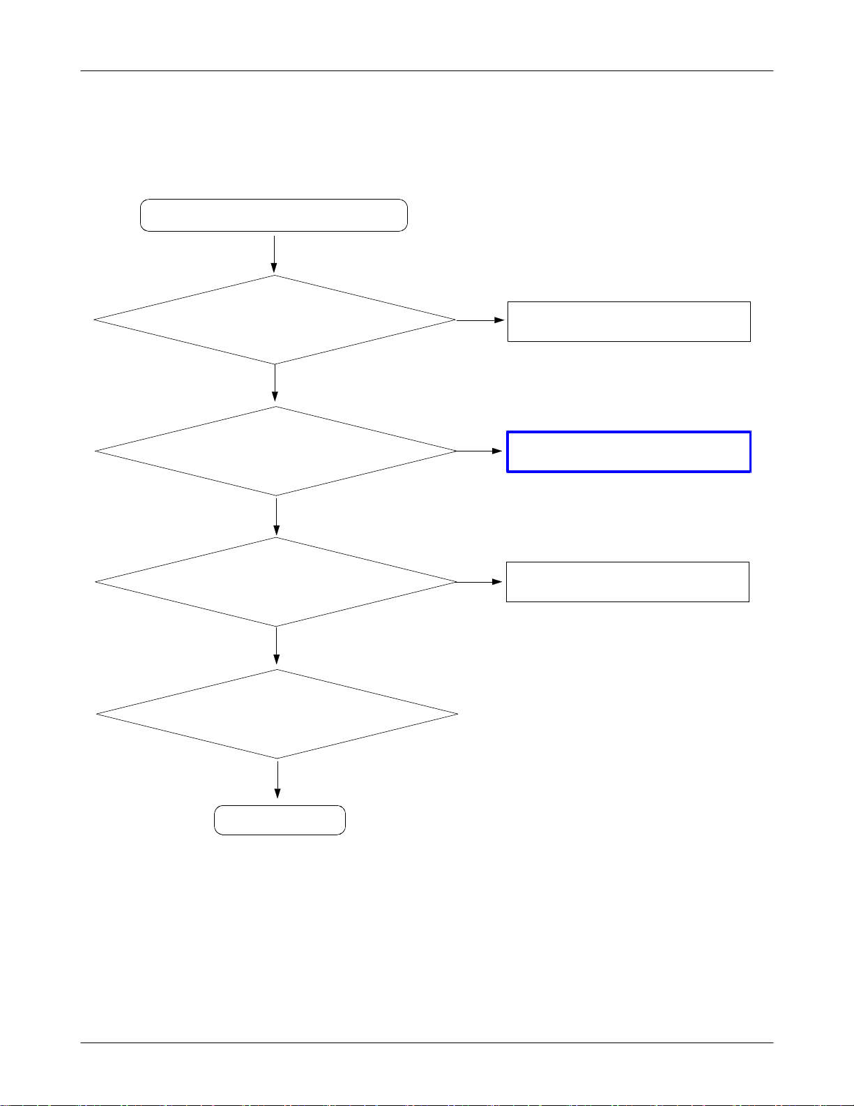
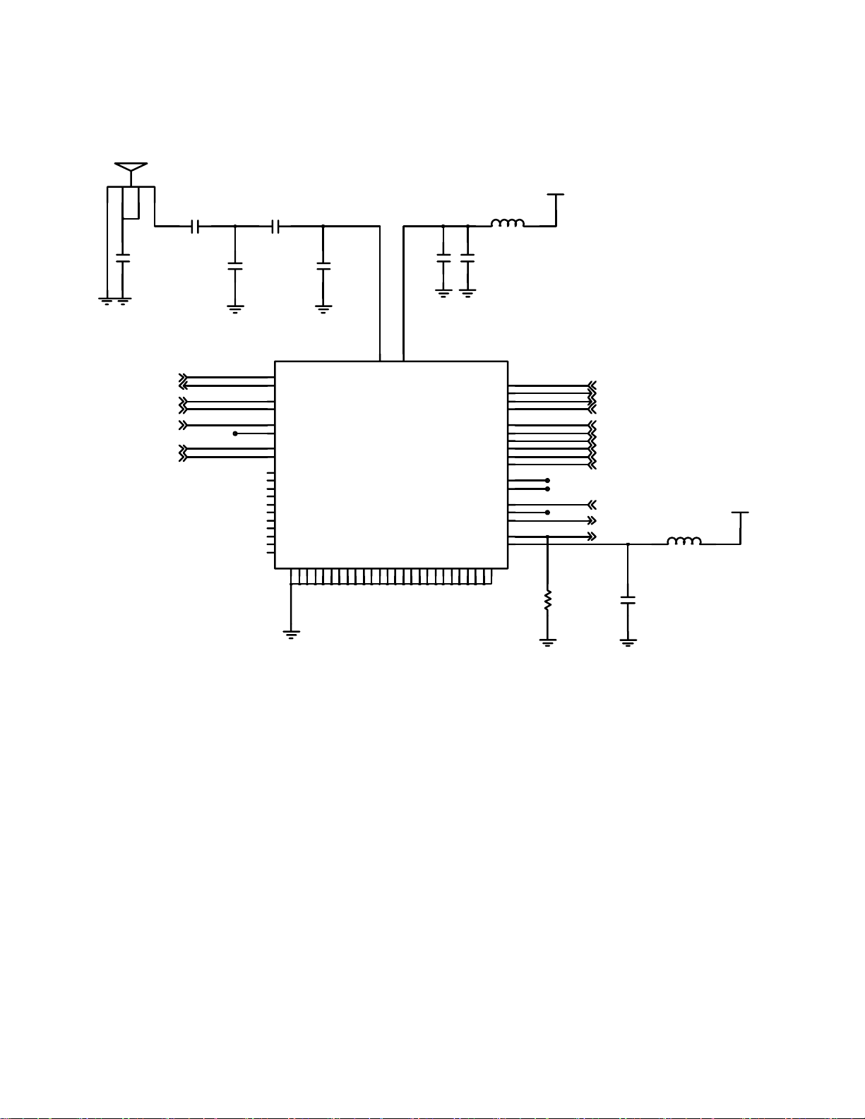
9-30.
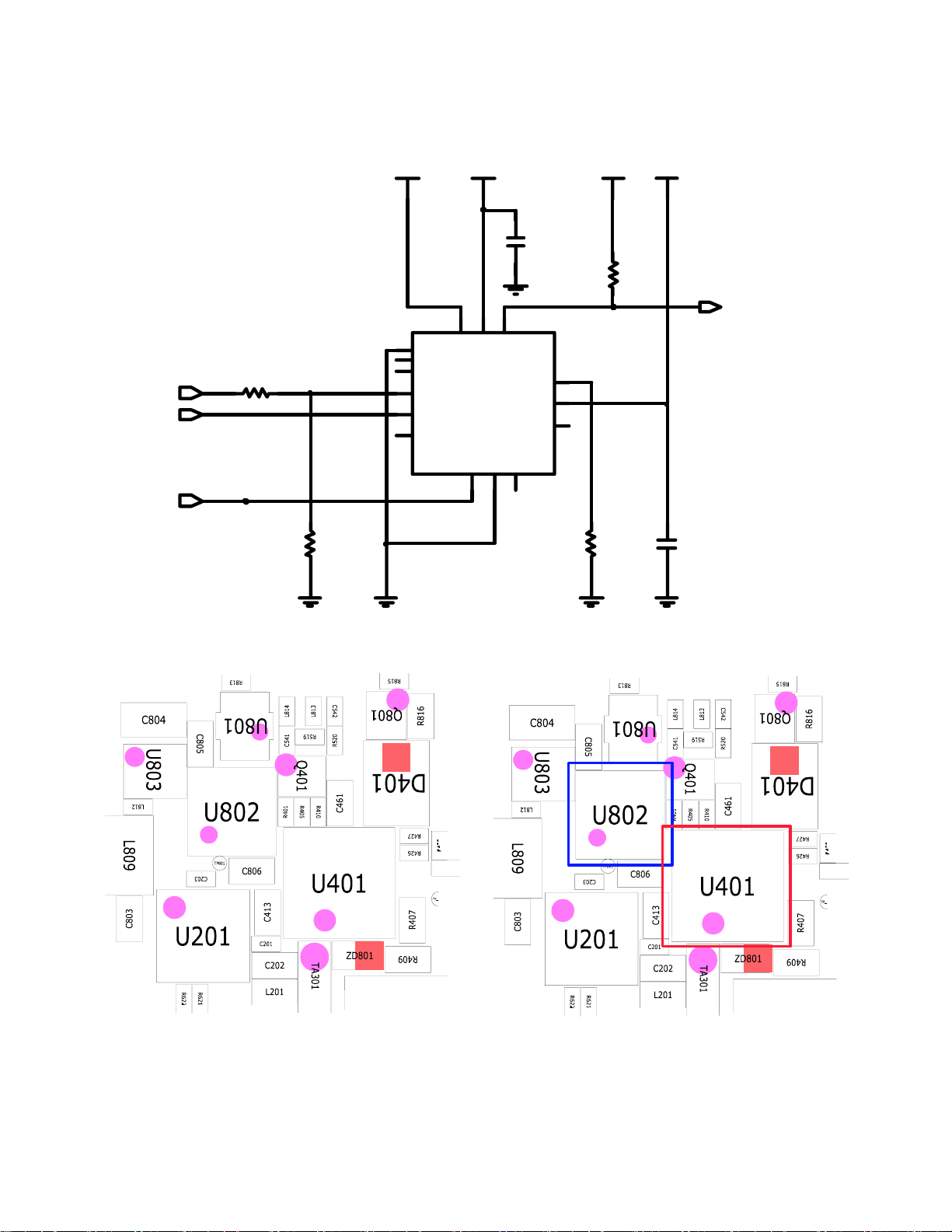
Radio part
check VCC_3.0V_PDA on
Radio does not work
Yes
L201
Is it
V?
3.0
Yes
Resolder the U201
END
Resolder or Replace L201
9-49
SAMSUNG Proprietary-Contents may change without notice
This Document can not be used without Samsung's authorization
Page 50

Flow Chart of Troubleshooting
9-50
SAMSUNG Proprietary-Contents may change without notice
This Document can not be used without Samsung's authorization
Page 51

Block Diagrams
7.
7-1.
Main Block Diagram
7-1
SAMSUNG Proprietary-Contents may change without notice
This Document can not be used without Samsung's authorization
Page 52

PCB Diagrams
8.
8-1
SAMSUNG Proprietary-Contents may change without notice
This Document can not be used without Samsung's authorization
Page 53

PCB Diagrams
8-2
SAMSUNG Proprietary-Contents may change without notice
This Document can not be used without Samsung's authorization
 Loading...