

Samsung B7510 Service Manual
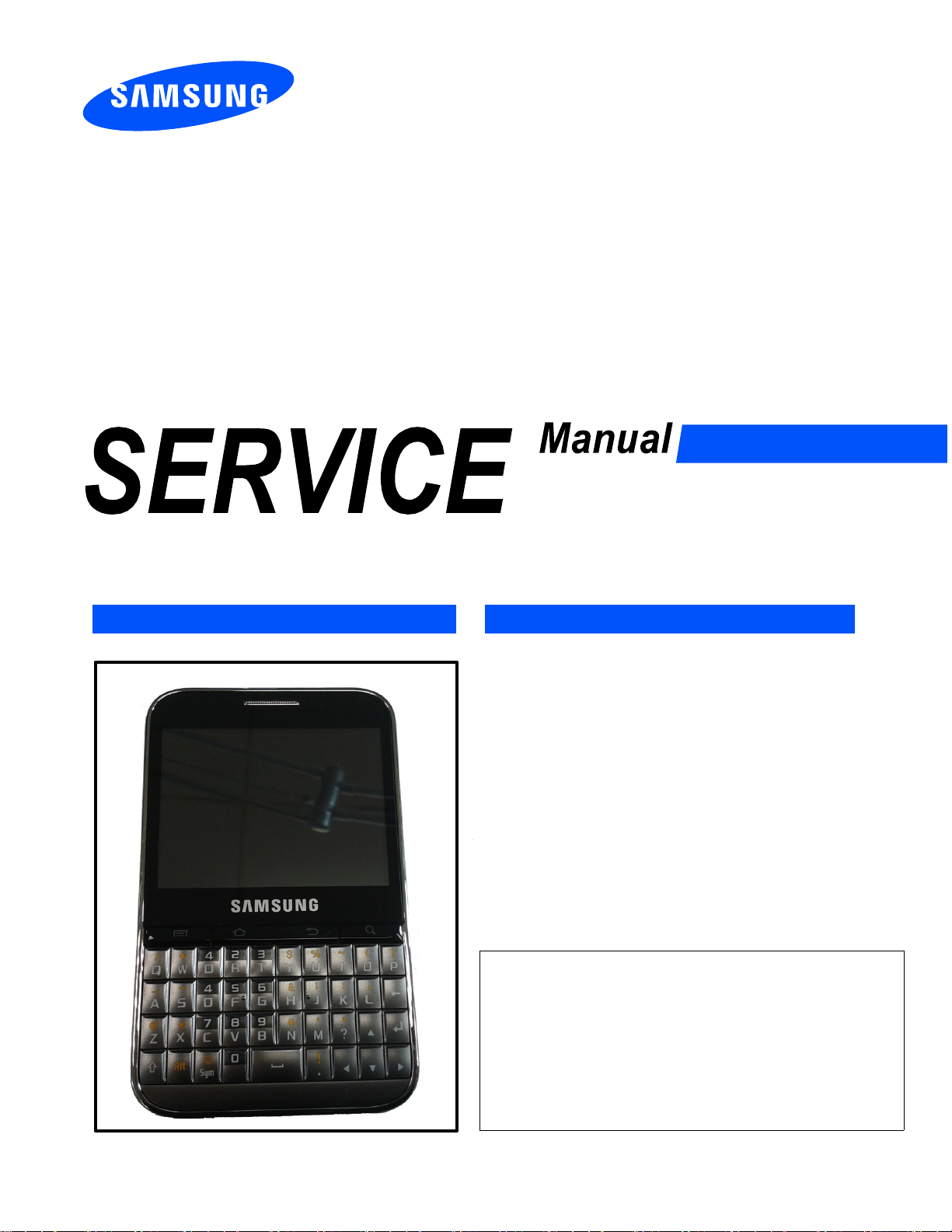
GSM TELEPHONE
GT-B7510
GSM TELEPHONE
CONTENTS
Safety Precautions
1.
Specification
2.
Product Function
3.
Exploded View and Parts list
4.
MAIN Electrical Parts List
5.
Level1Repair
6.
Level2Repair
7.
Level3Repair
8.
Reference data
9.
Notice
All functionality, features, specifications and other
product information provided in this document inclu
ding, but not limited to, the benefits, design, pricing,
components, performance, availability, and capabiliti
es of the product are subject to change without
-
notice or obligation. Samsung reserves the right to
make changes to this document and the product
described herein, at anytime, without obligation on
Samsung to provide notification of such change.
:

Safety Precautions
1.
Repair Precaution
1-1.
Repair in Shield Box, during detailed tuning. Take specially care of tuning or test, because
―
specipicty of cellular phone is sensitive for surrounding interference(RF noise).
Be careful to useakind of magnetic object or tool, because performance of parts is damaged by
―
the influence of magnetic force.
Surely useastandard screwdriver when you disassemble this product, otherwise screw will be
―
worn away.
Useathicken twisted wire when you measure level.
―
thicken twisted wire has low resistance, therefore error of measurement is few.
A
Repair after separate Test Pack and Set because for short danger(for example an overcurrent
―
and furious flames of parts etc) when you repair board in condition of connecting Test Pack and
tuning on.
Take specially care of soldering, because Land of PCB is small and weak in heat.
―
Surely tune on/off while using AC power plug, becausearepair of battery charger is dangerous
―
when tuning ON/OFF PBA and Connector after disassembling charger.
Don't use as you pleases after change other material than replacement registered on SEC System.
―
Otherwise engineer in charge isn't charged with problem that you don't keep this rules.
1-1
SAMSUNG Proprietary-Contents may change without notice
This Document can not be used without Samsung's authorization

Safety Precautions
ESD(Electrostatically Sensitive Devices) Precaution
1-2.
Several semiconductor may be damaged easily by static electricity. Such parts are called by ESD
Electrostatically Sensitive Devices), for example IC,BGA chip etc. Read Precaution below.
(
You can prevent from ESD damage by static electricity.
Remove static electricity remained your body before you touch semiconductor or parts with
―
semiconductor. There are ways that you touch an earthed place or wear static electricity prevention
string on wrist.
Use earthed soldering steel when you connect or disconnect ESD.
―
Use soldering removing tool to break static electricity.,otherwise ESD will be damaged by static
―
electricity.
Don't unpack until you set up ESD on product. Because most of ESD are packed by box and
―
aluminum plate to have conductive power,they are prevented from static electricity.
You must maintain electric contact between ESD and place due to be set up until ESD is
―
connected completely to the proper place oracircuit board.
1-2
SAMSUNG Proprietary-Contents may change without notice
This Document can not be used without Samsung's authorization
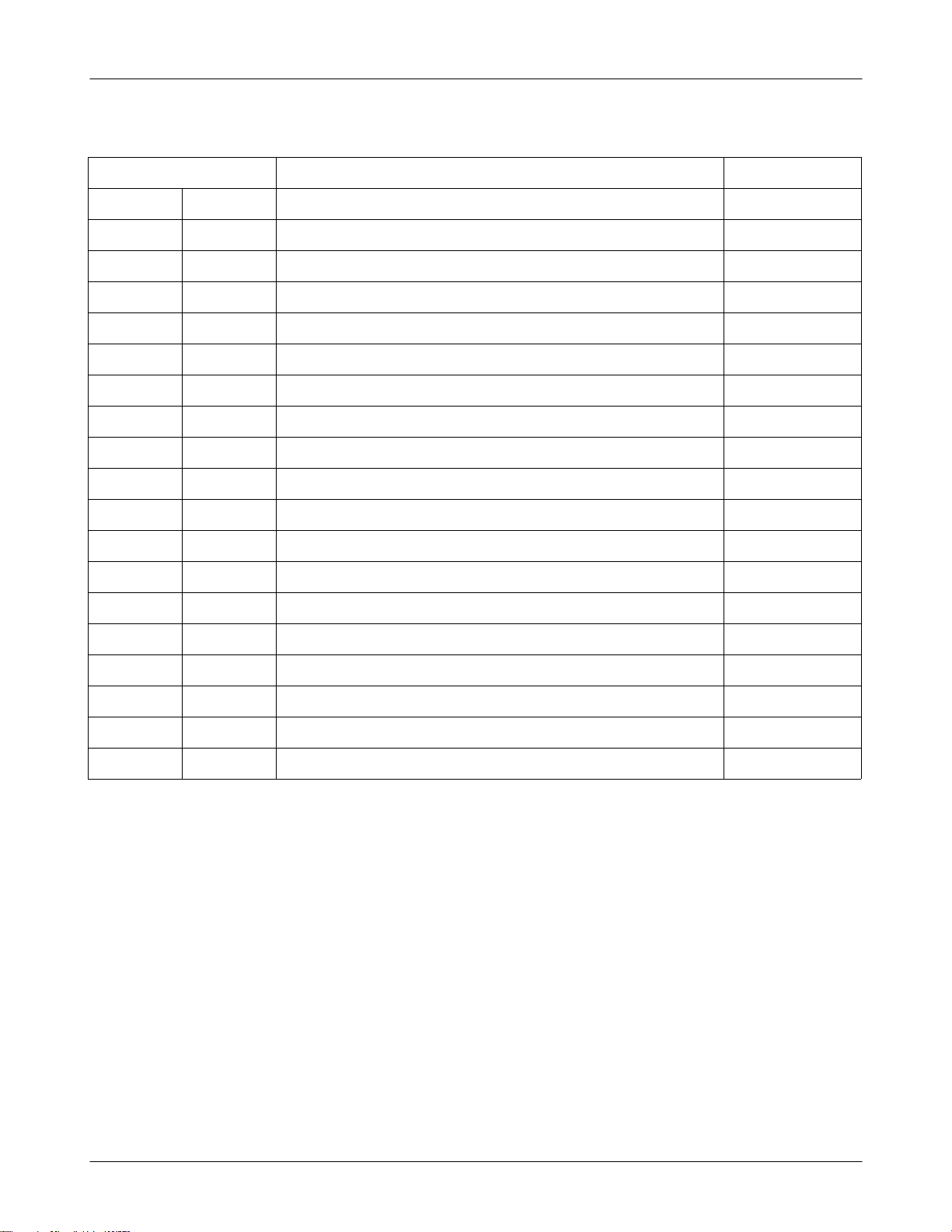
Specification
2.
GSM General Specification
2-1.
GSM850
Phase 1
Freq.
Band[MHz]
Uplink/Downlin
k
ARFCN range 128~251
Tx/Rx spacing 45MHz 45MHz 95MHz 80MHz 190MHz 45MHz
Mod. Bit rate/
Bit Period
Time Slot
Period/Frame
Period
824~849
869~894
270.833kbp
s
3.692us
576.9us
4.615ms
EGSM 900
Phase 2
880~915
925~960
0~124 &
975~1023
270.833kbp
s
3.692us
576.9us
4.615ms
DCS1800
Phase 1
1710~1785
1805~1880
512~885 512~810
270.833kbp
s
3.692us
576.9us
4.615ms
PCS1900
1850~1910
1930~1990
270.833kbp
s
3.692us
576.9us
4.615ms
WCDMA
2100
1922~1977
2112~2167
UL:9612~98
88DL:10562
~10838
3.84Mcps 3.84Mcps
FrameLengt
h:
10ms
Slotlength:
0.667ms
WCDMA900
880~915
925~960
UL:2712~28
63,DL:2937
~3088
FrameLengt
h:
10ms
Slotlength:
0.667ms
Modulation 0.3GMSK 0.3GMSK 0.3GMSK 0.3GMSK
MS Power
Power Class
Se
nsitivity
TDMA Mux 8 8 8 8
Cell Radius 35Km 35Km 2Km 2Km 2Km 2Km
33dBm~5dBm33dBm~5dBm30dBm~0dBm30dBm~0dBm24dBm~-
5pcl ~
19pcl
-102dBm -102dBm -100dBm -100dBm -106.7dBm -106.7dBm
pcl
5
~19
pcl0pcl
2-1
~15
pcl0pcl
~15
QPSKHQPSKQPSKHQPS
24dBm~-
pcl
50dBm
max+24dB
3(
m)
8
50dBm
max+24dB
3(
K
m)
8
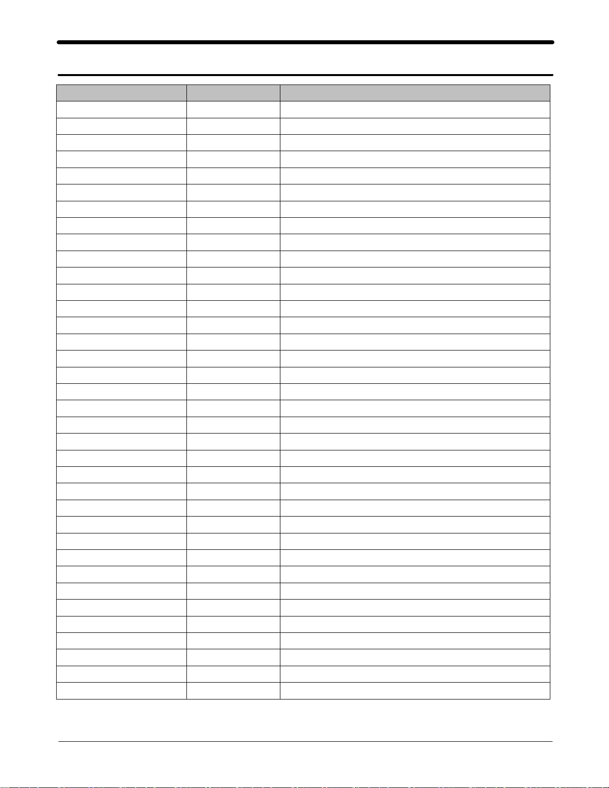
Specification
GSM Tx Power Class
2-2.
TX Power
control
GSM850
level
533±2
631±2
729±2
827±2
925±2
10 23±2
11 21±2
12 19±2
dBm
dBm
dBm
dBm
dBm
dBm
dBm
dBm
TX Power
control
EGSM900
level
533±2
631±2
729±2
827±2
925±2
10 23±2
11 21±2
12 19±2
dBm
dBm
dBm
dBm
dBm
dBm
dBm
dBm
TX Power
control
DCS1800
level
030±3
128±3
226±3
324±3
422±3
520±3
618±3
716±3
dBm
dBm
dBm
dBm
dBm
dBm
dBm
dBm
TX Power
control
PCS1900
level
030±3
128±3
226±3
324±3
422±3
520±3
618±3
716±3
dBm
dBm
dBm
dBm
dBm
dBm
dBm
dBm
13 17±2
14 15±2
15 13±2
16 11±3
17 9±3
18 7±3
19 5±3
dBm
dBm
dBm
dBm
dBm
dBm
dBm
13 17±2
14 15±2
15 13±2
16 11±3
17 9±3
18 7±3
19 5±3
dBm
dBm
dBm
dBm
dBm
dBm
dBm
2-2
814±3
912±4
10 10±4
11 8±4
12 6±4
13 4±4
14 2±5
15 0±5
dBm
dBm
dBm
dBm
dBm
dBm
dBm
dBm
814±3
912±4
10 10±4
11 8±4
12 6±4
13 4±4
14 2±5
15 0±5
dBm
dBm
dBm
dBm
dBm
dBm
dBm
dBm

Operation Instruction and Installation
3.
Main Function
GoogleAndroid OS
-
Size:
-
Band:GSM QUAD BAND GSM850/900/1800/1900(Release:R99)
-
BAND:HSDPA
-
3
-
LCD:
-
1350
-
3.5
-
Micro USB/ Power, Data
-
Wi-Fi
-
Bluetooth v3.0
-
USB v2.0 High Speed,
-
A-GPS
-
FM w/RDS
-
input:QWERTY Key, C-Type single TSP
-
Audio:mp3, ogg, aac, mid, xmf, rtttl, imy, rtx, ota, amr, wav, mxmf
-
Image:bmp, gif, jpg, png, wbmp, agif
-
Video:MPEG4, H.263, H.264,3gp, mp4
-
B/B: MSM7227 turbo
-
PMIC: MAX8899
-
Tranceiver: RTR6285
-
PAM: SKY77554(2G)
-
RF7201(3G Dual)
-
Intenna:Carrier type
-
LCD:
-
MEMORY:4G+3G
-
108.6
Mega pixel AF Camera,
2.8"
mA standard Battery
pi Earjack/ Earphone
802.11
2.8"
x66.7x10.65
7.2M
LQVGA TFT
b/g/n
LQVGA TFT
2.2
Froyo
B1/B8
800M
1/5"
CMOS
3-1
SAMSUNG Proprietary-Contents may change without notice
This Document can not be used without Samsung's authorization
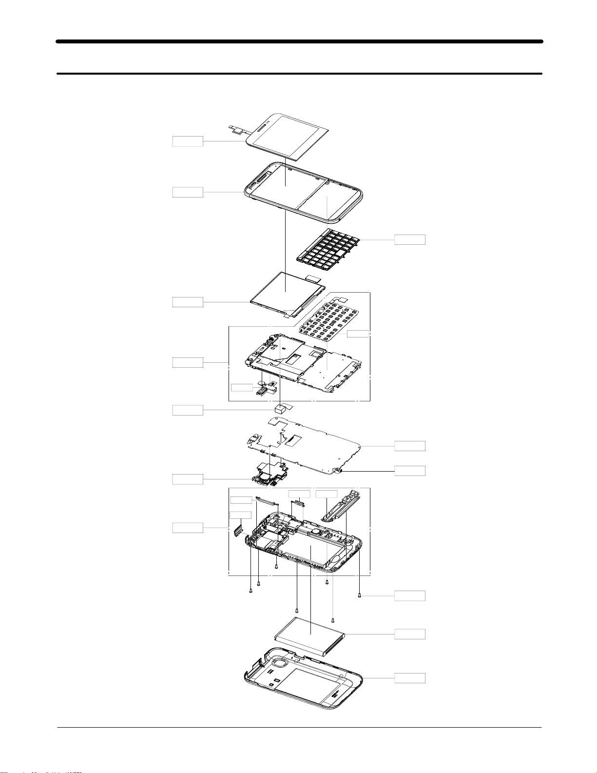
Exploded View and Parts List
4.
Cellular phone Exploded View
4-1.
QME03
QFR01
QLC01
QKP01
QME01
QLB01
QCA01
QSP01
QRE01
QAR01
QVO01
QRF06
QMP01
QMI01
QCK01 QAN02
QCR67
QBA01
QBC00
4-1
SAMSUNG Proprietary-Contents may change without notice
This Document can not be used without Samsung's authorization
Exploded View and Parts List
Cellular phone Parts list
4-2.
Design LOC Description SEC CODE
QCR67 SCREW-MACHINE
6001-002083
QMI01 MICROPHONE-ASSY-GT-B7510 GH30-00722A
QBA01 INNER BATTERY PACK-EB494358VU,GT-S5830,L GH43-03504A
QSP01 MODULE-SPK+SIM S/C GH59-10724A
QME03 TOUCH/PANEL-GT-B7510 GH59-10728A
QMP01 A/S ASSY-PBAMAIN(COMM)GT-B7510 GH82-05631A
QLC01 ELA MODULE-LCD MODULE(GT-B7510) GH96-05085A
QCA01 ASSY CAMERA-3M AF MODULE(GT-B7510 GH96-05091A
QFR01 ASSY CASE-FRONT GH98-18418A
QBC00 ASSY COVER-BATT GH98-18420A
QKP01 ASSY KEYPAD-QWERTY GH98-18421A
QLB01 ASSY BRACKET-LCD GH98-18430A
QME01 KEY FPCB-QWERTY KEY(GT-B7510) GH59-10713A
QAR01 ASSY ETC-RCV&EAR JACK ASSY GH59-10737A
QRE01 ASSY CASE-REAR GH98-18419A
QAN02 INTENNA-GTB7510 MAIN GH42-02892A
QRF06 PMO COVER-DC USB GH72-61733A
QCK01 PMO KEY-POWER HOLD GH72-61734A
QVO01 PMO KEY-VOLUME GH72-61735A
4-2
SAMSUNG Proprietary-Contents may change without notice
This Document can not be used without Samsung's authorization
MAIN Electrical Parts List
5.
Design LOC SEC CODE Description
D401
D501
ZD400,ZD600,ZD601
ZD508
D502
ZD401,ZD402,ZD403
ZD500,ZD501,ZD502
ZD506,ZD511,ZD513
ZD514,ZD606
D400,D500
Q500
TR400
U301
U300
U601
U501
U103
PAM100
U500
U401
U403
U503
U402
U400
U603
U100
U200
U201
UCP300
U600
U602
TH300
ZD602,ZD603,ZD604
R337
R101,R323,R510,R532
R610
0403-001870
0404-001172
0406-001286
0406-001329
0406-001431
0406-001459
0406-001459
0406-001459
0406-001459
0407-001002
0504-001138
0505-002341
0801-003200
0801-003265
1001-001385
1001-001645
1201-003057
1201-003210
1202-001068
1203-004776
1203-005298
1203-006331
1203-006346
1203-006732
1204-003112
1205-003297
1205-004076
1205-004113
1205-004180
1209-002023
1209-002030
1404-001221
1405-001298
2007-000137
2007-000138
2007-000138
DIODE-ZENER
DIODE-SCHOTTKY
DIODE-TVS
DIODE-TVS
DIODE-TVS
DIODE-TVS
DIODE-TVS
DIODE-TVS
DIODE-TVS
DIODE-ARRAY
TR-DIGITAL
FET-SILICON
IC
IC
IC
IC
IC
IC
IC
IC
IC
IC
IC
IC
IC
IC
IC
IC
IC
IC
IC
THERMISTOR
VARISTOR
R-CHIP
R-CHIP
R-CHIP
-7
7
SAMSUNG Proprietary-Contents may change without notice
This Document can not be used without Samsung's authorization

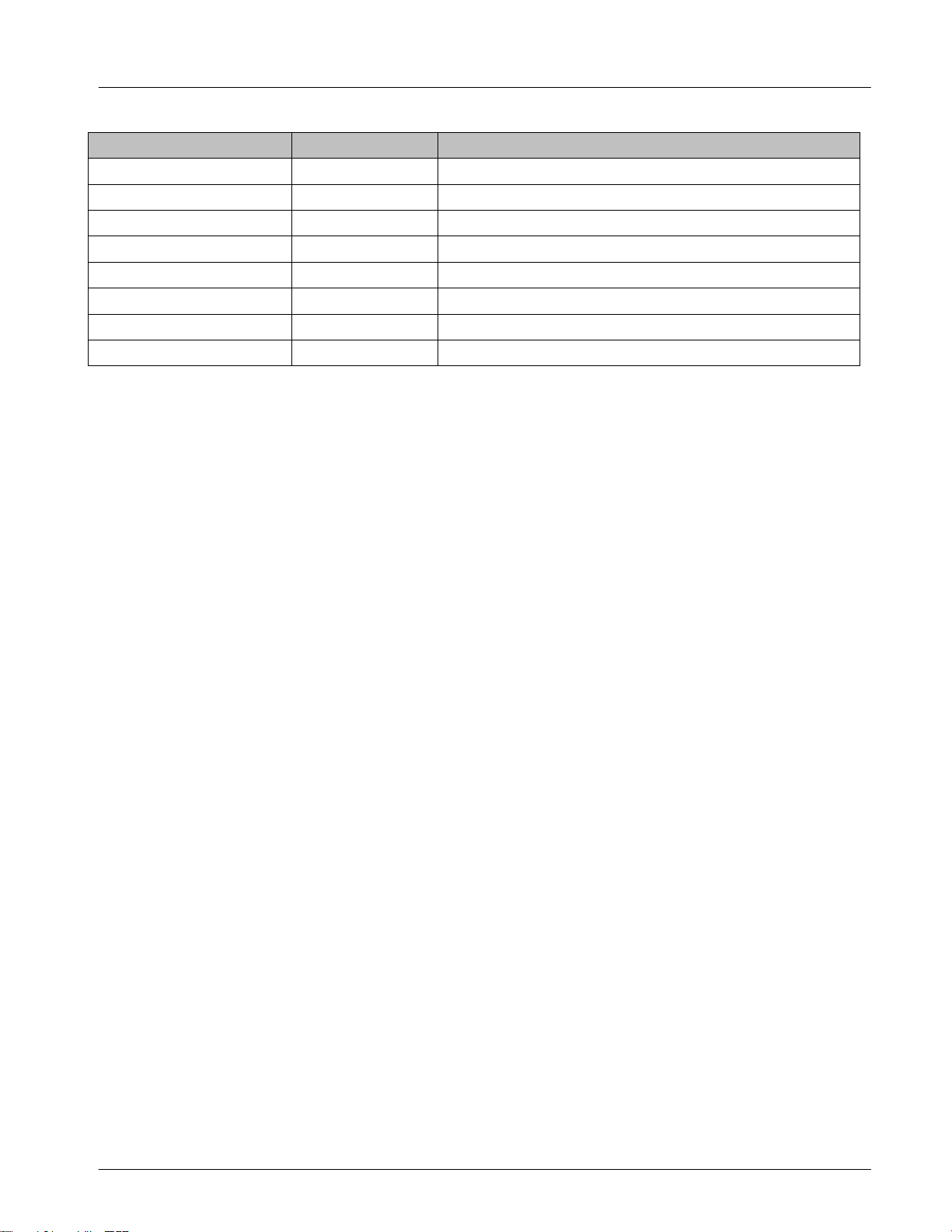
Main Electrical Parts List
Design LOC SEC CODE Description
R117,R304
R108,R306,R307,R308
R309,R313,R314,R315
R316,R500,R531
R310,R411,R509
R418
R514
R412,R413,R414,R416
R417
R300,R305,R318,R319
R320,R322,R332,R410
R524
R511
R512
R517
R336,R523,R527,R528
R612
R521,R522
R335
R415
R301,R609
R407
R201
R311,R312
R611
R405
R409
R408
R406
R400
R530
R105
R110
R112,R113,R600,R601
R603,R604,R605,R606
R607,R608,R615,R616
2007-000140
2007-000141
2007-000141
2007-000141
2007-000148
2007-000149
2007-000155
2007-000157
2007-000157
2007-000162
2007-000162
2007-000162
2007-000165
2007-000168
2007-000170
2007-000172
2007-000242
2007-001292
2007-001298
2007-001339
2007-003001
2007-007107
2007-007132
2007-007139
2007-007193
2007-007334
2007-007468
2007-007480
2007-007573
2007-007698
2007-007798
2007-008043
2007-008044
2007-008045
2007-008045
2007-008045
R-CHIP
R-CHIP
R-CHIP
R-CHIP
R-CHIP
R-CHIP
R-CHIP
R-CHIP
R-CHIP
R-CHIP
R-CHIP
R-CHIP
R-CHIP
R-CHIP
R-CHIP
R-CHIP
R-CHIP
R-CHIP
R-CHIP
R-CHIP
R-CHIP
R-CHIP
R-CHIP
R-CHIP
R-CHIP
R-CHIP
R-CHIP
R-CHIP
R-CHIP
R-CHIP
R-CHIP
R-CHIP
R-CHIP
R-CHIP
R-CHIP
R-CHIP
5-2
SAMSUNG Proprietary-Contents may change without notice
This Document can not be used without Samsung's authorization

Design LOC SEC CODE Description
R617,R618,R619,R620
R106
R107
R515,R529
R302
R520
R109
R111
R325
R507,R508
R403
R404
R116,R123
R200
C126,C189,C226,C230
C231,C436
C102,C108,C217
C179,C215,C219,C238
C326
C321
C434,C435,C513,C614
C107,C110,C112,C233
C501
C130,C133,C329
C430
C117
C109,C113,C119,C127
C128,C129,C145,C146
C148,C454,C457,C458
C459
C213
C122,C330,C431
C114
C180
C406,C407
C242
2007-008045
2007-008046
2007-008049
2007-008055
2007-008298
2007-008516
2007-008588
2007-008647
2007-008766
2007-008774
2007-008806
2007-008812
2007-009766
2007-009794
2203-000233
2203-000233
2203-000254
2203-000278
2203-000311
2203-000386
2203-000425
2203-000438
2203-000438
2203-000489
2203-000585
2203-000679
2203-000812
2203-000812
2203-000812
2203-000812
2203-000940
2203-000995
2203-001017
2203-001383
2203-001405
2203-002668
Main Electrical Parts List
R-CHIP
R-CHIP
R-CHIP
R-CHIP
R-CHIP
R-CHIP
R-CHIP
R-CHIP
R-CHIP
R-CHIP
R-CHIP
R-CHIP
R-CHIP
R-CHIP
C-CERAMIC,CHIP
C-CERAMIC,CHIP
C-CERAMIC,CHIP
C-CERAMIC,CHIP
C-CERAMIC,CHIP
C-CERAMIC,CHIP
C-CERAMIC,CHIP
C-CERAMIC,CHIP
C-CERAMIC,CHIP
C-CERAMIC,CHIP
C-CERAMIC,CHIP
C-CERAMIC,CHIP
C-CERAMIC,CHIP
C-CERAMIC,CHIP
C-CERAMIC,CHIP
C-CERAMIC,CHIP
C-CERAMIC,CHIP
C-CERAMIC,CHIP
C-CERAMIC,CHIP
C-CERAMIC,CHIP
C-CERAMIC,CHIP
C-CERAMIC,CHIP
5-3
SAMSUNG Proprietary-Contents may change without notice
This Document can not be used without Samsung's authorization

Main Electrical Parts List
Design LOC SEC CODE Description
C111,C201,C203,C205
C210,C220,C221,C223
C224,C300,C303,C304
C305,C310,C312,C316
C324,C325,C327,C328
C437,C443,C447,C448
C606,C607,C608,C610
C144
C241
C147,C232
C240
C208,C209
C234
C139,C142
C162,C163,C164,C322
C172,C173
C138,C140,C151,C161
C239
C158,C165,C186
C150
C170
C229
C323
C204,C207,C212,C235
C314,C315,C462,C506
C507,C611
C118,C120
C168,C176
C612
C404
C313,C410,C414,C415
C416,C417,C419,C423
C425,C428,C429,C432
C445,C449,C450,C451
C452,C461,C605
C157,C160,C166,C169
2203-002709
2203-002709
2203-002709
2203-002709
2203-002709
2203-002709
2203-002709
2203-005050
2203-005052
2203-005281
2203-005288
2203-005393
2203-005450
2203-005552
2203-005682
2203-005725
2203-005732
2203-005734
2203-005736
2203-005792
2203-005806
2203-005968
2203-006047
2203-006048
2203-006048
2203-006048
2203-006187
2203-006194
2203-006201
2203-006260
2203-006399
2203-006399
2203-006399
2203-006399
2203-006399
2203-006423
C-CERAMIC,CHIP
C-CERAMIC,CHIP
C-CERAMIC,CHIP
C-CERAMIC,CHIP
C-CERAMIC,CHIP
C-CERAMIC,CHIP
C-CERAMIC,CHIP
C-CERAMIC,CHIP
C-CERAMIC,CHIP
C-CERAMIC,CHIP
C-CERAMIC,CHIP
C-CERAMIC,CHIP
C-CERAMIC,CHIP
C-CERAMIC,CHIP
C-CERAMIC,CHIP
C-CERAMIC,CHIP
C-CERAMIC,CHIP
C-CERAMIC,CHIP
C-CERAMIC,CHIP
C-CERAMIC,CHIP
C-CERAMIC,CHIP
C-CERAMIC,CHIP
C-CERAMIC,CHIP
C-CERAMIC,CHIP
C-CERAMIC,CHIP
C-CERAMIC,CHIP
C-CERAMIC,CHIP
C-CERAMIC,CHIP
C-CERAMIC,CHIP
C-CERAMIC,CHIP
C-CERAMIC,CHIP
C-CERAMIC,CHIP
C-CERAMIC,CHIP
C-CERAMIC,CHIP
C-CERAMIC,CHIP
C-CERAMIC,CHIP
5-4
SAMSUNG Proprietary-Contents may change without notice
This Document can not be used without Samsung's authorization
Design LOC SEC CODE Description
C175,C178,C182,C184
C187
C216,C218,C227,C228
C236,C301,C302,C306
C318,C319,C408,C409
C442,C446,C503,C508
C600,C602,C603,C604
C131,C135
C134,C400,C401,C402
C403,C438,C439,C440
C441,C520
C200,C202,C211
C308,C309
C433
C517
C500
C206,C222,C237,C411
C412,C413,C418,C422
C424,C426,C427,C453
C515,C516
C116,C455,C609
C185
C307,C311,C505
C519
C456
BAT400
L126,L133
L124
L120
L127
L105,L122
R333
L113
L132
C225,L131,L212
L117,L130
2203-006423
2203-006423
2203-006562
2203-006562
2203-006562
2203-006562
2203-006562
2203-006707
2203-006824
2203-006824
2203-006824
2203-006838
2203-006839
2203-006841
2203-006978
2203-007240
2203-007271
2203-007271
2203-007271
2203-007271
2203-007279
2203-007317
2203-007474
2203-007634
2203-007775
2409-001172
2703-001178
2703-001729
2703-001737
2703-001750
2703-001786
2703-001990
2703-002170
2703-002176
2703-002208
2703-002281
Main Electrical Parts List
C-CERAMIC,CHIP
C-CERAMIC,CHIP
C-CERAMIC,CHIP
C-CERAMIC,CHIP
C-CERAMIC,CHIP
C-CERAMIC,CHIP
C-CERAMIC,CHIP
C-CERAMIC,CHIP
C-CERAMIC,CHIP
C-CERAMIC,CHIP
C-CERAMIC,CHIP
C-CERAMIC,CHIP
C-CERAMIC,CHIP
C-CERAMIC,CHIP
C-CERAMIC,CHIP
C-CERAMIC,CHIP
C-CERAMIC,CHIP
C-CERAMIC,CHIP
C-CERAMIC,CHIP
C-CERAMIC,CHIP
C-CERAMIC,CHIP
C-CERAMIC,CHIP
C-CERAMIC,CHIP
C-CERAMIC,CHIP
C-CERAMIC,CHIP
CAPACITOR
INDUCTOR-SMD
INDUCTOR-SMD
INDUCTOR-SMD
INDUCTOR-SMD
INDUCTOR-SMD
INDUCTOR-SMD
INDUCTOR-SMD
INDUCTOR-SMD
INDUCTOR-SMD
INDUCTOR-SMD
5-5
SAMSUNG Proprietary-Contents may change without notice
This Document can not be used without Samsung's authorization

Main Electrical Parts List
Design LOC SEC CODE Description
L509
L110,L207
L128,L129
L107
L115
L211
L503
L400,L401,L402,L403
L118,L121
OSC400
OSC200
OSC100
F600,F601,F602,F603
F604,F605,F606,F607
F608,F609
F103
F104
F102
F101
DUF101
DUF100
L206
L202,L203
L104
L504,L505,L506,L507
L204
SW600,SW601,SW602
RFS100
CN603
HEA601
BTC400
HEA500
L108,L109,L200,L205
MOT500,MOT501
IFC500
F200
2703-002308
2703-002314
2703-002365
2703-002367
2703-002958
2703-003004
2703-003485
2703-003686
2703-003915
2801-004909
2801-005045
2809-001366
2901-001424
2901-001424
2901-001424
2904-001658
2904-001702
2904-001908
2904-001920
2910-000099
2910-000117
3301-001438
3301-001659
3301-001756
3301-001885
3301-001895
3404-001410
3705-001731
3708-002222
3711-005937
3711-007533
3711-007592
3712-001348
3712-001348
3722-003065
2911-000162
INDUCTOR-SMD
INDUCTOR-SMD
INDUCTOR-SMD
INDUCTOR-SMD
INDUCTOR-SMD
INDUCTOR-SMD
INDUCTOR-SMD
INDUCTOR-SMD
INDUCTOR-SMD
CRYSTAL-UNIT
CRYSTAL-UNIT
OSCILLATOR-VCTCXO
FILTER-EMI SMD
FILTER-EMI SMD
FILTER-EMI SMD
FILTER-SAW
FILTER-SAW
FILTER-SAW
FILTER-SAW
FILTER
FILTER
CORE-FERRITE BEAD
CORE-FERRITE BEAD
CORE-FERRITE BEAD
CORE-FERRITE BEAD
CORE-FERRITE BEAD
SWITCH-TACT
CONNECTOR-COAXIAL
CONNECTOR-FPC/FFC/PIC
CONNECTOR-HEADER
CONNECTOR-HEADER
CONNECTOR-HEADER
CONNECTOR
CONNECTOR
JACK-PHONE
FILTER
5-6
SAMSUNG Proprietary-Contents may change without notice
This Document can not be used without Samsung's authorization
Main Electrical Parts List
Design LOC SEC CODE Description
UME300
L123
L112,L114,L116
HEA401
HEA600
HEA400
F201
F100
Please consult the GSPN website (Samsung Portal) for the most recent version of the product's part list.
1108-000411
2703-003917
2703-004030
3711-007762
3711-005456
3709-001681
1201-003216
2904-001889
MEMORY
INDUCTOR-SMD
INDUCTOR-SMD
CONNECTOR-HEADER
CONNECTOR-HEADER
CONNECTOR-CARD EDGE
IC
FILTER-SAW
5-7
SAMSUNG Proprietary-Contents may change without notice
This Document can not be used without Samsung's authorization
Level
6.
S/W Download
6-1.
Repair
1
6-1-1.
Pre-requsite for S/W Downloading
GT-B7510 Mobile Phone
•
Battery
•
USB cable
•
JIG BOX(GH99-36900A)
•
RF Test Cable(GH39-00985A)
•
JIG Cable(GH39-01339A)
•
Adapter(GH99-38251A)
•
Downloader Program(
•
Binary files
•
PC(Windows XP,
•
The settings for download.
★
7)
Odin Multi Downloader v4.38)
6-1
SAMSUNG Proprietary-Contents may change without notice
This Document can not be used without Samsung's authorization
Level1Repair
6-1-2.
S/W Downloader Program
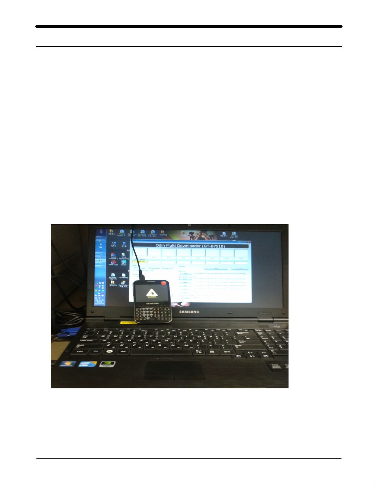
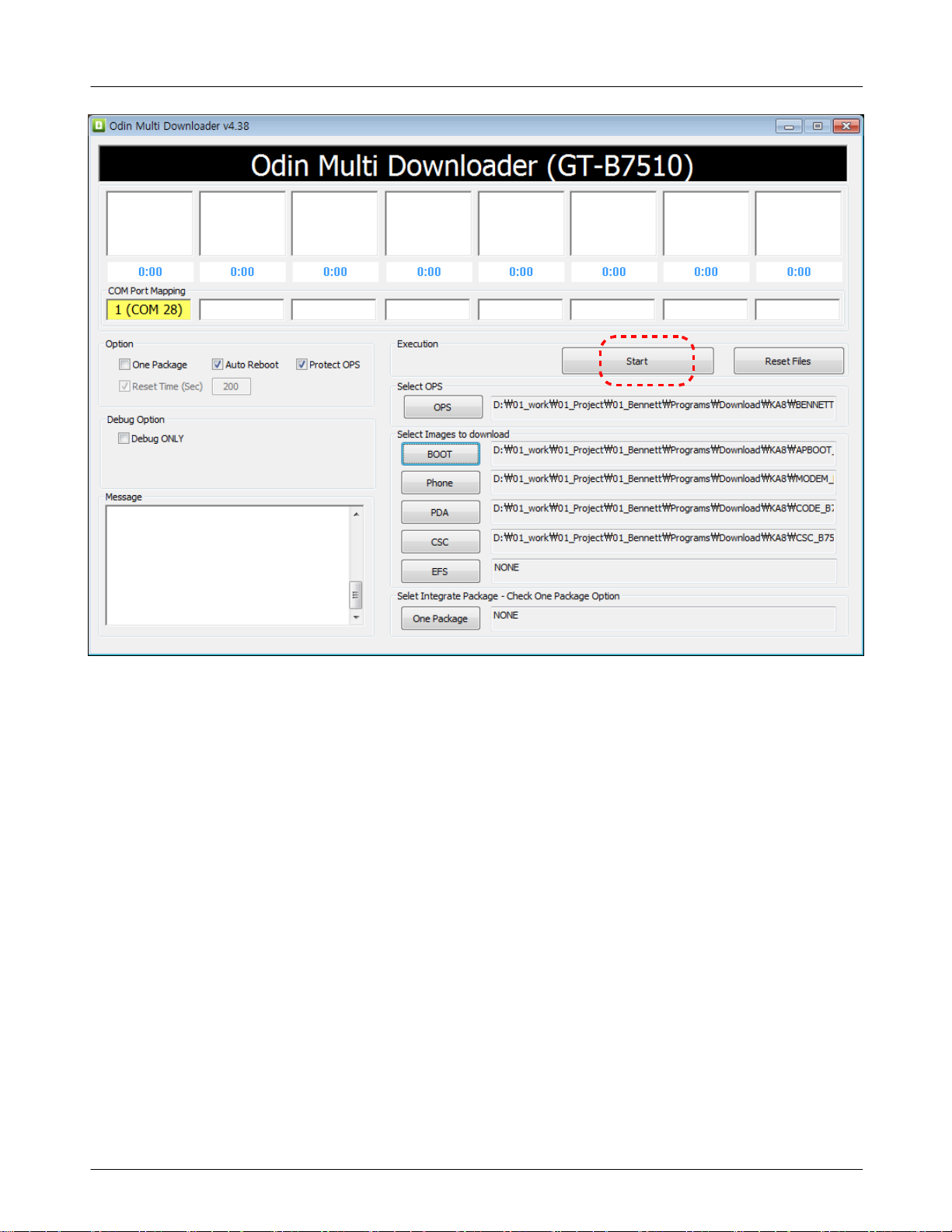
Execute the binary download program,which is"Odin Multi Downloader v4.38".
1.
Load the files of OPS, BOOT, PHONE, PDS, CSC from the folder that you saved
2.
binary files.(CLICK the each Naming Button and select the file)
OPS:OPS file
-
BOOT:APBOOT_...
-
phone:MODEM_...
-
PDA:CODE_...
-
CSC:CSC_...
-
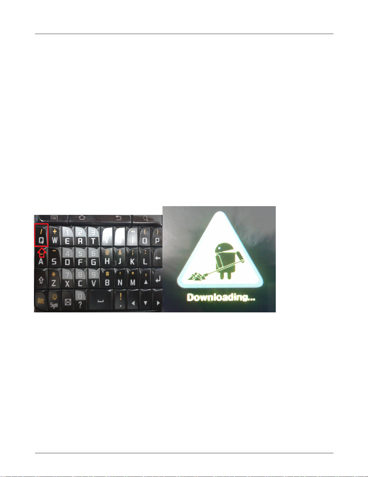
Turn On the Mobile with push'Q' Button to enter the Download mode and check
3.
the Download Logo on LCD
QWERTY Key Pad
<
Click the Start button whenaport is ready
4.
><
SAMSUNG Proprietary-Contents may change without notice
This Document can not be used without Samsung's authorization
Download Logo>
6-2
Level1Repair
After downloading finished successfully, there is
5.
Check the binary version using key streaming,
6.
PASS" message.
a "
"*#1234#".
6-3
SAMSUNG Proprietary-Contents may change without notice
This Document can not be used without Samsung's authorization
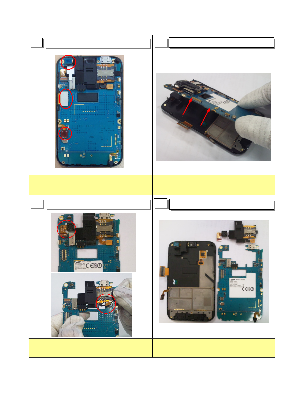
Level
7.
Disassembly and Assembly Instructions
7-1.
Repair
2
7-1-1.
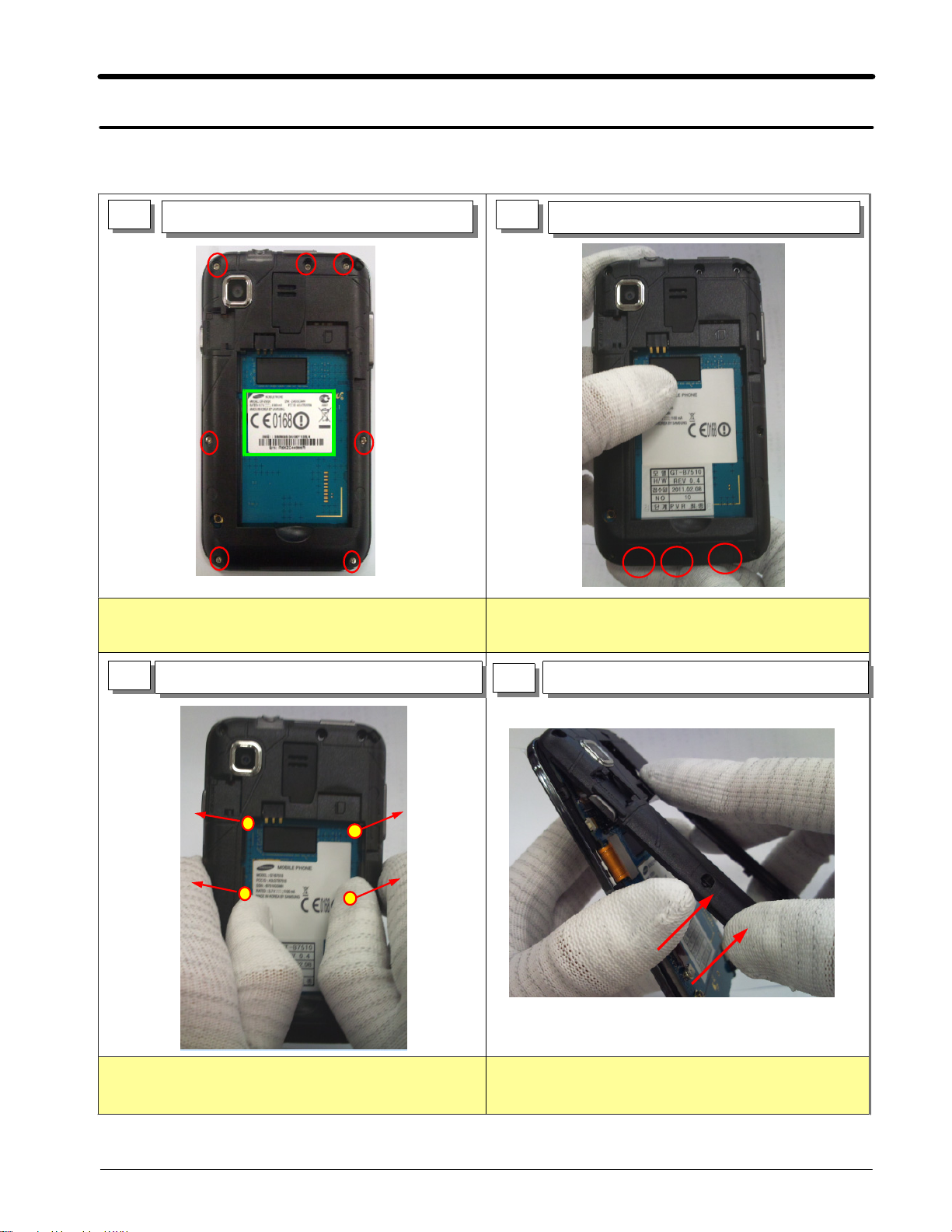
1)
Disassembly
1 2
Be careful not to make scratch and molding damage!
Release Screw7Point at REAR
Disjoint Hook on the bottom of the REAR
Be careful not to make scratch and molding damage!
1)
3
Disjoint hook on the both side of the REAR
Push out REAR to both side.
1)
Disassemble REAR
4
Detach Power Key FPCB and Cammera Key FPCB.
1)
Be careful not to damage to FPCB(Use tweezer!)
2)
7-1
SAMSUNG Proprietary-Contents may change without notice
This Document can not be used without Samsung's authorization
Level2Repair
7.
5
Disassemble FPCB.
6
Disassemble Main PBA from the FRONT Ass'y
Detach Earjack/LCD/Qwerty key FPCB.(3point)
1)
7
Disassemble Module from PBA.
Hold up Main PBA from left.
1)
8
Complete disassembly.
Disassemble Cammera Module from PBA.
1)
Disassemble SPK Module from PBA.
2)
SAMSUNG Proprietary-Contents may change without notice
This Document can not be used without Samsung's authorization
7-2
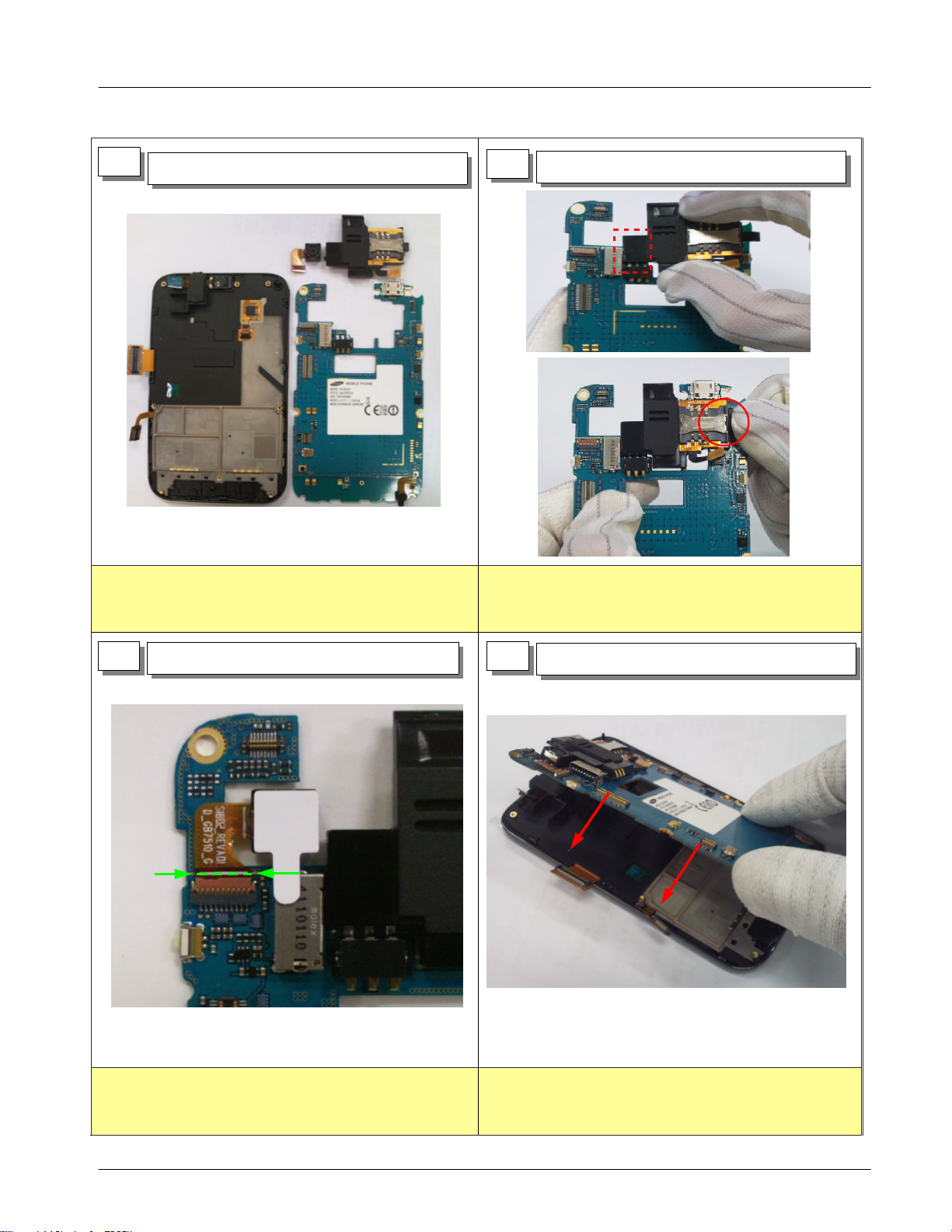
Level2Repair
7.
7-1-1.
1
Assembly
SetaPBA and FRONT Ass'y.
2
Assemble SPK module.
3
Assemble Camera module
Assemble left hook first.
1)
Assemble right hook.
2)
4
Assemble PBA on FRONT Ass'y.
Assemble fiting to silk line
1)
7-3
SAMSUNG Proprietary-Contents may change without notice
This Document can not be used without Samsung's authorization
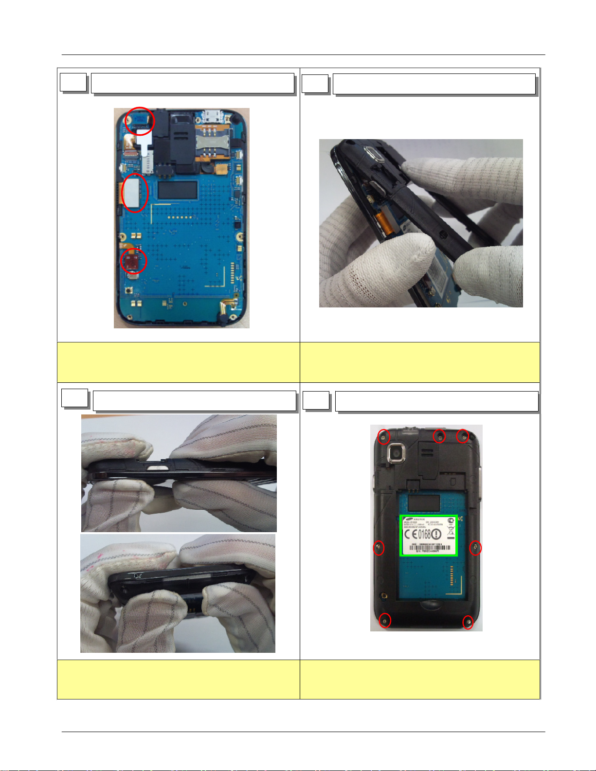
Level2Repair
7.
5
Assemble PBA on FRONT Ass'y.
6
Assemble FRONT Ass'y on REAR.
Assemble Earjack/LCD/Qwerty key FPCB.(3point).
1)
Be careful not to damage to FPCB.
2)
7
Assemble FRONT Ass'y on REAR.
Assemble matching location from earjack of rear
1)
upper
8
Drive Screws at6points
Be careful not to make scratch and molding damage!
1)
SAMSUNG Proprietary-Contents may change without notice
This Document can not be used without Samsung's authorization
Drive Screws at6points with torque
1)
1.1 +/- 0.1
Kgf/
㎠
7-4
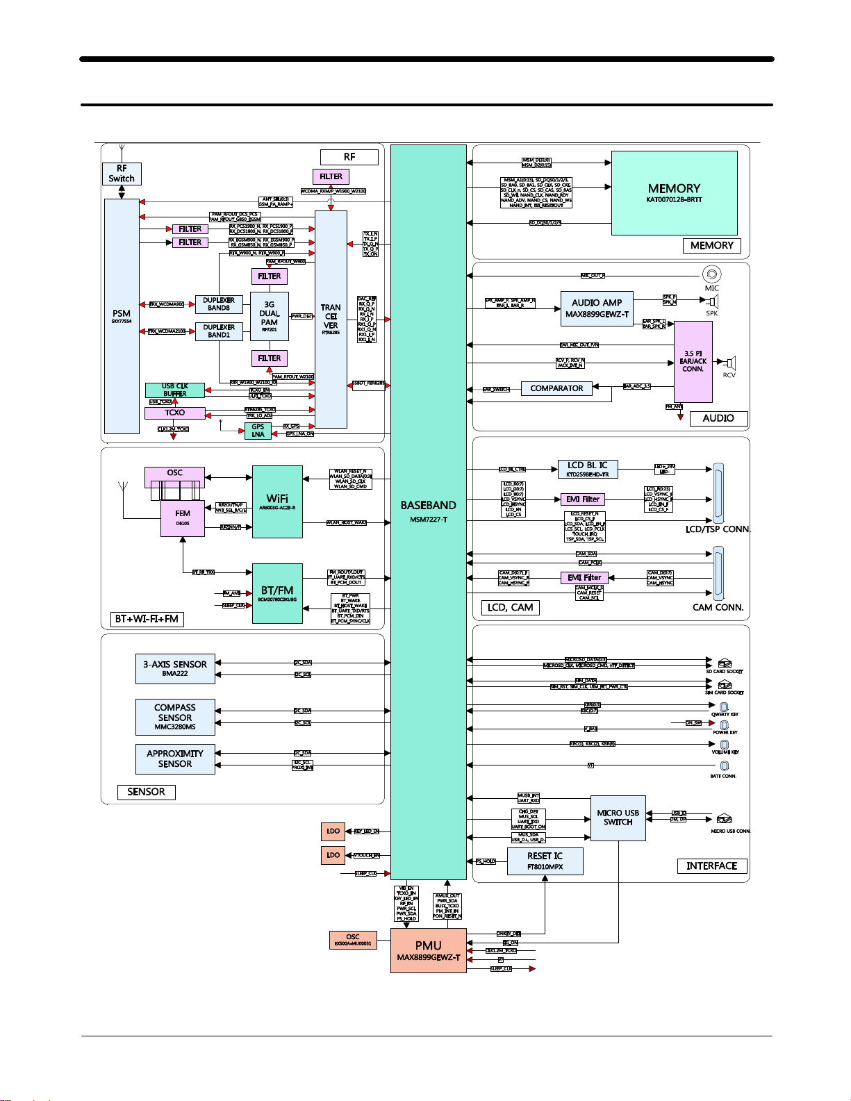
Level
8.
Block Diagram
8-1.
Repair
3
8-1
SAMSUNG Proprietary-Contents may change without notice
This Document can not be used without Samsung's authorization
 Loading...