

Samsung B7330B Service Manual
GSM TELEPHONE
GT-B7330B
GSM TELEPHONE
CONTENTS
Safety Precautions
1.
Specification
2.
Product Function
3.
Exploded View and Parts list
4.
MAIN Electrical Parts List
5.
Level1Repair
6.
S/W Download
6-1.
Level2Repair
7.
Disassembly and Assembly Instructions
7-1.
Calibration
7-2.
IMEI/ESN Writing
7-3.
Level3Repair
8.
Block Diagram
8-1.
PCB Diagram
8-2.
Troubleshooting
8-3.
Service Schematics
8-4.
Reference data
9.

Safety Precautions
1.
Repair Precaution
1-1.
Repair in Shield Box, during detailed tuning.
―
Take specially care of tuning or test, because the specification of cellular phone is sensitive for
surrounding interference(RF noise).
Be careful to useakind of magnetic object or tool, because performance of parts is damaged by
―
the influence of magnetic force.
Surely useastandard screwdriver when you disassemble this product, otherwise screw will be
―
worn away.
Useathicken twisted wire when you measure level.
―
thicken twisted wire has low resistance, therefore error of measurement is few.
A
Repair after separate Test Pack and Set because for short danger(for example an overcurrent
―
and furious flames of parts etc) when you repair board in condition of connecting Test Pack and
tuning on.
Take specially care of soldering, because Land of PCB is small and weak in heat.
―
Surely tune on/off while using AC power plug, becausearepair of battery charger is dangerous
―
when tuning ON/OFF PBA and Connector after disassembling charger.
Don't use as you pleases after change other material than replacement registered on SEC System.
―
Otherwise engineer in charge isn't charged with problem that you don't keep this rules.
1-1
SAMSUNG Proprietary-Contents may change without notice
This Document can not be used without Samsung's authorization

Safety Precautions
ESD(Electrostatically Sensitive Devices) Precaution
1-2.
Several semiconductor may be damaged easily by static electricity. Such parts are called by ESD
Electrostatically Sensitive Devices), for example IC,BGA chip etc. Read Precaution below.
(
You can prevent from ESD damage by static electricity.
Remove static electricity remained your body before you touch semiconductor or parts with
―
semiconductor. There are ways that you touch an earthed place or wear static electricity prevention
string on wrist.
Use earthed soldering steel when you connect or disconnect ESD.
―
Use soldering removing tool to break static electricity.Otherwise ESD will be damaged by static
―
electricity.
Don't unpack until you set up ESD on product. Because most of ESD are packed by box and
―
aluminum plate to have conductive power,they are prevented from static electricity.
You must maintain electric contact between ESD and place due to be set up until ESD is
―
connected completely to the proper place oracircuit board.
1-2
SAMSUNG Proprietary-Contents may change without notice
This Document can not be used without Samsung's authorization
Specification
2.
GSM General Specification
2-1.
GSM 850 EGSM 900 DCS1800 PCS1900
Freq. Band[MHz]
Uplink/Downlink
ARFCN range 128~25
Tx/Rx spacing 45MHz 45MHz 95MHz 80MHz 45MHz 130MHz
Mod. Bit rate/
Bit Period
Time Slot
Period/Frame
Period
824~849
869~894
270.833kbps
3.692us
576.9us
4.615ms
880~915
925~960
0~124 &
975~1023
270.833kbps
3.692us
576.9us
4.615ms
1710~1785
1805~1880
512~885 512~810
270.833kbps
3.692us
576.9us
4.615ms
1850~1910
1930~1990
270.833kbps
3.692us
576.9us
4.615ms
W-CDMA
900
880-915
925-960
UL:2712-2863
DL: 2937
-3088
3.84Mcps
Frame length:
10ms
Slot length :
0.667ms
W-CDMA
2100
1920~1980
2110~2170
UL:9612~9888
DL:10562~
10838
3.84Mcps
Frame length:
10ms
Slot length :
0.667ms
Modulation 0.3GMSK 0.3GMSK 0.3GMSK 0.3GMSK
MS Power
Power Class
Sensitivity -102dBm -102dBm -100dBm -100dBm -106.7dBm -106.7dBm
TDMAMux8888 - -
Cell Radius 35Km 35Km 2Km 2Km 2Km 2Km
33dBm
~5dBm
4
(max
+33dBm)
33dBm
~5dBm
4
(max
+33dBm)
30dBm
~0dBm
1
(max
+30dBm)
30dBm
~0dBm
1
(max
+30dBm)
QPSK
HQPSK
24dBm ~ -
50dBm
3
(max +24dBm)3(max +24dBm)
QPSK
HQPSK
24dBm ~ -
50dBm
2-1
SAMSUNG Proprietary-Contents may change without notice
This Document can not be used without Samsung's authorization
GSM Tx Power Class
2-2.
Specification
TX Power
control level
533±2
631±2
729±2
827±2
925±2
10 23±2
11 21±2
GSM850
GSM900
dBm
dBm
dBm
dBm
dBm
dBm
dBm
TX Power
control level
030±3
128±3
226±3
324±3
422±3
520±3
618±3
DCS1800
dBm
dBm
dBm
dBm
dBm
dBm
dBm
TX Power
PCS1900
control level
030±3
128±3
226±3
324±3
422±3
520±3
618±3
dBm
dBm
dBm
dBm
dBm
dBm
dBm
12 19±2
13 17±2
14 15±2
15 13±2
16 11±3
17 9±3
18 7±3
19 5±3
dBm
dBm
dBm
dBm
dBm
dBm
dBm
dBm
716±3
814±3
912±4
10 10±4
11 8±4
12 6±4
13 4±4
14 2±5
15 0±5
dBm
dBm
dBm
dBm
dBm
dBm
dBm
dBm
dBm
716±3
814±3
912±4
10 10±4
11 8±4
12 6±4
13 4±4
14 2±5
15 0±5
dBm
dBm
dBm
dBm
dBm
dBm
dBm
dBm
dBm
2-2
SAMSUNG Proprietary-Contents may change without notice
This Document can not be used without Samsung's authorization

Product Function
3.
Main Function
HSDPA/HSUPA/ UMTS, EDGE, GPRS
-
MP3
-
BT
-
Video Sharing/Streaming
-
USB
-
WAP2.0, JAVA, MPEG4
-
MIDP
-
Auto Time Setting,
-
MMS/SMS
-
Weight:
-
Camera:
-
LCD
-
Size:
-
GPRS/EDGE:class
-
Battery:
-
Memory:
-
Band: GSM
-
BB: Qualcomm MSM7225
-
RF: Qualcomm RTR6285
-
WLAN
-
A-GPS
-
/40
2.1 +
2.0
2.0 /
: 2.62"
114.9
Poly Melody
EDR
CLDC
109g
Mega Pixel, CMOS
3.2
TFT(LCD)
x59x10.8 mm
mAH
1500
MB DDR
256
850/900/1800/1900,
802.11
b/g
1.1
12
+512
MB ROM
FDD1, FDD8
3-1
SAMSUNG Proprietary-Contents may change without notice
This Document can not be used without Samsung's authorization
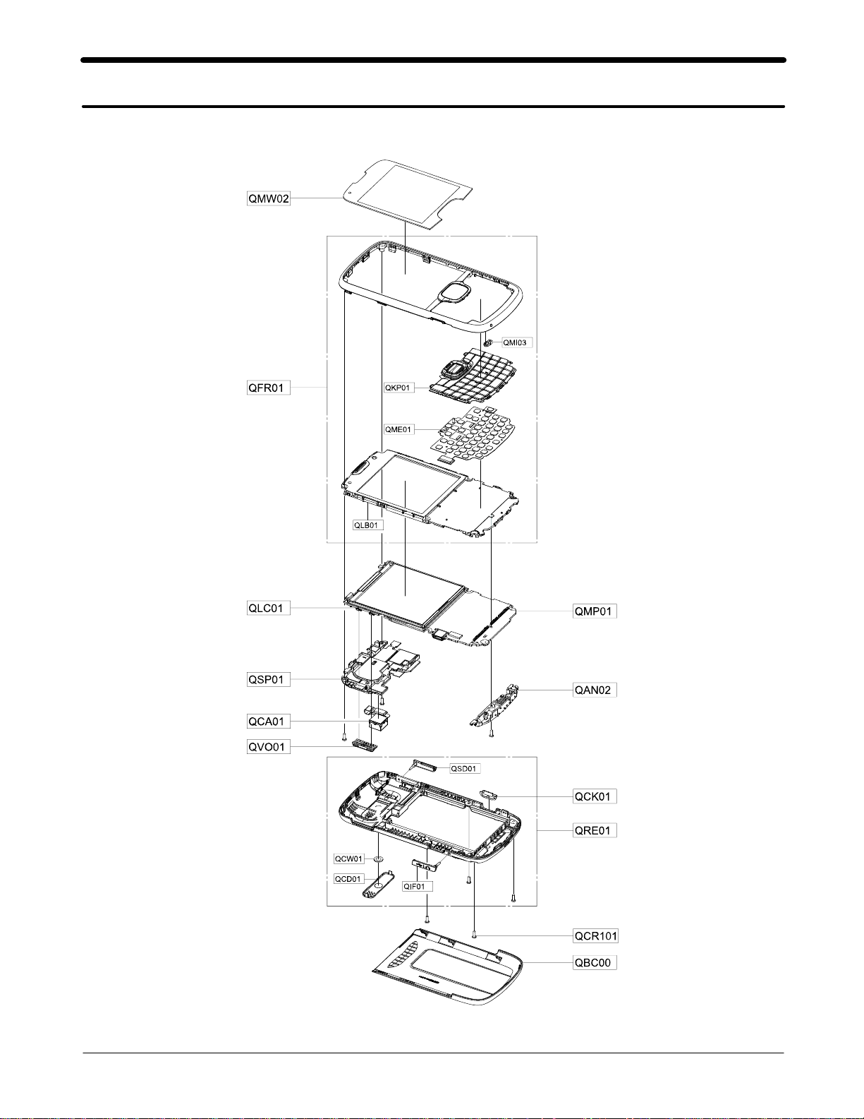
Exploded View and Parts List
4.
Cellular phone Exploded View
4-1.
4-1
SAMSUNG Proprietary-Contents may change without notice
This Document can not be used without Samsung's authorization
Exploded View and Parts List
Cellular phone Parts list
4-2.
Design LOC Discription SEC CODE
QCR101 SCREW-MACHINE
QLC01 LCD-L5F30977 GH07-01446A
QAN02 INTENNA-MAIN(GT-B7330B) GH42-02414A
QSP01 MODULE-SPK+ENCLOSURE(GT-B7330) GH59-07783A
QMW02 PCT WINDOW-MAIN_CANADA GH72-58030A
QMP01 A/S ASSY-PBA MAIN(CNDA)GT-B7330B GH82-04763A
QCA01 ASSY CAMERA-CAM MOD ASSY,GT-B7330(3M) GH96-03957A
QVO01 ASSY KEY-VOL GH98-13565A
QCK01 ASSY KEY-CAM GH98-13566A
QBC00 ASSY COVER-BATT GH98-14193A
QFR01 ASSY CASE-FRONT GH98-16282A
QME01 KEY FPCB-GT-B7330 GH59-07785A
QMI03 RMO RUBBER-MIC GH73-13228A
QLB01 ASSY BRACKET-LCD GH98-16097A
QKP01 ASSY KEYPAD-(BLK/BMC) GH98-16491A
QRE01 ASSY CASE-REAR GH98-13563A
QIF01 PMO COVER-IF GH72-54474A
QSD01 PMO COVER-SD GH72-54475A
QCW01 PCT WINDOW-CAM GH72-54483A
QCD01 ASSY DECO-CAM GH98-14192A
6001-002005
4-2
SAMSUNG Proprietary-Contents may change without notice
This Document can not be used without Samsung's authorization
MAIN Electrical Parts List
5.
SEC CODE Design LOC Discription
0403-001741
0404-001245
0406-001167
0406-001167
0406-001267
0406-001267
0406-001267
0406-001267
0406-001267
0406-001267
0406-001267
0406-001267
0406-001281
0406-001281
0406-001369
0406-001375
0406-001375
0407-001002
0407-001002
0504-000168
0505-002088
0601-001905
0801-003139
0801-003200
0801-003265
1001-001488
1001-001580
1001-001593
1108-000262
1201-002856
1201-002864
1201-002887
1201-002888
1201-002961
1203-003924
1203-004596
1203-004776
1203-004792
1203-004798
1203-004802
1203-004818
1203-004945
1203-005092
ZD603 DIODE-ZENER
D700 DIODE-SCHOTTKY
ZD507 DIODE-TVS
ZD508 DIODE-TVS
D600 DIODE-TVS
ZD500 DIODE-TVS
ZD501 DIODE-TVS
ZD504 DIODE-TVS
ZD505 DIODE-TVS
ZD506 DIODE-TVS
ZD509 DIODE-TVS
ZD510 DIODE-TVS
ZD502 DIODE-TVS
ZD503 DIODE-TVS
ZD602 DIODE-TVS
ZD600 DIODE-TVS
ZD601 DIODE-TVS
D400 DIODE-ARRAY
D500 DIODE-ARRAY
TR401 TR-DIGITAL
Q600 FET-SILICON
LED500 LED
U203 IC-CMOS LOGIC
U301 IC-CMOS LOGIC
U300 IC-CMOS LOGIC
U501 IC-ANALOG SWITCH
U600 IC-ANALOG MULTIPLEX
U601 IC-ANALOG SWITCH
UME300 IC-MCP
U202 IC-RF AMP
U500 IC-AUDIO AMP
PAM200 IC-POWER AMP
PAM202 IC-POWER AMP
PAM100 IC-POWER AMP
U402 IC-VOL. DETECTOR
U701 IC-MULTI REG.
U704 IC-POSI.FIXED REG.
U705 IC-POSI.FIXED REG.
U502 IC-SWITCH VOL. REG.
U201 IC-POSI.FIXED REG.
U703 IC-POSI.FIXED REG.
U702 IC-MULTI REG.
U401 IC-POWER SUPERVISOR
5-1
SAMSUNG Proprietary-Contents may change without notice
This Document can not be used without Samsung's authorization

Main Electrical Parts List
SEC CODE Design LOC Discription
1203-005225
1203-005554
1203-005689
1203-005916
1204-002746
1205-003297
1205-003790
1404-001221
2007-000138
2007-000141
2007-000148
2007-000148
2007-000171
2007-000174
2007-001217
2007-007008
2007-007014
2007-007014
2007-007190
2007-007190
2007-007309
2007-007310
2007-007317
2007-007317
2007-007318
2007-007468
2007-007798
2007-007798
2007-008045
2007-008045
2007-008045
2007-008045
2007-008045
2007-008045
2007-008046
2007-008046
2007-008049
2007-008055
2007-008055
2007-008055
2007-008055
2007-008055
2007-008055
U706 IC-MULTI REG.
U405 IC-VOL. DETECTOR
U602 IC-BATTERY
U700 IC-BACKLIGHT DRIVER
U200 IC-TUNER
U100 IC-TRANSCEIVER
UCP300 IC-MODEM
TH400 THERMISTOR-NTC
R321 R-CHIP
R103 R-CHIP
R208 R-CHIP
R420 R-CHIP
R118 R-CHIP
R505 R-CHIP
R504 R-CHIP
R503 R-CHIP
R402 R-CHIP
R406 R-CHIP
R500 R-CHIP
R501 R-CHIP
R108 R-CHIP
R605 R-CHIP
R311 R-CHIP
R312 R-CHIP
R603 R-CHIP
R409 R-CHIP
R701 R-CHIP
R702 R-CHIP
R111 R-CHIP
R207 R-CHIP
R324 R-CHIP
R327 R-CHIP
R502 R-CHIP
R610 R-CHIP
R106 R-CHIP
R107 R-CHIP
R329 R-CHIP
R300 R-CHIP
R315 R-CHIP
R328 R-CHIP
R400 R-CHIP
R401 R-CHIP
R403 R-CHIP
5-2
SAMSUNG Proprietary-Contents may change without notice
This Document can not be used without Samsung's authorization

Main Electrical Parts List
SEC CODE Design LOC Discription
2007-008055
2007-008055
2007-008055
2007-008211
2007-008263
2007-008263
2007-008419
2007-008419
2007-008419
2007-008419
2007-008420
2007-008478
2007-008483
2007-008486
2007-008516
2007-008516
2007-008516
2007-008516
2007-008531
2007-008542
2007-008544
2007-008581
2007-008581
2007-008766
2007-008774
2007-008774
2007-008780
2007-008780
2007-008806
2007-008806
2007-008808
2007-008809
2007-008809
2007-008816
2007-009115
2007-009115
2007-009115
2007-009170
2007-009171
2007-009171
2007-009171
2007-009212
2203-000233
R506 R-CHIP
R609 R-CHIP
R611 R-CHIP
R101 R-CHIP
R410 R-CHIP
R604 R-CHIP
R114 R-CHIP
R115 R-CHIP
R116 R-CHIP
R117 R-CHIP
R330 R-CHIP
R608 R-CHIP
R210 R-CHIP
R414 R-CHIP
R205 R-CHIP
R316 R-CHIP
R318 R-CHIP
R320 R-CHIP
R206 R-CHIP
R109 R-CHIP
R606 R-CHIP
R104 R-CHIP
R105 R-CHIP
R323 R-CHIP
R601 R-CHIP
R602 R-CHIP
R110 R-CHIP
R112 R-CHIP
R100 R-CHIP
R408 R-CHIP
R202 R-CHIP
R301 R-CHIP
R309 R-CHIP
R317 R-CHIP
R200 R-CHIP
R201 R-CHIP
R204 R-CHIP
R415 R-CHIP
R302 R-CHIP
R507 R-CHIP
R508 R-CHIP
R113 R-CHIP
C114 C-CER,CHIP
5-3
SAMSUNG Proprietary-Contents may change without notice
This Document can not be used without Samsung's authorization

Main Electrical Parts List
SEC CODE Design LOC Discription
2203-000233
2203-000233
2203-000233
2203-000233
2203-000233
2203-000233
2203-000233
2203-000233
2203-000233
2203-000278
2203-000386
2203-000386
2203-000386
2203-000386
2203-000438
2203-000627
2203-000627
2203-000812
2203-000812
2203-000812
2203-000812
2203-000812
2203-000812
2203-000812
2203-000812
2203-000854
2203-001153
2203-001153
2203-001239
2203-001259
2203-001405
2203-001405
2203-001437
2203-002668
2203-002668
2203-002677
2203-005281
2203-005281
2203-005288
2203-005288
2203-005395
2203-005395
2203-005395
C202 C-CER,CHIP
C204 C-CER,CHIP
C209 C-CER,CHIP
C224 C-CER,CHIP
C225 C-CER,CHIP
C243 C-CER,CHIP
C244 C-CER,CHIP
C249 C-CER,CHIP
C425 C-CER,CHIP
C246 C-CER,CHIP
C327 C-CER,CHIP
C515 C-CER,CHIP
C709 C-CER,CHIP
C710 C-CER,CHIP
C200 C-CER,CHIP
C423 C-CER,CHIP
C424 C-CER,CHIP
C102 C-CER,CHIP
C501 C-CER,CHIP
C502 C-CER,CHIP
C504 C-CER,CHIP
C505 C-CER,CHIP
C512 C-CER,CHIP
C513 C-CER,CHIP
C516 C-CER,CHIP
C105 C-CER,CHIP
C511 C-CER,CHIP
C607 C-CER,CHIP
C606 C-CER,CHIP
C101 C-CER,CHIP
C506 C-CER,CHIP
C507 C-CER,CHIP
C100 C-CER,CHIP
C205 C-CER,CHIP
C250 C-CER,CHIP
C166 C-CER,CHIP
C138 C-CER,CHIP
C141 C-CER,CHIP
C157 C-CER,CHIP
C226 C-CER,CHIP
C108 C-CER,CHIP
C109 C-CER,CHIP
C165 C-CER,CHIP
5-4
SAMSUNG Proprietary-Contents may change without notice
This Document can not be used without Samsung's authorization

Main Electrical Parts List
SEC CODE Design LOC Discription
2203-005444
2203-005444
2203-005682
2203-005682
2203-005682
2203-005682
2203-005682
2203-005682
2203-005682
2203-005725
2203-005725
2203-005725
2203-005725
2203-005725
2203-005725
2203-005725
2203-005725
2203-005725
2203-005725
2203-005725
2203-005731
2203-005732
2203-005732
2203-005736
2203-005736
2203-005736
2203-005736
2203-005736
2203-005736
2203-005736
2203-005736
2203-005736
2203-005736
2203-005736
2203-005736
2203-005736
2203-005736
2203-005806
2203-005806
2203-005806
2203-005806
2203-005806
2203-005806
C203 C-CER,CHIP
C207 C-CER,CHIP
C139 C-CER,CHIP
C145 C-CER,CHIP
C332 C-CER,CHIP
C432 C-CER,CHIP
C601 C-CER,CHIP
C603 C-CER,CHIP
C605 C-CER,CHIP
C115 C-CER,CHIP
C123 C-CER,CHIP
C128 C-CER,CHIP
C129 C-CER,CHIP
C130 C-CER,CHIP
C131 C-CER,CHIP
C132 C-CER,CHIP
C151 C-CER,CHIP
C158 C-CER,CHIP
C160 C-CER,CHIP
C162 C-CER,CHIP
C433 C-CER,CHIP
C110 C-CER,CHIP
C112 C-CER,CHIP
C111 C-CER,CHIP
C117 C-CER,CHIP
C119 C-CER,CHIP
C120 C-CER,CHIP
C121 C-CER,CHIP
C122 C-CER,CHIP
C127 C-CER,CHIP
C148 C-CER,CHIP
C152 C-CER,CHIP
C155 C-CER,CHIP
C159 C-CER,CHIP
C206 C-CER,CHIP
C228 C-CER,CHIP
C229 C-CER,CHIP
C126 C-CER,CHIP
C142 C-CER,CHIP
C146 C-CER,CHIP
C149 C-CER,CHIP
C212 C-CER,CHIP
C419 C-CER,CHIP
5-5
SAMSUNG Proprietary-Contents may change without notice
This Document can not be used without Samsung's authorization

Main Electrical Parts List
SEC CODE Design LOC Discription
2203-005806
2203-006048
2203-006048
2203-006048
2203-006048
2203-006048
2203-006194
2203-006194
2203-006194
2203-006361
2203-006399
2203-006423
2203-006423
2203-006462
2203-006562
2203-006562
2203-006562
2203-006562
2203-006562
2203-006562
2203-006562
2203-006562
2203-006562
2203-006562
2203-006562
2203-006562
2203-006562
2203-006562
2203-006562
2203-006562
2203-006562
2203-006562
2203-006562
2203-006562
2203-006562
2203-006562
2203-006562
2203-006562
2203-006562
2203-006642
2203-006642
2203-006668
2203-006824
C421 C-CER,CHIP
C134 C-CER,CHIP
C214 C-CER,CHIP
C236 C-CER,CHIP
C239 C-CER,CHIP
C416 C-CER,CHIP
C136 C-CER,CHIP
C240 C-CER,CHIP
C241 C-CER,CHIP
C708 C-CER,CHIP
C313 C-CER,CHIP
C314 C-CER,CHIP
C328 C-CER,CHIP
C333 C-CER,CHIP
C210 C-CER,CHIP
C211 C-CER,CHIP
C230 C-CER,CHIP
C231 C-CER,CHIP
C232 C-CER,CHIP
C233 C-CER,CHIP
C235 C-CER,CHIP
C237 C-CER,CHIP
C300 C-CER,CHIP
C304 C-CER,CHIP
C307 C-CER,CHIP
C312 C-CER,CHIP
C323 C-CER,CHIP
C324 C-CER,CHIP
C413 C-CER,CHIP
C414 C-CER,CHIP
C430 C-CER,CHIP
C503 C-CER,CHIP
C508 C-CER,CHIP
C509 C-CER,CHIP
C514 C-CER,CHIP
C517 C-CER,CHIP
C518 C-CER,CHIP
C519 C-CER,CHIP
C712 C-CER,CHIP
C201 C-CER,CHIP
C213 C-CER,CHIP
C336 C-CER,CHIP
C137 C-CER,CHIP
5-6
SAMSUNG Proprietary-Contents may change without notice
This Document can not be used without Samsung's authorization

Main Electrical Parts List
SEC CODE Design LOC Discription
2203-006824
2203-006824
2203-006824
2203-006824
2203-006824
2203-006839
2203-006839
2203-006839
2203-006839
2203-006839
2203-006839
2203-006839
2203-006839
2203-006839
2203-006839
2203-006839
2203-006839
2203-006839
2203-006839
2203-006839
2203-006839
2203-006839
2203-006839
2203-006839
2203-006839
2203-006839
2203-006839
2203-006839
2203-006839
2203-006839
2203-006841
2203-006841
2203-006841
2203-006841
2203-006978
2203-006979
2203-006979
2203-007165
2203-007165
2203-007165
2203-007165
2203-007170
2203-007240
C403 C-CER,CHIP
C415 C-CER,CHIP
C417 C-CER,CHIP
C418 C-CER,CHIP
C420 C-CER,CHIP
C103 C-CER,CHIP
C113 C-CER,CHIP
C116 C-CER,CHIP
C140 C-CER,CHIP
C147 C-CER,CHIP
C150 C-CER,CHIP
C153 C-CER,CHIP
C154 C-CER,CHIP
C234 C-CER,CHIP
C242 C-CER,CHIP
C301 C-CER,CHIP
C302 C-CER,CHIP
C303 C-CER,CHIP
C305 C-CER,CHIP
C306 C-CER,CHIP
C308 C-CER,CHIP
C309 C-CER,CHIP
C310 C-CER,CHIP
C311 C-CER,CHIP
C325 C-CER,CHIP
C326 C-CER,CHIP
C329 C-CER,CHIP
C330 C-CER,CHIP
C510 C-CER,CHIP
C715 C-CER,CHIP
C401 C-CER,CHIP
C500 C-CER,CHIP
C520 C-CER,CHIP
C702 C-CER,CHIP
C707 C-CER,CHIP
C124 C-CER,CHIP
C143 C-CER,CHIP
C407 C-CER,CHIP
C409 C-CER,CHIP
C410 C-CER,CHIP
C713 C-CER,CHIP
C610 C-CER,CHIP
C125 C-CER,CHIP
5-7
SAMSUNG Proprietary-Contents may change without notice
This Document can not be used without Samsung's authorization
Main Electrical Parts List
SEC CODE Design LOC Discription
2203-007240
2203-007270
2203-007270
2203-007271
2203-007271
2203-007271
2203-007271
2203-007271
2203-007271
2203-007271
2203-007271
2203-007271
2203-007271
2203-007271
2203-007271
2203-007271
2203-007271
2203-007271
2203-007279
2203-007369
2203-007391
2404-001374
2404-001381
2404-001381
2404-001381
2404-001381
2404-001536
2404-001596
2703-001726
2703-001726
2703-001726
2703-001726
2703-001729
2703-001748
2703-001748
2703-001751
2703-002170
2703-002176
2703-002176
2703-002199
2703-002200
2703-002203
2703-002204
C156 C-CER,CHIP
C238 C-CER,CHIP
C429 C-CER,CHIP
C400 C-CER,CHIP
C402 C-CER,CHIP
C404 C-CER,CHIP
C406 C-CER,CHIP
C411 C-CER,CHIP
C431 C-CER,CHIP
C600 C-CER,CHIP
C609 C-CER,CHIP
C701 C-CER,CHIP
C703 C-CER,CHIP
C704 C-CER,CHIP
C705 C-CER,CHIP
C706 C-CER,CHIP
C711 C-CER,CHIP
C714 C-CER,CHIP
C602 C-CER,CHIP
C335 C-CER,CHIP
C434 C-CER,CHIP
TA602 C-TA,CHIP
TA200 C-TA,CHIP
TA201 C-TA,CHIP
TA500 C-TA,CHIP
TA600 C-TA,CHIP
TA100 C-TA,CHIP
TA601 C-TA,CHIP
L107 INDUCTOR-SMD
L109 INDUCTOR-SMD
L111 INDUCTOR-SMD
L113 INDUCTOR-SMD
L212 INDUCTOR-SMD
L120 INDUCTOR-SMD
L223 INDUCTOR-SMD
L118 INDUCTOR-SMD
L200 INDUCTOR-SMD
L213 INDUCTOR-SMD
L222 INDUCTOR-SMD
L203 INDUCTOR-SMD
L101 INDUCTOR-SMD
L224 INDUCTOR-SMD
L100 INDUCTOR-SMD
5-8
SAMSUNG Proprietary-Contents may change without notice
This Document can not be used without Samsung's authorization

Main Electrical Parts List
SEC CODE Design LOC Discription
2703-002267
2703-002267
2703-002268
2703-002314
2703-002314
2703-002314
2703-002767
2703-002798
2703-002842
2703-002918
2703-003479
2703-003534
2703-003685
2703-003685
2703-003685
2703-003685
2801-004373
2804-001762
2809-001324
2901-001470
2901-001470
2901-001470
2901-001525
2901-001525
2901-001525
2901-001525
2901-001525
2901-001552
2904-001667
2904-001705
2904-001739
2910-000068
2910-000073
2911-000128
3003-001138
3301-001756
3301-001756
3301-001812
3301-001812
3301-001812
3404-001303
3404-001303
3705-001503
L123 INDUCTOR-SMD
L124 INDUCTOR-SMD
L221 INDUCTOR-SMD
L106 INDUCTOR-SMD
L110 INDUCTOR-SMD
L114 INDUCTOR-SMD
L700 INDUCTOR-SMD
C161 INDUCTOR-SMD
L119 INDUCTOR-SMD
L216 INDUCTOR-SMD
L603 INDUCTOR-SMD
L602 INDUCTOR-SMD
L400 INDUCTOR-SMD
L401 INDUCTOR-SMD
L402 INDUCTOR-SMD
L403 INDUCTOR-SMD
OSC400 CRYSTAL-SMD
OSC200 OSCILLATOR-CLOCK
OSC100 OSCILLATOR-VCTCXO
F700 FILTER-EMI SMD
F701 FILTER-EMI SMD
F702 FILTER-EMI SMD
F703 FILTER-EMI/ESD
F704 FILTER-EMI/ESD
F705 FILTER-EMI/ESD
F706 FILTER-EMI/ESD
F707 FILTER-EMI/ESD
F400 FILTER-EMI/ESD
F200 FILTER-SAW
F100 FILTER-SAW
F202 FILTER-SAW
DUF200 DUPLEXER-SAW
DUF202 DUPLEXER-SAW
RFS101 DUPLEXER-FEM
MIC500 MIC MEMS
L121 BEAD-SMD
L604 BEAD-SMD
L500 BEAD-SMD
L600 BEAD-SMD
L601 BEAD-SMD
TAC500 SWITCH-TACT
TAC501 SWITCH-TACT
RFS100 CONNECTOR-COAXIAL
5-9
SAMSUNG Proprietary-Contents may change without notice
This Document can not be used without Samsung's authorization
Main Electrical Parts List
SEC CODE Design LOC Discription
3709-001580
3710-002632
3711-006105
3711-006615
3711-006803
3711-006852
3711-006882
3722-002871
4302-001181
4709-001663
GH70-03349A SC200 IPR SHIELD-CAN CLIP
GH70-03349A SC201 IPR SHIELD-CAN CLIP
GH70-03349A SC202 IPR SHIELD-CAN CLIP
GH71-08731A ANT100 NPR CONTACT-CAM
GH71-08731A ANT101 NPR CONTACT-CAM
GH71-08731A ANT200 NPR CONTACT-CAM
GH71-08731A ANT201 NPR CONTACT-CAM
CD400 CONNECTOR-CARD EDGE
HEA500 HEADER-BOARD TO BOARD
HDC701 HEADER-BOARD TO BOARD
SIM400 HEADER-BOARD TO BOARD
BTC600 HEADER-BATTERY
HEA700 HEADER-BOARD TO BOARD
HEA501 HEADER-BOARD TO BOARD
IFC600 JACK-MINI USB
BAT400 BATTERY-LI(2ND)
MOD200 RF-MODULE
Please consult the GSPN website (Samsung Portal) for the most recent version of the product's part list.
5-10
SAMSUNG Proprietary-Contents may change without notice
This Document can not be used without Samsung's authorization
6.
Level
Repair
1
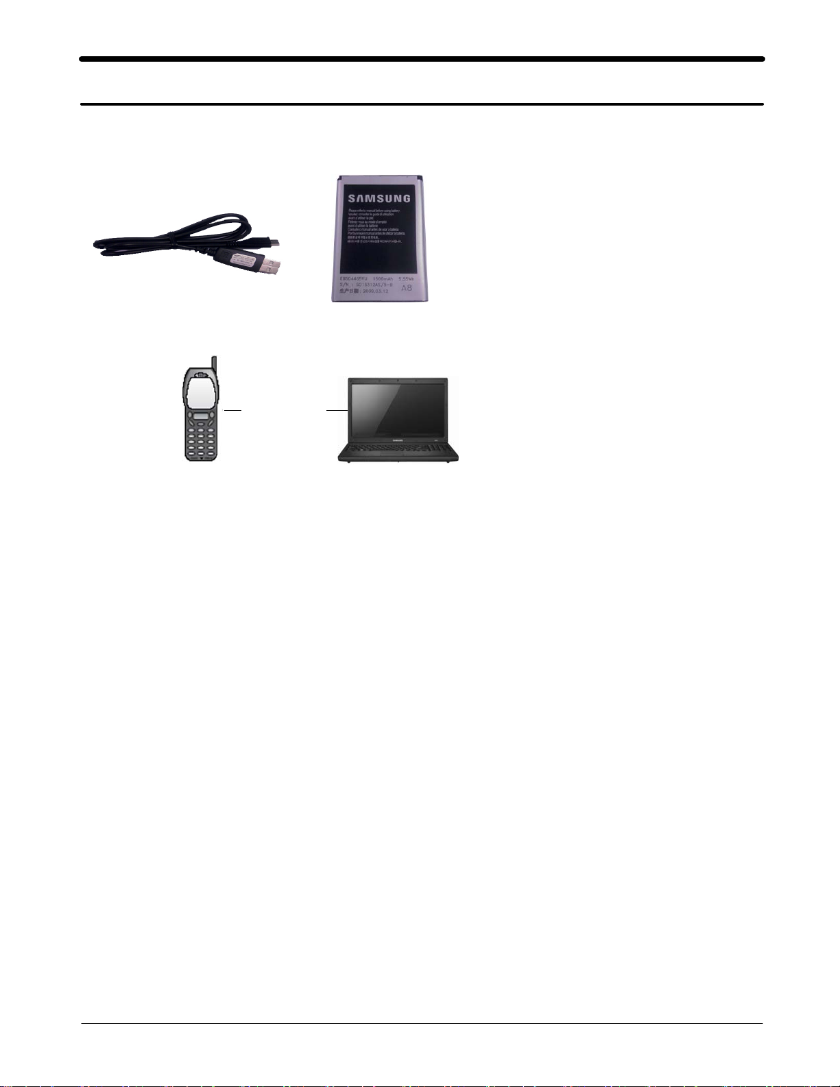
USB Cable:Because of supporting USB
1)
he device manager of your PC may not recognize the cable
that does not support USB
Battery:EB504465VU
2)
Diagram of connection
-
Data Cable
Mobile Phone(with Battery)
6
Software Download
-1.
6
Pre-requisite for Download
-1-1.
PC
2.0
2.0.
cable,
Download Program(there are2ways to download.)
•
Image Version].exe
-[
Scala_MultiDownloader_v90.exe(Mult-idownloader)
-
USB Driver
•
Samsung CDMA Modem driver[SAMSUNG_Mobile_USB_DRIVER(4.40.7.0)_v1.6.zip]
-
GT-B7330B Mobile Device
•
Binary file
•
ActiveSync Setting
•
Driver Installation.
•
s
6-1
SAMSUNG Proprietary-Contents may change without notice
This Document can not be used without Samsung's authorization
Level1Repair
6-1-2.
6-1-3.
1)
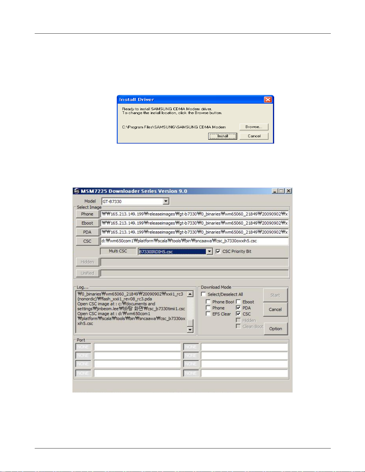
Driver Installation
Make sure that you install the driver foraphone.
You have to install the driver of Samsung CDMA Modem of downloadingaphone image
-
Restart your host PC after you install the phone driver.
-
S/W Download Process
Execute the downloader
Execute the‘Scala_MultiDownloader_v
exe’program
90.
.
Notice
(
:v90
downloader supports Multi-CSC and Single-CSC. If you select the Multi-CSC
image, you can download the one of the Single-CSC image in the Multi-CSC image)
6-2
SAMSUNG Proprietary-Contents may change without notice
This Document can not be used without Samsung's authorization
Level1Repair
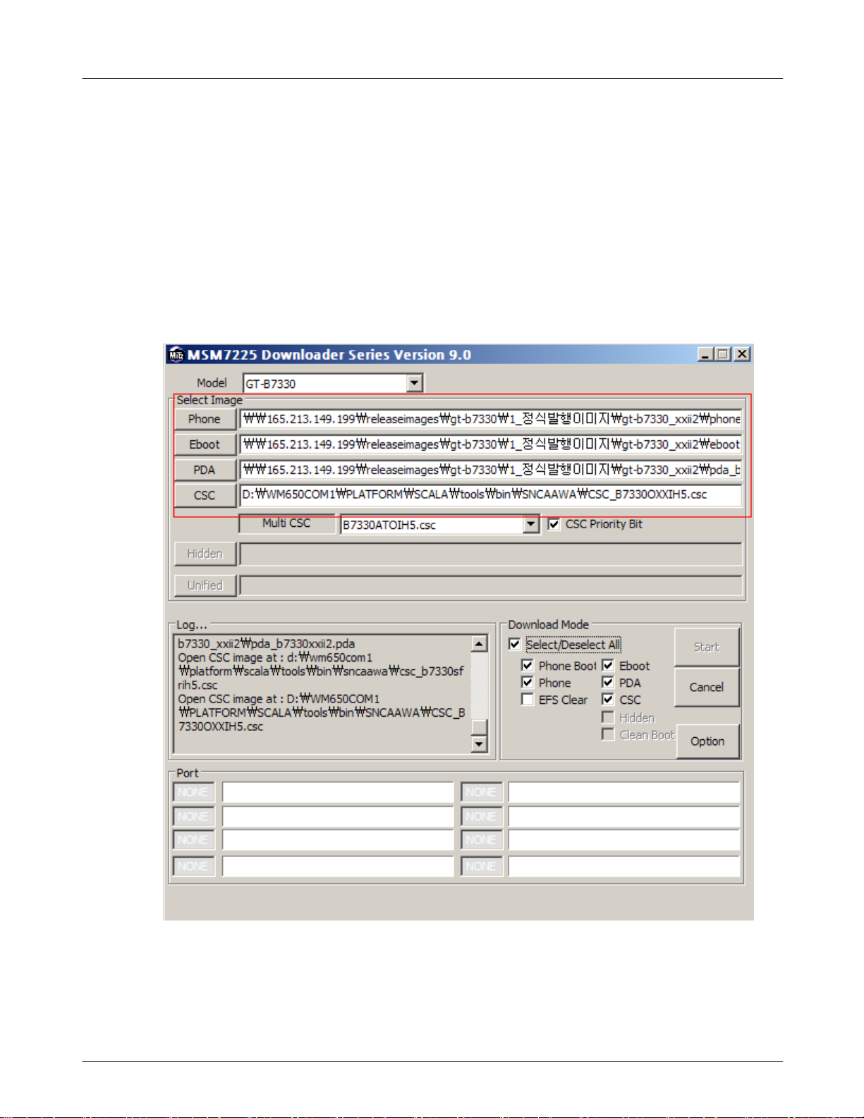
Load Image
2)
Click the“EBOOT
s
PDA”or“Phone”button, and you can select the image type.
”, “
Phone: phone_XXXXX.bin
Eboot:eboot_XXXXX.eb0
PDA: flash_XXXXX.pda
CSC: CSC_XXXX.csc
Notice:The buttons of PDA and Eboot will be activated only after phone image is add
(
ed first)
Warning:If you download PDA image, the CSC will be deleted. So, in case of need,
(
you should download CSC image again after downloading PDA image)
6-3
SAMSUNG Proprietary-Contents may change without notice
This Document can not be used without Samsung's authorization
Level1Repair
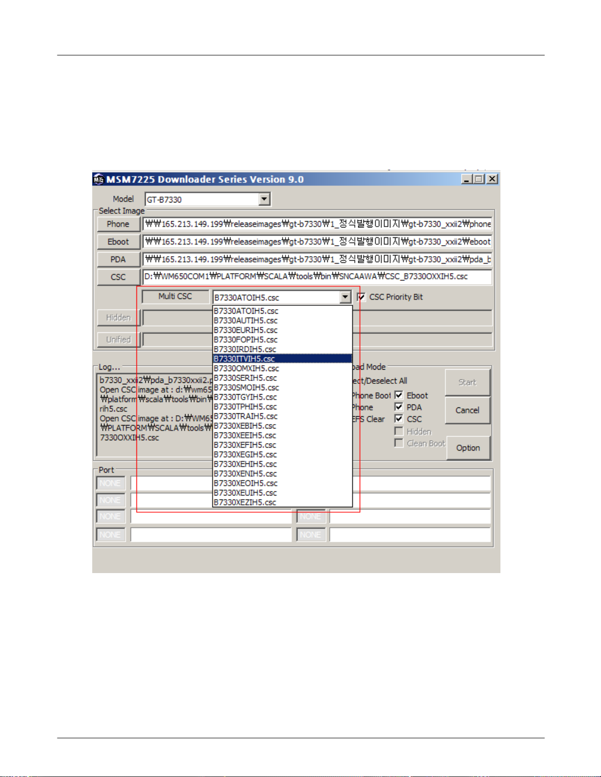
Select the CSC(in case of multi-CSC)
3)
Choose the proper CSC from the CSC.
This selection box enabled only the multi-CSC is loaded. You can pass this procedure
(
if you loadedasingle CSC file)
6-4
SAMSUNG Proprietary-Contents may change without notice
This Document can not be used without Samsung's authorization
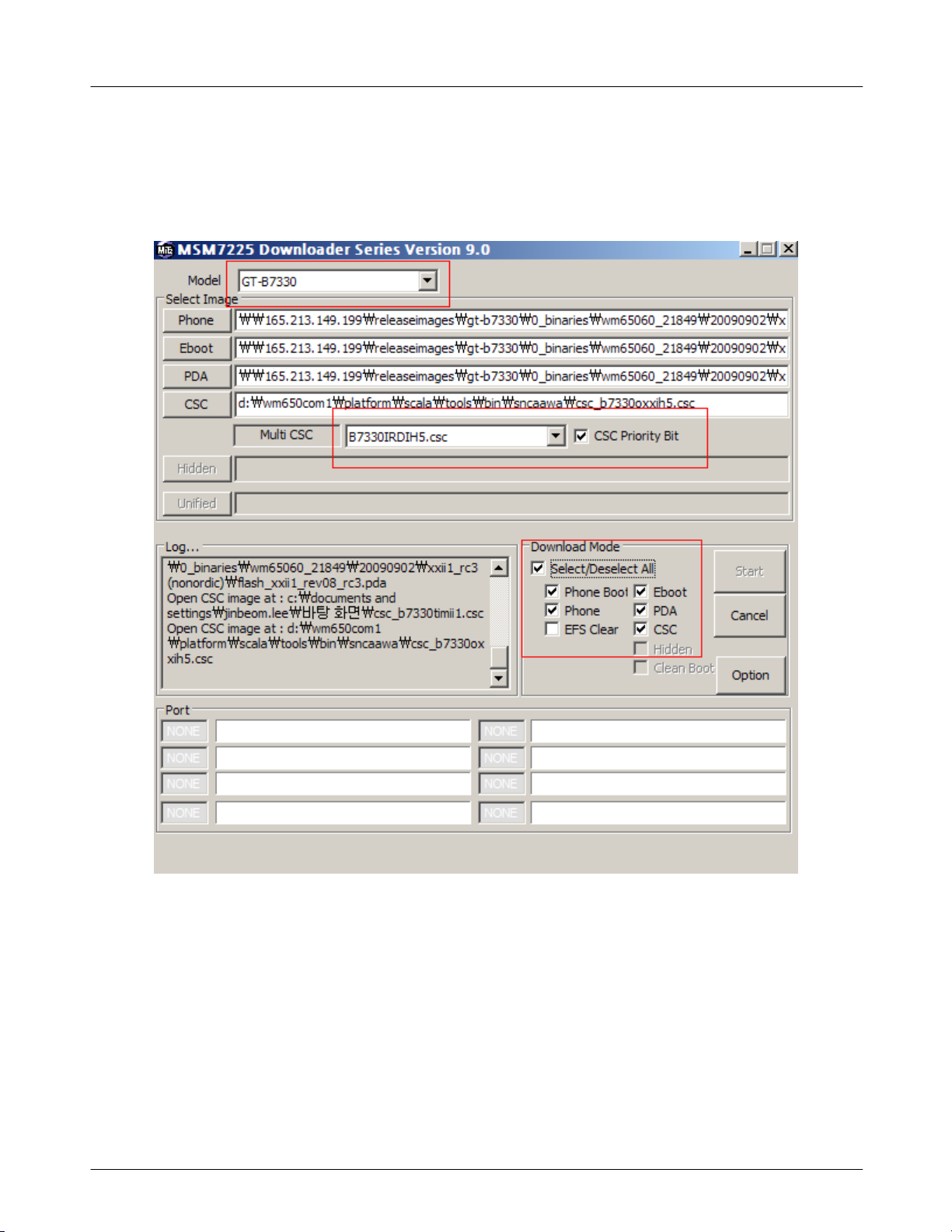
Select the download mode
4)
Check equally with part marked to red box.
Notice:Don’tcheck the‘EFS Clear
(
Level1Repair
’)
6-5
SAMSUNG Proprietary-Contents may change without notice
This Document can not be used without Samsung's authorization
Level1Repair
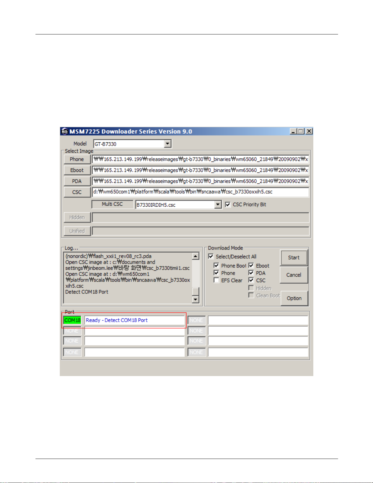
Connect thedevice
5)
First, power off the device.Second, press the
Key and connect PC with device
‘j’
using USB cable.(Don’tdetach your finger from
key.)In that case the device will po
‘j’
wer on and downloader recognize the device automatically.
The below picture shows that start button is activated and downloader is ready
to download image to device.
6-6
SAMSUNG Proprietary-Contents may change without notice
This Document can not be used without Samsung's authorization
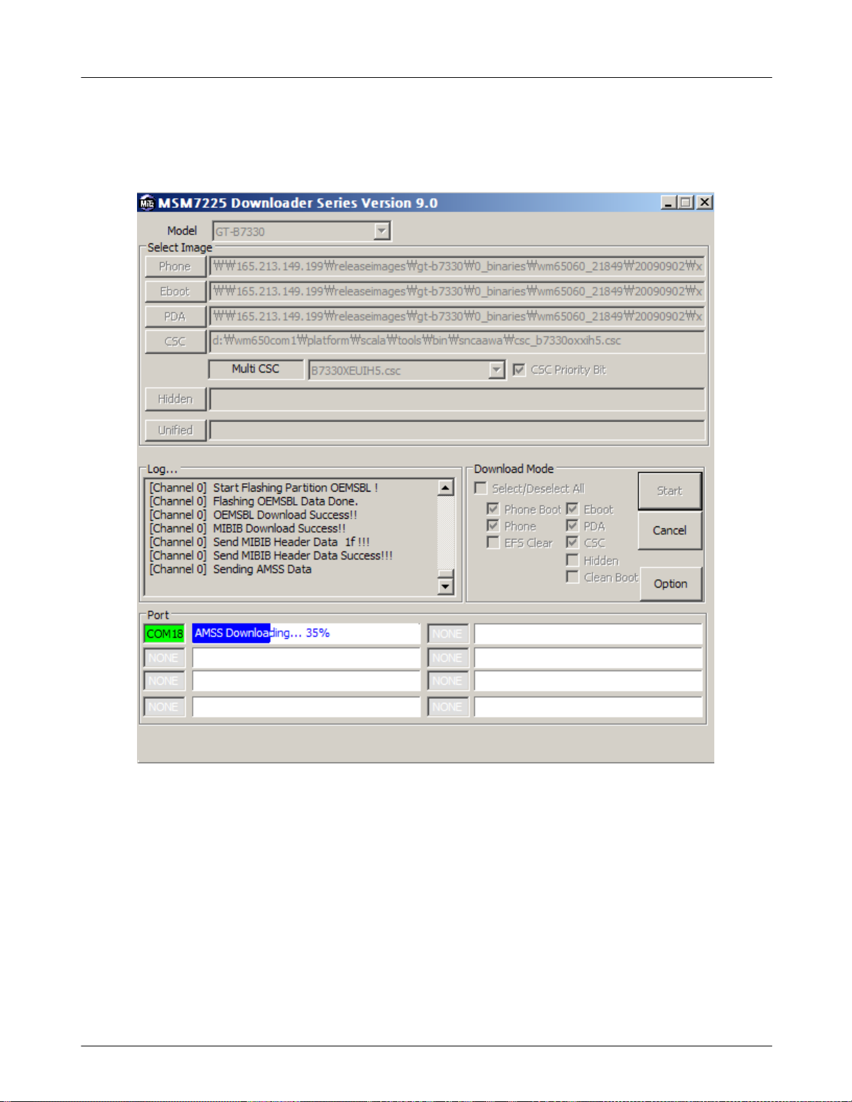
Download image
6)
Click start button and Downloader start downloading imagesto the device.
Level1Repair
s
6-7
SAMSUNG Proprietary-Contents may change without notice
This Document can not be used without Samsung's authorization
Level1Repair
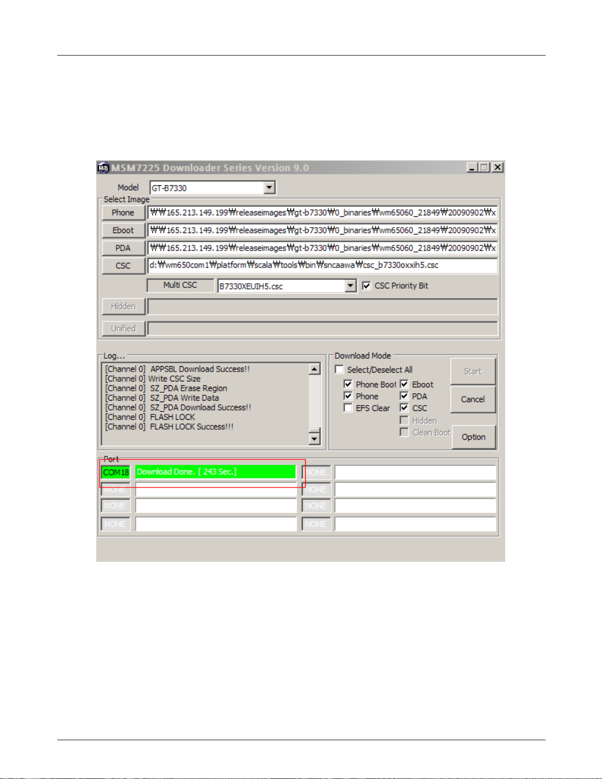
Complete download
7)
The download process is automatically executed.
phone image download
(‘
And you will be able to get the result same as below picture.
PDA image download
’->‘
’)
Notice:After download process is completed, take care of the abnormal power off situ
(
ation(ex. mount/demount battery) within the first booting time. It may causes
malfunction
Confirm Download
7)
-
-
Reboot the device and confirm whether the device do normal operation.
When completing download, downloader is automatically initialized and ready
)
for connecting next device.
6-8
SAMSUNG Proprietary-Contents may change without notice
This Document can not be used without Samsung's authorization
Level
7.
Disassembly and Assembly Instructions
7-1.
Repair
2
7-1-1.
1
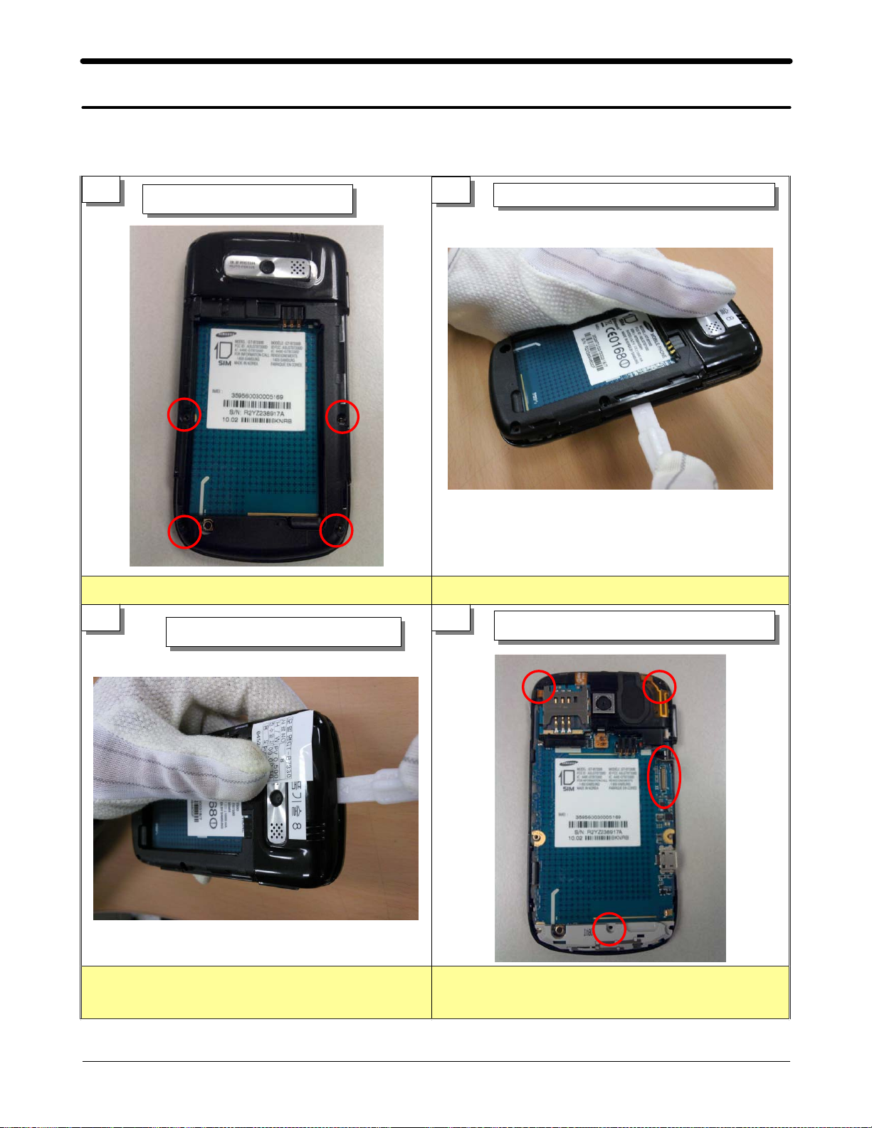
Disassembly
Unscrew REAR.
2
Disassemble REAR.
1. Unscrew SCREW 4 points. 1.Disassemble the rear from the SET's left side
3
Disassemble REAR.
1.Progress diassemble to direction of right side in
up after disassembling left side
4
1. Unscrew SCREW 2 points.
2. Disassemble LCD connector
Unscrew screw and disassemble connector
7-1
SAMSUNG Proprietary-Contents may change without notice
This Document can not be used without Samsung's authorization
Level2Repair
7.
5
Disassemble Keypad connector
1.
Disassemble connector
6
Take off Simcard connector using tweezers
1.
Disassemble Side key
2.
Disassemble connector and side key
7
1.
Detach a camera module
Push the hole using tweezers
8
Detach connectors
Detach SPK connector, Camera module and Simcard
1.
connector
7-2
SAMSUNG Proprietary-Contents may change without notice
This Document can not be used without Samsung's authorization

Level2Repair
7.
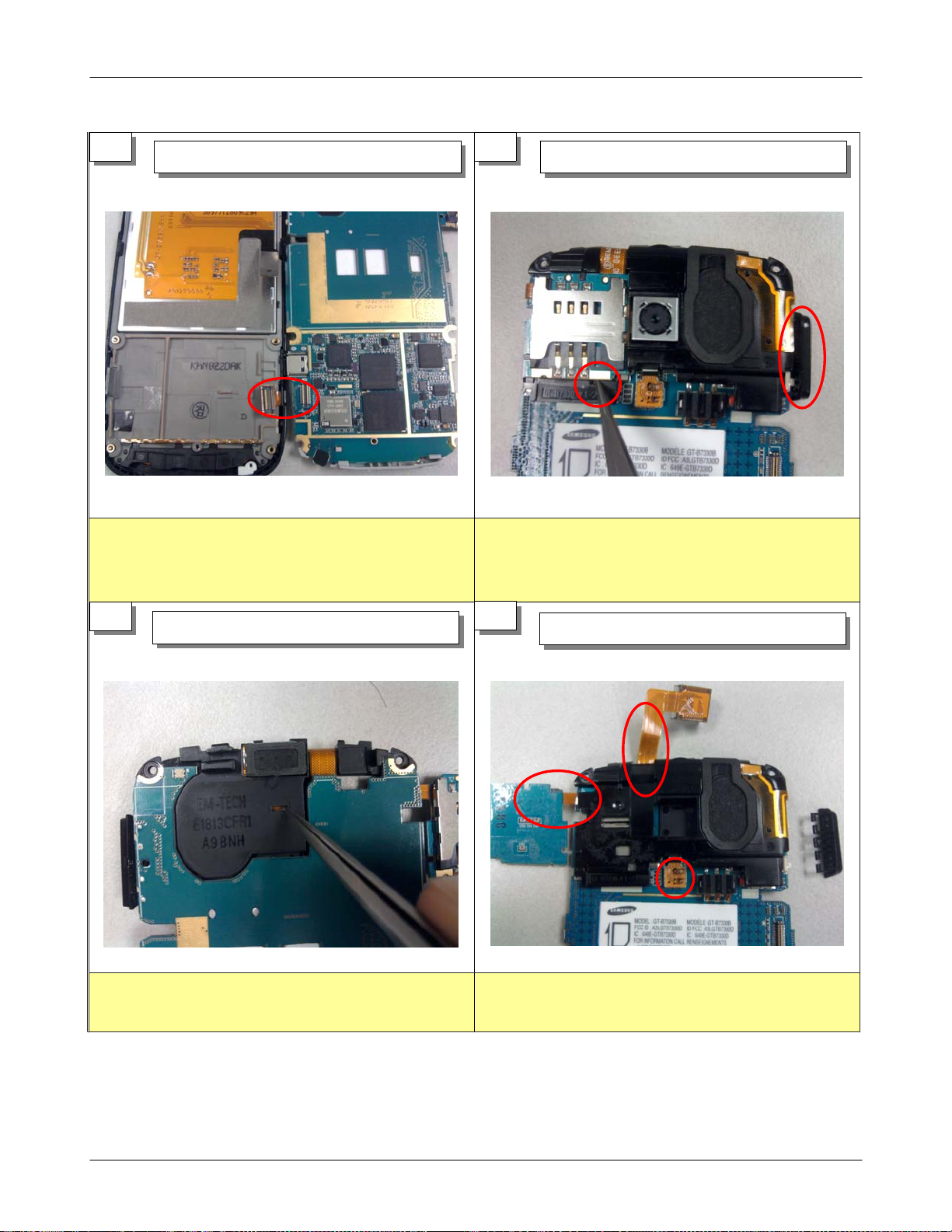
9
Disassemble two Camera modules and Simcard
1.
Disassemble connectors
connector
10
Be careful to damage of LCD and TSP unit
1.
Disassemble LCD
and remove LCD
7-3
SAMSUNG Proprietary-Contents may change without notice
This Document can not be used without Samsung's authorization
Level2Repair
7.
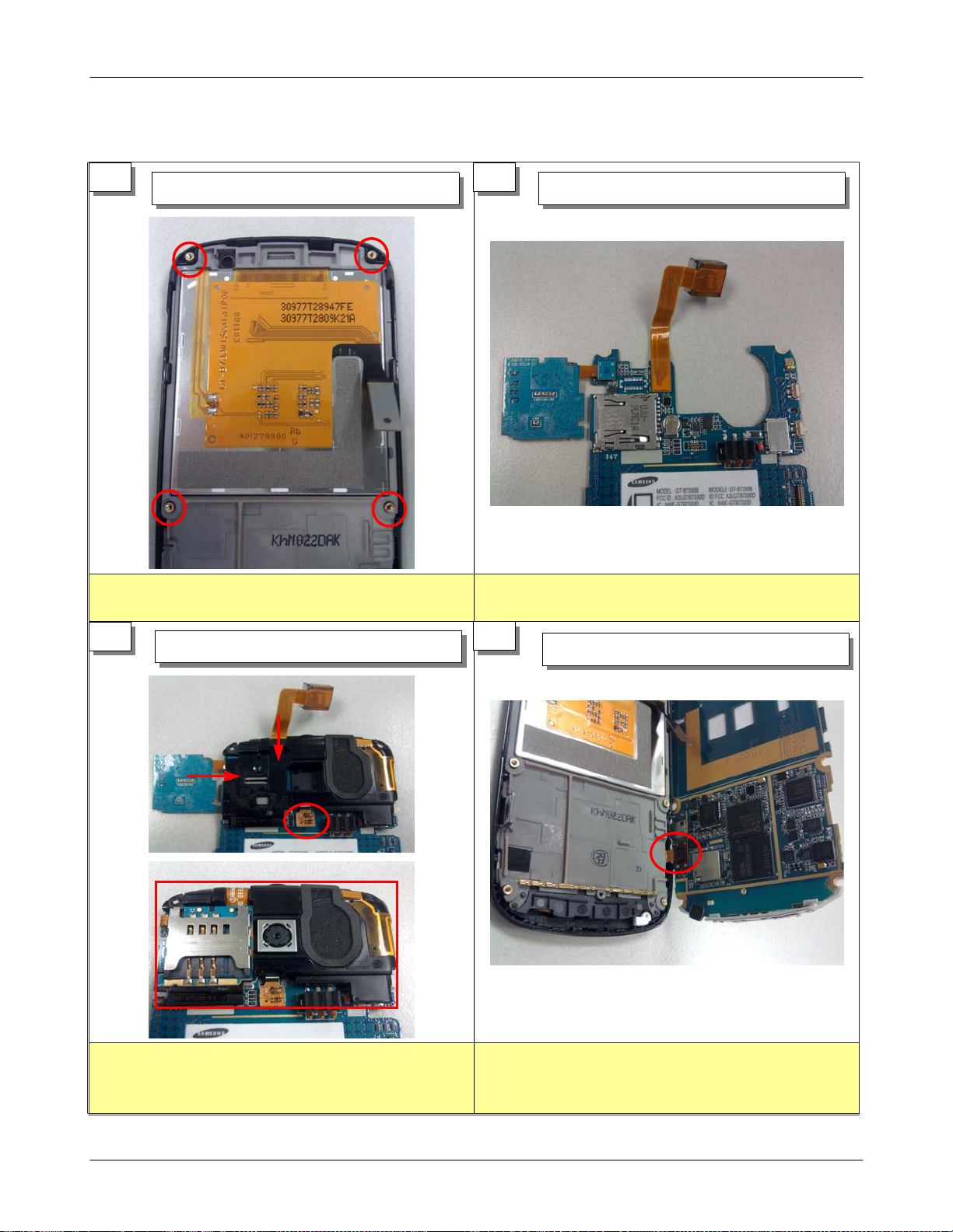
1
Assembly
Land LCD on the UPPER.
7-1-2
1. Set for UPPER's LCD place figures and assemble
LCD
2
1. Assemble two Camera modules and Simcard
connector
Assemble connectors and VOL KEY
3
1. Attach SPK connector
2. Insert Camera module
3. Attach Simcard connector
Attach connectors and module
4
Attach connector
1.Attach Keypad connector
7-4
SAMSUNG Proprietary-Contents may change without notice
This Document can not be used without Samsung's authorization
 Loading...