

Page 1

9. Flow Chart of Troubleshooting
LOGIC
9-1.
9-1-1.
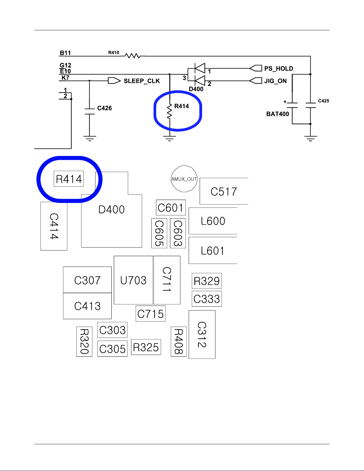
Power On
Power switch on
Check the current
consumption
>= 100
Check the battery
Check the TP_PS_
HOLD pin PS_HOL
NG
mA?
Yes
voltage
>= 3.45?
Yes
D=2.6
V?
NO
NO
NO
Download
Change the battery
Check the PMIC
relatedtoPS_HOLD
Yes
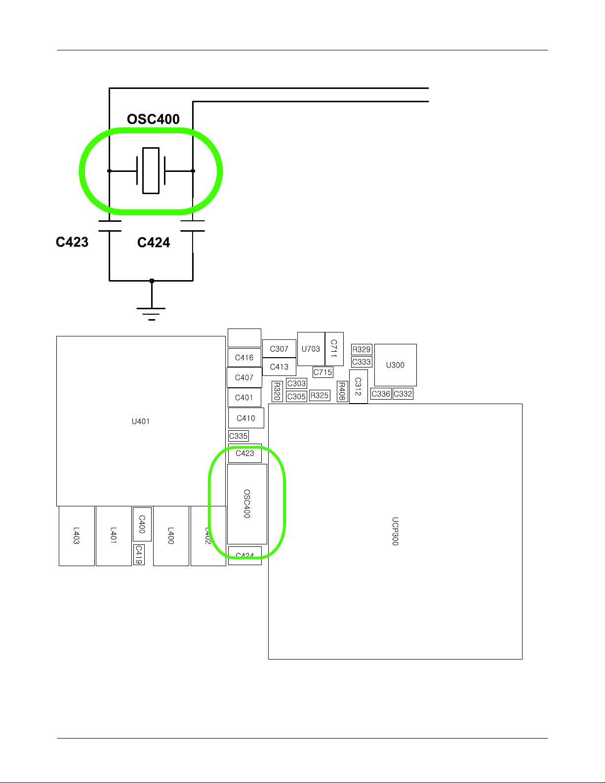
Check the clock at
OSC400
=32
KHz
?
Yes
C420(VREG_MSMC1)=1.2V?
C418(VREG_MSMC2)=1.2V?
C417(VREG_MSME)=1.8V?
C410(VREG_MSMP)=2.6V?
C409(VREG_MSMA)=2.6V?
Yes
Check the clock
C148
=19.2
Mhz
?
Yes
Check the initial operation
NO
Resolder OSC400
NO
Check the U401
NO
Check the clock generation circuit
9-1
SAMSUNG Proprietary-Contents may change without notice
This Document can not be used without Samsung's authorization
Page 2
Flow Chart of Troubleshooting
9-2
SAMSUNG Proprietary-Contents may change without notice
This Document can not be used without Samsung's authorization
Page 3

Flow Chart of Troubleshooting
9-3
SAMSUNG Proprietary-Contents may change without notice
This Document can not be used without Samsung's authorization
Page 4
Flow Chart of Troubleshooting
9-4
SAMSUNG Proprietary-Contents may change without notice
This Document can not be used without Samsung's authorization
Page 5

Flow Chart of Troubleshooting
9-5
SAMSUNG Proprietary-Contents may change without notice
This Document can not be used without Samsung's authorization
Page 6

Flow Chart of Troubleshooting
9-1-2.
LCD Working
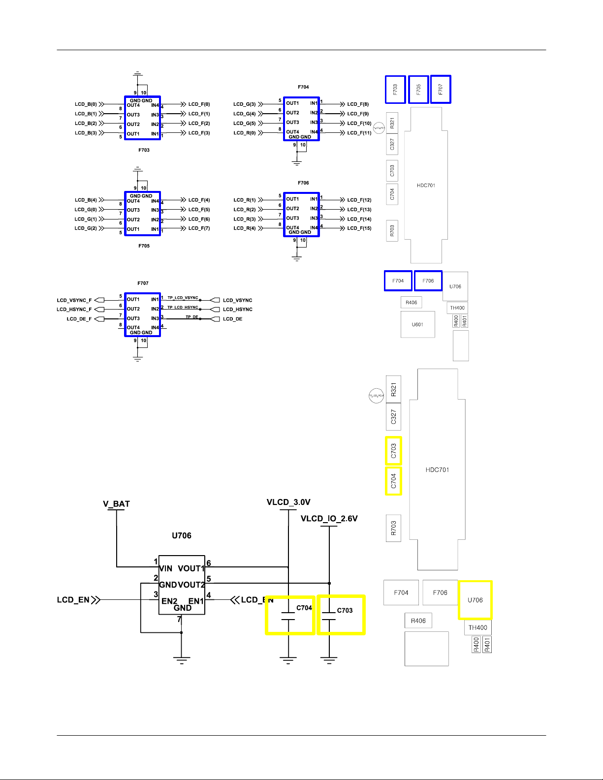
Power Switch On
LCD Display
On?
Yes
NO
LCD FPCB
connector is co
rrectly connecti
ng?
Yes
F703, F704,
F705, F706,
F707 Correctly
mounted?
Yes
NO
NO
correctly connect
F703, F704, F705,
F706, F707
Resolder
Yes
LCD
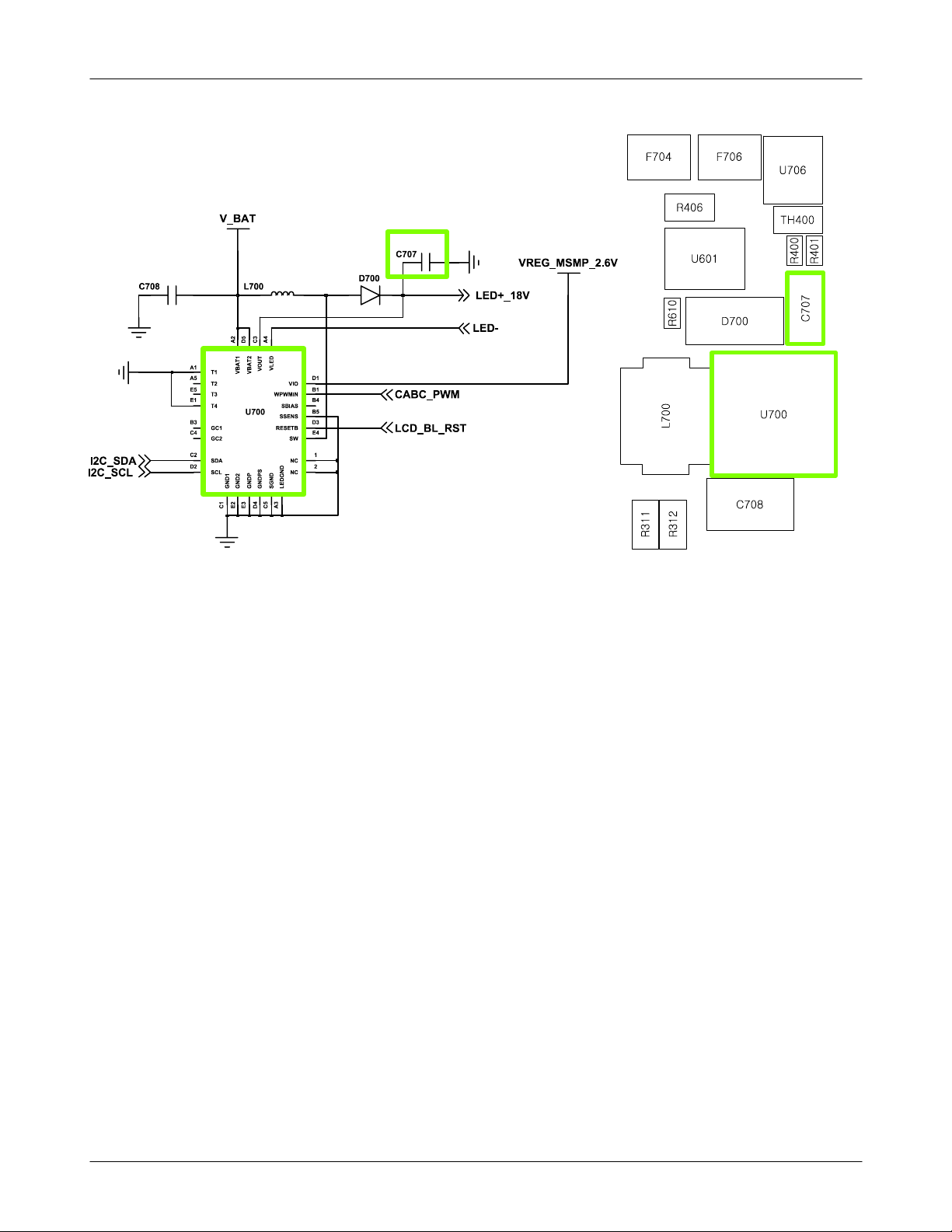
Replace
C707
LED+_18V=18V?
NO
Replace U700&Check
neighboring circuits
Yes
9-6
Yes
U706
Replace
C704, C703
VLCD_IO_2.6=2.6V
VLCD_3.0V
=3.0V
NO
U706
rd,4th pin
3
LCD_EN=High
NO
Change
Main PBA
SAMSUNG Proprietary-Contents may change without notice
This Document can not be used without Samsung's authorization
Page 7
Flow Chart of Troubleshooting
9-7
SAMSUNG Proprietary-Contents may change without notice
This Document can not be used without Samsung's authorization
Page 8
Flow Chart of Troubleshooting
9-8
SAMSUNG Proprietary-Contents may change without notice
This Document can not be used without Samsung's authorization
Page 9

Flow Chart of Troubleshooting
9-1-3.
z
Audio Working
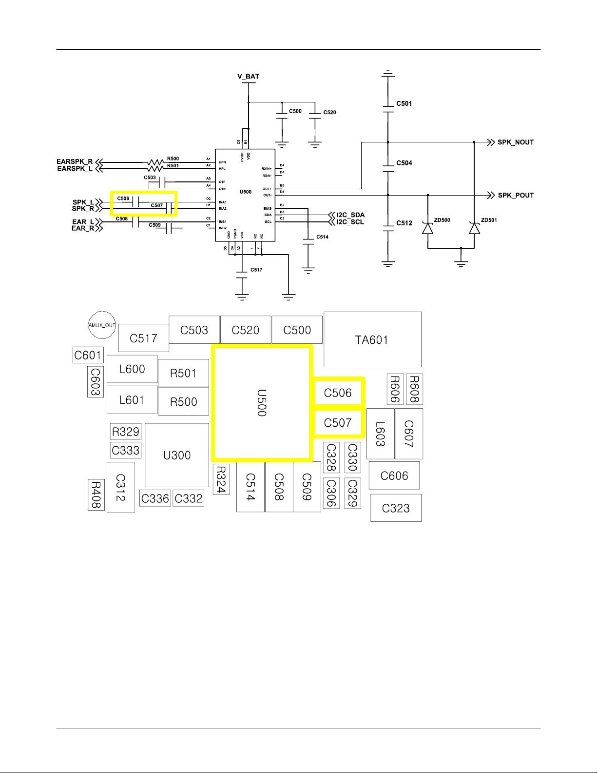
Speaker(Receiver) Working
Operate speaker
NG
Connect
Speaker Module
FPCB correctly?
YES
Speaker break
down?
NO
NO
YES
Connect correctly
Change speaker
ASSY
Signal on in
C501,C512
SPK mode)/
(
C502,C513
RCV mode)?
(
NO
Signal on in
C506, C507
SPK mode)?
(
NO
YES
YES
SPK ASSY
FPCB break
down?
NO
Check
RCV mode) pins in
7,9(
SPK mode)
1,3(
HEA500
Replace U600
YES
Change
SPK ASSY
/
Change main PBA
SAMSUNG Proprietary-Contents may change without notice
This Document can not be used without Samsung's authorization
9-9
Page 10

Flow Chart of Troubleshooting
9-10
SAMSUNG Proprietary-Contents may change without notice
This Document can not be used without Samsung's authorization
Page 11
Flow Chart of Troubleshooting
9-11
SAMSUNG Proprietary-Contents may change without notice
This Document can not be used without Samsung's authorization
Page 12

Flow Chart of Troubleshooting
z
MICW
orking
Operate MIC
NG
Insert
MIC rubber
correctly?
YES
Pollute
MIC Hole?
NO
YES
Insert correctly
Clean up
MIC hole
NO
Check
C516=High?
YES
Change MIC
NO
Remove MIC,
Check MIC5th pin
MIC_BIAS_1.8V)
(
=1.8V?
YES
Change MIC
NO
Change main PBA
9-12
SAMSUNG Proprietary-Contents may change without notice
This Document can not be used without Samsung's authorization
Page 13

Flow Chart of Troubleshooting
9-13
SAMSUNG Proprietary-Contents may change without notice
This Document can not be used without Samsung's authorization
Page 14

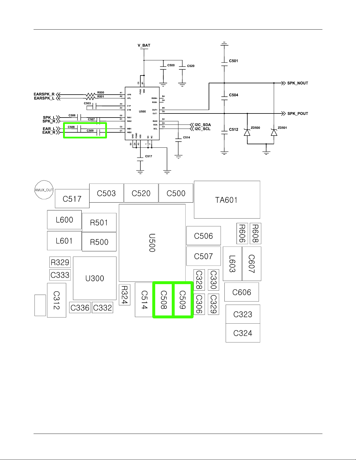
z
Hands-Free Stereo Headset Working
Hands-free stereo
headset
NG
YES
Button NG?
NO
Flow Chart of Troubleshooting
Check U707&U600
MIC NG?
NO
SPK NG?
NO
The End
YES
YES
Check
R606
=1.8
V?
YES
Check U707&U600
Signal on
in C601,
C605?
NO
Signal on
in C508,
C509?
NO
NO
Check U703
YES
Check U707&U600
YES
Check U500
Change Main PBA
9-14
SAMSUNG Proprietary-Contents may change without notice
This Document can not be used without Samsung's authorization
Page 15

Flow Chart of Troubleshooting
9-15
SAMSUNG Proprietary-Contents may change without notice
This Document can not be used without Samsung's authorization
Page 16

Flow Chart of Troubleshooting
9-16
SAMSUNG Proprietary-Contents may change without notice
This Document can not be used without Samsung's authorization
Page 17
Flow Chart of Troubleshooting
9-17
SAMSUNG Proprietary-Contents may change without notice
This Document can not be used without Samsung's authorization
Page 18

Flow Chart of Troubleshooting
9-1-4.
z
KEY Working
Navi KEY
Press Navi Key
All key NG?
UP/DOWN NG?
NG
YES
Change Front Ass'y(Key FPCB)
NO
YES
Check R507, R508
NO
Acceleration NG?
NO
END
YES
Check ZD509, ZD510
9-18
SAMSUNG Proprietary-Contents may change without notice
This Document can not be used without Samsung's authorization
Page 19

Flow Chart of Troubleshooting
9-19
SAMSUNG Proprietary-Contents may change without notice
This Document can not be used without Samsung's authorization
Page 20

POWER KEY, VOLUME KEY, MAIN KEY PART
z
Press Power key,
Volume Key, Main Key
Flow Chart of Troubleshooting
Power Key NG?
NO
Volume Key
NG?
NO
Yes
Yes
Pressing
power key,
R506=High?
NO
Change Front Ass'y
st pin of TAC500,
1
TAC501=High
Yes
Pressing Vol key
ZD505, ZD506
High
=
?
NO
Check TAC500, TAC501
Yes
NO
Yes
Check U501
Neighboring Circuits
&
Change Main PBA
Change Main PBA
QWERTY Key
NG?
NO
The End
Yes
Key FPCB
Disconnect or
Break Down
?
Yes
NO
Check HEA501
Neighboring Circuits
&
9-20
SAMSUNG Proprietary-Contents may change without notice
This Document can not be used without Samsung's authorization
Connect correctly or
Change Front Ass'y
Page 21

Flow Chart of Troubleshooting
9-21
SAMSUNG Proprietary-Contents may change without notice
This Document can not be used without Samsung's authorization
Page 22

Flow Chart of Troubleshooting
9-1-5.
Vibrator Working
Operate Vibrator
Connect SPK Mo
dule correctly?
Check C510
=3.3V?
NO
Yes
Yes
NO
Connect correctly
Check D500, TA500
Neighboring Circuit
&
rd pin in
3
High?
=
Change PBA
NO
U704
NO
Yes
Change U704
9-22
SAMSUNG Proprietary-Contents may change without notice
This Document can not be used without Samsung's authorization
Page 23

Flow Chart of Troubleshooting
9-23
SAMSUNG Proprietary-Contents may change without notice
This Document can not be used without Samsung's authorization
Page 24

Flow Chart of Troubleshooting
9-24
SAMSUNG Proprietary-Contents may change without notice
This Document can not be used without Samsung's authorization
Page 25

Flow Chart of Troubleshooting
9-1-6.
T-Flash Card Working
Insert&Operate
microSD card
CD400
break down
C434
High
=
NG
NO
?
?
YES
Change CD400
Change CD400
YES
NO
C434
=3.0V?
YES
Check F501
Neighboring Circuit
&
Change U500(PMIC)
NO
9-25
SAMSUNG Proprietary-Contents may change without notice
This Document can not be used without Samsung's authorization
Page 26

Flow Chart of Troubleshooting
9-26
SAMSUNG Proprietary-Contents may change without notice
This Document can not be used without Samsung's authorization
Page 27

9. Flow Chart of Troubleshooting
9-27
SAMSUNG Proprietary-Contents may change without notice
This Document can not be used without Samsung's authorization
Page 28

Flow Chart of Troubleshooting
9-1-7.
SIM Card Working
Insert&Operate
Connect FPCB
SIM FPCB
Break down?
SIM card
correctly
NG
?
YES
NO
Connect correctly
YES
Change SIM FPCB
NO
C431
=3.0V?
YES
Check SIM400
Neighboring Circuits
&
NO
Change U500(PMIC)
9-28
SAMSUNG Proprietary-Contents may change without notice
This Document can not be used without Samsung's authorization
Page 29

Flow Chart of Troubleshooting
9-29
SAMSUNG Proprietary-Contents may change without notice
This Document can not be used without Samsung's authorization
Page 30

Flow Chart of Troubleshooting
9-1-8
CAMERA Working
Operate CAMERA
NG
Camera FPCB con
nector is correctly
connecting?
Yes
F700, F701, F702
Correctly mounted?
Yes
C712,C713
VCAM_28V_IO=2.8V
VCAM_18C=1.8V?
,
NO
NO
NO
correctly connect
F700, F701, F702 Resolder
U701
rd pin CAM_EN
3
High?
=
NO
Yes
C705
VCAM_28A=2.8V
Yes
CAMERA
Replace
NO
U702
rd pin
3
CAM_EN=High?
Yes
U702
Replace
Yes
NO
U701
Replace
UCP300
Replace
9-30
SAMSUNG Proprietary-Contents may change without notice
This Document can not be used without Samsung's authorization
Page 31

Flow Chart of Troubleshooting
9-31
SAMSUNG Proprietary-Contents may change without notice
This Document can not be used without Samsung's authorization
Page 32

Flow Chart of Troubleshooting
9-32
SAMSUNG Proprietary-Contents may change without notice
This Document can not be used without Samsung's authorization
Page 33

Flow Chart of Troubleshooting
RF
9-2.
9-2-1.
**
GSM
If you check the tx chain,
Check the not only RF Device but also resistor, inductor and capacitor.
850
Receiver
Continous Rx ON
RF Input
Amplitude
: 190
:-50
CH
dBm
Yes
No
Normal condition
Catch the channel?
Check Antenna contact
Yes
Check L110
=-55
dBm
?
Yes
Resolder U100 or Change
Yes
The End
No
Replace RFS101
9-33
SAMSUNG Proprietary-Contents may change without notice
This Document can not be used without Samsung's authorization
Page 34

RFS100
G
G
4
3
Flow Chart of Troubleshooting
C
A
2
1
C102
VREG_SYNTH_2.7V
L106L105
11
GSM850|900TX GSM850RX
9
GSM1800|1900TX
3
VC1
4
VC2
5
VC3
6
VC4
RFS101
C103
7
2
T
D
N
D
A
V
12
13
GSM850RX
14
GSM900RX
15
GSM900RX
16
GSM1800RX
17
GSM1800RX
18
GSM1900RX
19
GSM1900RX
20
UMTS1
21
UMTS2
22
UMTS3
G
G
G
G
G
4
3
0
8
1
1
2
2
L108
L112
C157
L117
L107
L109
L111
L113
L123
L124
C108
C109
L110
L114
L116
L118
RX_GSM850_N
RX_GSM850_P
RX_EGSM900_N
RX_EGSM900_P
RX_DCS1800_N
RX_DCS1800_P
RX_PCS1900_N
RX_PCS1900_P
TXR_WCDMA2100
TXR_WCDMA900
9-34
SAMSUNG Proprietary-Contents may change without notice
This Document can not be used without Samsung's authorization
Page 35

Flow Chart of Troubleshooting
9-2-2.
**
GSM
If you check the tx chain,
Check the not only RF Device but also resistor, inductor and capacitor.
Transmitter
850
Tx ON(Level
:5)
Battery voltage:3.8V
Yes
No
Check C121
>= 14
dBm?
Yes
Check The U100
Check C100
Check C102
The End
>= 34.5
Yes
>= 33
dBm?
Yes
dBm?
No
Replace PAM100
No
Replace RFS101
9-35
SAMSUNG Proprietary-Contents may change without notice
This Document can not be used without Samsung's authorization
Page 36

2
2
1
1
ANT101
C165
GSM850_900
GSM1800_1900
GSM_ANT_SEL0_N
GSM_ANT_SEL1_N
GSM_ANT_SEL2_N
GSM_ANT_SEL3_N
PAM_RFOUT_G850_EGSM
PAM_RFOUT_DCS_PCS
GSM_PA_EN
GSM_PA_BAND
GSM_PA_RAMP+
RFS100
G
G
C
A
4
3
2
1
C101
C106
R114
R115
R116
R117
C102
L106L105
11
GSM850|900TX GSM850RX
9
GSM1800|1900TX
3
VC1
4
VC2
5
VC3
6
VC4
2
7
T
N
A
G
G
G
3
1
0
8
2
1
RFS101
D
D
V
GSM850RX
GSM900RX
GSM900RX
GSM1800RX
GSM1800RX
GSM1900RX
GSM1900RX
G
G
4
2
UMTS1
UMTS2
UMTS3
12
13
14
15
16
17
18
19
20
21
22
V_BAT
TA100
4
T
T
R107
8
1
3
2
5
GSM_IN GSM_OUT
DCS|PCS_IN
TX_EN
BAND_SEL
VRAMP
R101
R100
R103 C104
C105
R104
R105
R106
A
B
V
DCS|PCS_OUT
D
D
N
N
G
G
2
7
1
9
11
6
NC
10
NC
PAM100
L100
C100
L102
L101
L103
GSM850_900
GSM1800_1900
Flow Chart of Troubleshooting
C137
10
11
12
13
14
15
16
17
1
2
3
4
5
6
7
8
9
R108
1
7
VDDA2
TCXO
VDDA1
VDDA1
VTUNE1
VDDA1
VDDA2
VDDA2
VTUNE_GPS
VDDA1
PRX_QP
PRX_QN
PRX_IN
PRX_IP
DRX_QP
DRX_QN
DRX_IP
VREG_PA_2.1V
VREG_RFRX1_2.7V
C163
C159
1
IN
G
C144
25
C115
C116
PAM_RFOUT_W2100
PAM_RFOUT_W900
PAM_RFOUT_DCS_PCS
PAM_RFOUT_G850_EGSM
PWR_DET
RTR_W2100_RX
F100
3
OUT
4
OUT
G
L120
C138
C141
VREG_PA_2.1V
C127
WCDMA_RXM_2100
WCDMA_RXP_2100
C134
C111
C113
C156
C120
C131
C135
RTR_W900_M
RTR_W900_P
WCDMA_RXM_2100
WCDMA_RXP_2100
C117
C121
RX_GSM850_N
RX_GSM850_P
RX_EGSM900_N
RX_EGSM900_P
RX_DCS1800_N
RX_DCS1800_P
RX_PCS1900_N
RX_PCS1900_P
RX_GPS
C132
C160
C122
C133
R113
L119
C139
C119
6
4
5
7
9
0
8
6
6
6
6
7
6
F
P
S
C
C
G
E
A
Q
N
N
U
I
_
R
L
I
B
X
S
_
R
_
T
C
_
D
A
X
N
T
D
G
N
2
1
I
A
_
A
T
X
D
D
D
C
|
R
D
B
D
S
V
V
D
N
2
0
1
3
8
9
2
2
2
2
1
1
2
3
6
6
6
2
P
N
N
I
I
A
Q
_
_
D
_
X
X
X
D
T
T
T
V
U100
2
2
E
N
A
M
N
O
D
D
_
U
F
D
T
D
V
V
V
R
4
5
6
2
2
2
N
O
_
X
T
C143
7
8
9
0
1
6
6
2
A
D
D
V
2
A
D
D
V
8
7
2
2
2
3
4
5
6
5
5
5
5
5
5
5
5
1
N
2
3
1
1
2
2
2
I
A
_
T
T
T
T
T
A
A
D
T
D
U
U
U
E
U
U
D
D
V
D
O
O
O
O
O
D
D
P
51
_
_
_
_
_
V
V
GCELL_INN
F
F
F
F
F
50
R
R
R
R
R
GCELL_INP
_
_
_
_
_
49
B
B
B
B
B
EGSM_INN
L
L
H
H
H
P
M
N
N
P
I
I
M
_
_
B
B
X
X
L
L
X
X
M
M
_
_
R
R
B
B
P
P
W
W
W
W
9
0
1
2
3
3
48
EGSM_INP
47
DCS_INN
46
DCS_INP
45
GPCS_INN
44
GPCS_INP
43
VDDA2
42
GPS_IN
C130
41
WDRXLB
40
WDRXHB1
39
WDRXHB2
38
WPRXSE1
37
VDDA2
36
T
P
WPRXSE2
U
B
O
35
_
WPRXSE1_OUT
H
M
2
B
E
X
H
S
R
X
X
R
R
P
P
P
W
W
W
2
3
4
3
3
3
C158
C161
L125
C162
9-36
SAMSUNG Proprietary-Contents may change without notice
This Document can not be used without Samsung's authorization
Page 37

Flow Chart of Troubleshooting
9-37
SAMSUNG Proprietary-Contents may change without notice
This Document can not be used without Samsung's authorization
Page 38

Flow Chart of Troubleshooting
9-2-3.
**
GSM
If you check the tx chain,
Check the not only RF Device but also resistor, inductor and capacitor.
900
Receiver
Continous Rx ON
RF Input
Amplitude
:62
:-50
CH
dBm
Yes
No
Normal Condition
Catch the channel?
Yes
Check Antenna Contact
Check L114
>= -55
dBm?
Yes
Resolder U100 or Change
The End
No
Replace RFS101
9-38
SAMSUNG Proprietary-Contents may change without notice
This Document can not be used without Samsung's authorization
Page 39

Flow Chart of Troubleshooting
RFS100
G
C
A
G
1
4
2
3
VREG_SYNTH_2.7V
C102
L106L105
11
GSM850|900TX GSM850RX
9
GSM1800|1900TX
3
VC1
4
VC2
5
VC3
6
VC4
RFS101
C103
7
2
T
D
N
D
A
V
12
13
GSM850RX
14
GSM900RX
15
GSM900RX
16
GSM1800RX
17
GSM1800RX
18
GSM1900RX
19
GSM1900RX
20
UMTS1
21
UMTS2
22
UMTS3
G
G
G
G
G
1
0
4
3
8
1
2
2
L108
L112
C157
L117
L107
L109
L111
L113
L123
L124
C108
C109
L110
L114
L116
L118
RX_GSM850_N
RX_GSM850_P
RX_EGSM900_N
RX_EGSM900_P
RX_DCS1800_N
RX_DCS1800_P
RX_PCS1900_N
RX_PCS1900_P
TXR_WCDMA2100
TXR_WCDMA900
9-39
SAMSUNG Proprietary-Contents may change without notice
This Document can not be used without Samsung's authorization
Page 40

Flow Chart of Troubleshooting
9-2-4.
**
GSM900 Transmitter
If you check the tx chain,
Check the not only RF Device but also resistor, inductor and capacitor.
Tx ON(Level
:5)
Battery voltage:3.8V
Yes
No
Check C121
=14
dBm?
Yes
Check The U100
Check C100
Check C102
The End
>= 34.5
Yes
>= 33
dBm?
Yes
dBm?
No
Replace PAM100
No
Replace RFS102
9-40
SAMSUNG Proprietary-Contents may change without notice
This Document can not be used without Samsung's authorization
Page 41

Flow Chart of Troubleshooting
RFS100
C
A
G
C106
C101
G
2
1
3
4
R101
C105
R105
R104
2
2
1
1
ANT101
GSM850_900
GSM1800_1900
GSM_ANT_SEL0_N
GSM_ANT_SEL1_N
GSM_ANT_SEL2_N
GSM_ANT_SEL3_N
PAM_RFOUT_G850_EGSM
PAM_RFOUT_DCS_PCS
GSM_PA_EN
GSM_PA_BAND
GSM_PA_RAMP+
C165
R114
R115
R116
R117
R103 C104
C102
L106L105
11
GSM850|900TX GSM850RX
9
GSM1800|1900TX
3
VC1
4
VC2
5
VC3
6
VC4
RFS101
R100
R106
R107
7
2
T
D
N
D
A
V
GSM850RX
GSM900RX
GSM900RX
GSM1800RX
GSM1800RX
GSM1900RX
GSM1900RX
G
G
G
G
G
1
0
4
3
8
1
2
2
8
GSM_IN GSM_OUT
1
DCS|PCS_IN
3
TX_EN
2
BAND_SEL
5
VRAMP
UMTS1
UMTS2
UMTS3
4
T
T
A
B
V
DCS|PCS_OUT
D
D
N
N
G
G
2
7
1
12
13
14
15
16
17
18
19
20
21
22
9
11
6
NC
10
NC
PAM100
V_BAT
TA100
L100
L101
C100
L102
GSM850_900
GSM1800_1900
L103
C137
1
2
3
4
5
6
7
8
9
10
11
12
13
14
15
16
17
VDDA2
TCXO
VDDA1
VDDA1
VTUNE1
VDDA1
VDDA2
VDDA2
VTUNE_GPS
VDDA1
PRX_QP
PRX_QN
PRX_IN
PRX_IP
DRX_QP
DRX_QN
DRX_IP
R108
1
7
VREG_PA_2.1V
VREG_RFRX1_2.7V
C163
C159
1
IN
C144
C115
C116
PAM_RFOUT_W2100
PAM_RFOUT_W900
PAM_RFOUT_DCS_PCS
PAM_RFOUT_G850_EGSM
PWR_DET
F100
3
OUT
4
OUT
G
G
25
RTR_W2100_RX
C138
L120
C141
VREG_PA_2.1V
C127
WCDMA_RXM_2100
WCDMA_RXP_2100
C134
C111
C120
C131
C135
RTR_W900_M
RTR_W900_P
WCDMA_RXM_2100
WCDMA_RXP_2100
C117
C121
RX_GSM850_N
RX_GSM850_P
RX_EGSM900_N
RX_EGSM900_P
RX_DCS1800_N
RX_DCS1800_P
RX_PCS1900_N
RX_PCS1900_P
RX_GPS
C132
C160
C119
8
4
5
6
7
9
0
2
3
6
6
6
6
6
6
7
6
6
2
F
P
P
N
N
S
C
C
G
I
I
A
E
A
Q
N
N
Q
U
_
_
I
_
D
R
_
L
X
X
I
B
X
X
D
S
T
T
_
R
T
_
T
V
C
_
D
A
X
N
T
D
G
U100
2
N
2
1
2
E
N
I
A
A
M
A
_
T
N
O
X
D
D
D
D
D
_
U
C
F
R
|
B
D
D
D
T
D
S
V
V
V
V
V
R
D
N
0
1
2
3
4
5
6
8
9
2
2
2
2
2
2
2
1
1
N
O
_
X
T
C143
3
7
8
9
0
1
6
2
A
D
D
V
2
A
D
D
V
7
2
2
4
5
6
5
5
5
6
5
5
5
5
5
1
N
3
1
2
2
1
2
2
I
A
_
T
T
T
T
T
A
A
D
T
D
U
U
U
E
U
U
D
D
V
D
O
O
O
O
O
D
D
P
51
_
_
_
_
_
V
V
GCELL_INN
F
F
F
F
F
50
R
R
R
R
R
GCELL_INP
_
_
_
_
_
B
B
B
H
H
M
P
N
N
I
I
P
_
_
B
X
X
L
X
M
M
_
R
_
B
B
P
W
W
W
8
9
0
1
2
2
3
3
49
B
B
EGSM_INN
L
L
H
48
EGSM_INP
47
DCS_INN
46
DCS_INP
45
GPCS_INN
44
GPCS_INP
43
VDDA2
42
GPS_IN
C130
41
WDRXLB
40
WDRXHB1
39
WDRXHB2
38
WPRXSE1
37
VDDA2
36
T
P
WPRXSE2
M
U
B
O
B
35
_
WPRXSE1_OUT
L
H
M
2
B
E
X
X
S
H
R
R
X
X
R
R
P
P
P
P
W
W
W
W
2
3
4
3
3
3
C158
C161
L125
C162
C113
C156
C122
C133
L119
R113
C139
9-41
SAMSUNG Proprietary-Contents may change without notice
This Document can not be used without Samsung's authorization
Page 42

Flow Chart of Troubleshooting
9-42
SAMSUNG Proprietary-Contents may change without notice
This Document can not be used without Samsung's authorization
Page 43

Flow Chart of Troubleshooting
9-2-5.
**
DCS1
If you check the tx chain,
Check the not only RF Device but also resistor, inductor and capacitor.
800
Receiver
Continous Rx ON
RF Input
Amplitude
:698
:-50
CH
dBm
Yes
No
Normal Condition
Catch the channel?
Yes
Check Antenna Contact
Check L116
>= -55
dBm?
Yes
Resolder U100 or Change
The End
No
Replace RFS101
9-43
SAMSUNG Proprietary-Contents may change without notice
This Document can not be used without Samsung's authorization
Page 44

RFS100
G
G
4
Flow Chart of Troubleshooting
C
A
2
3
1
C102
VREG_SYNTH_2.7V
L106L105
11
GSM850|900TX GSM850RX
9
GSM1800|1900TX
3
VC1
4
VC2
5
VC3
6
VC4
RFS101
C103
2
7
T
D
N
D
A
V
12
13
GSM850RX
14
GSM900RX
15
GSM900RX
16
GSM1800RX
17
GSM1800RX
18
GSM1900RX
19
GSM1900RX
20
UMTS1
21
UMTS2
22
UMTS3
G
G
G
G
G
8
1
4
3
0
2
2
1
L108
L112
C157
L117
L107
L109
L111
L113
L123
L124
C108
C109
L110
L114
L116
L118
RX_GSM850_N
RX_GSM850_P
RX_EGSM900_N
RX_EGSM900_P
RX_DCS1800_N
RX_DCS1800_P
RX_PCS1900_N
RX_PCS1900_P
TXR_WCDMA2100
TXR_WCDMA900
9-44
SAMSUNG Proprietary-Contents may change without notice
This Document can not be used without Samsung's authorization
Page 45

Flow Chart of Troubleshooting
9-2-6.
**
DCS1
If you check the tx chain,
Check the not only RF Device but also resistor, inductor and capacitor.
Transmitter
800
Tx ON(Level
:0)
Battery voltage:3.8V
Yes
No
Check C120
=12
dBm?
Yes
Check The U100
Check L102
Check C102
The End
>= 31.5
Yes
>= 30
Yes
dBm?
dBm?
No
Replace PAM100
No
Replace RFS101
9-45
SAMSUNG Proprietary-Contents may change without notice
This Document can not be used without Samsung's authorization
Page 46

2
0
2
1
1
ANT101
C165
GSM850_900
GSM1800_1900
GSM_ANT_SEL0_N
GSM_ANT_SEL1_N
GSM_ANT_SEL2_N
GSM_ANT_SEL3_N
PAM_RFOUT_G850_EGSM
PAM_RFOUT_DCS_PCS
GSM_PA_EN
GSM_PA_BAND
GSM_PA_RAMP+
RFS100
G
C1G
A
3
4
2
C101
C106
R114
R115
R116
R117
C102
L106L105
11
GSM850|900TX GSM850RX
9
GSM1800|1900TX
3
VC1
4
VC2
5
VC3
6
VC4
2
T
N
A
G
G
G
8
0
1
1
RFS101
7
D
D
V
GSM850RX
GSM900RX
GSM900RX
GSM1800RX
GSM1800RX
GSM1900RX
GSM1900RX
G
4
3
2
2
12
13
14
15
16
17
18
19
20
UMTS1
21
UMTS2
22
UMTS3
G
V_BAT
TA100
4
T
T
R107
2
5
8
GSM_IN GSM_OUT
1
DCS|PCS_IN
3
TX_EN
BAND_SEL
VRAMP
R101
R100
R103 C104
C105
R104
R105
R106
A
B
V
DCS|PCS_OUT
D
D
N
N
G
G
7
2
1
9
11
6
NC
10
NC
PAM100
L100
C100
L102
Flow Chart of Troubleshooting
L101
GSM850_900
GSM1800_190
L103
C137
1
2
3
4
5
6
7
8
9
10
11
12
13
14
15
16
17
VDDA2
TCXO
VDDA1
VDDA1
VTUNE1
VDDA1
VDDA2
VDDA2
VTUNE_GPS
VDDA1
PRX_QP
PRX_QN
PRX_IN
PRX_IP
DRX_QP
DRX_QN
DRX_IP
VREG_PA_2.1V
VREG_RFRX1_2.7V
C163
C159
1
IN
C144
C115
C116
PAM_RFOUT_W2100
PAM_RFOUT_W900
PAM_RFOUT_DCS_PCS
PAM_RFOUT_G850_EGSM
PWR_DET
F100
3
OUT
4
OUT
G
G
25
RTR_W2100_RX
C138
L120
C141
VREG_PA_2.1V
C127
WCDMA_RXM_2100
WCDMA_RXP_2100
C134
C111
C120
C131
C135
RTR_W900_M
RTR_W900_P
WCDMA_RXM_2100
WCDMA_RXP_2100
C117
C121
RX_GSM850_N
RX_GSM850_P
RX_EGSM900_N
RX_EGSM900_P
RX_DCS1800_N
RX_DCS1800_P
RX_PCS1900_N
RX_PCS1900_P
RX_GPS
C132
C160
C119
R108
8
1
4
5
6
7
9
0
6
7
6
6
6
7
F
S
G
C
C
E
A
U
N
N
I
R
L
I
B
S
_
R
_
C
_
D
A
X
N
T
D
G
N
2
I
_
A
T
X
D
D
C
|
R
B
D
S
V
D
N
0
1
2
8
9
2
2
2
1
1
6
6
P
P
N
I
Q
Q
_
_
_
X
X
X
T
T
T
U100
2
1
E
A
M
N
D
D
U
D
D
T
V
V
V
3
4
2
2
7
8
0
1
3
2
6
6
6
2
2
N
I
A
A
_
D
D
X
D
D
T
V
V
2
2
N
A
A
O
D
D
_
F
D
D
V
V
R
5
6
7
2
2
2
N
O
_
X
T
C143
2
3
4
5
6
9
5
5
5
6
5
5
5
5
5
1
N
1
2
3
1
2
2
2
I
A
_
T
T
T
T
T
A
A
D
T
D
U
U
U
E
U
U
D
D
V
D
O
O
O
O
O
D
D
P
51
_
_
_
_
_
V
V
GCELL_INN
F
F
F
F
F
50
R
R
R
R
R
GCELL_INP
_
_
_
_
_
B
B
B
H
H
M
P
N
N
I
I
P
_
_
B
X
X
L
X
M
M
_
_
R
B
B
P
W
W
W
8
9
0
2
2
3
49
B
B
EGSM_INN
L
L
H
48
EGSM_INP
47
DCS_INN
46
DCS_INP
45
GPCS_INN
44
GPCS_INP
43
VDDA2
42
GPS_IN
C130
41
WDRXLB
40
WDRXHB1
39
WDRXHB2
38
WPRXSE1
37
VDDA2
36
T
P
WPRXSE2
M
U
B
O
B
35
_
WPRXSE1_OUT
L
H
M
2
B
E
X
X
S
H
R
R
X
X
R
R
P
P
P
P
W
W
W
W
1
3
4
2
3
3
3
3
C158
C161
L125
C162
C113
C156
C122
C133
L119
R113
C139
9-46
SAMSUNG Proprietary-Contents may change without notice
This Document can not be used without Samsung's authorization
Page 47

Flow Chart of Troubleshooting
9-47
SAMSUNG Proprietary-Contents may change without notice
This Document can not be used without Samsung's authorization
Page 48

Flow Chart of Troubleshooting
9-2-7.
**
PCS1900 Receiver
If you check the tx chain,
Check the not only RF Device but also resistor, inductor and capacitor.
Continous Rx ON
RF Input
Amplitude
:661
:-50
CH
dBm
Yes
No
Normal Condition
Catch the channel?
Yes
Check Antenna Contact
Check L118
>= -55
dBm?
Yes
Resolder U100 or Change
The End
No
Replace RFS101
9-48
SAMSUNG Proprietary-Contents may change without notice
This Document can not be used without Samsung's authorization
Page 49

Flow Chart of Troubleshooting
RFS100
G
G
C
A
3
1
4
2
C102
L106L105
7
2
T
D
N
D
A
G
G
G
3
0
1
8
2
1
RFS101
V
GSM850RX
GSM900RX
GSM900RX
GSM1800RX
GSM1800RX
GSM1900RX
GSM1900RX
G
G
4
2
11
GSM850|900TX GSM850RX
9
GSM1800|1900TX
3
VC1
4
VC2
5
VC3
6
VC4
UMTS1
UMTS2
UMTS3
VREG_SYNTH_2.7V
C103
12
13
14
15
16
17
18
19
20
21
22
L107
L108
L109
L111
L112
L113
L123
C157
L124
C108
L117
C109
TXR_WCDMA2100
TXR_WCDMA900
L110
L114
L116
L118
RX_GSM850_N
RX_GSM850_P
RX_EGSM900_N
RX_EGSM900_P
RX_DCS1800_N
RX_DCS1800_P
RX_PCS1900_N
RX_PCS1900_P
9-49
SAMSUNG Proprietary-Contents may change without notice
This Document can not be used without Samsung's authorization
Page 50

Flow Chart of Troubleshooting
9-2-8.
**
PCS1900 Transmitter
If you check the tx chain,
Check the not only RF Device but also resistor, inductor and capacitor.
Tx ON(Level
:0)
Battery voltage:3.8V
Yes
No
Check C120
=12
dBm?
Yes
Check The U100
Check L102
Check C102
The End
>= 31.5
Yes
>= 30
Yes
dBm?
dBm?
No
Replace PAM100
No
Replace RFS101
9-50
SAMSUNG Proprietary-Contents may change without notice
This Document can not be used without Samsung's authorization
Page 51

Flow Chart of Troubleshooting
0
RFS100
G
C
A
C106
C101
G
C105
3
1
2
4
L106L105
R101
R104
2
2
1
1
ANT101
C165
GSM850_900
GSM1800_1900
GSM_ANT_SEL0_N
GSM_ANT_SEL1_N
GSM_ANT_SEL2_N
GSM_ANT_SEL3_N
PAM_RFOUT_G850_EGSM
PAM_RFOUT_DCS_PCS
GSM_PA_EN
GSM_PA_BAND
GSM_PA_RAMP+
R114
R115
R116
R117
R103 C104
C102
11
GSM850|900TX GSM850RX
9
GSM1800|1900TX
3
VC1
4
VC2
5
VC3
6
VC4
RFS101
R100
R105
R106
2
7
T
D
N
D
A
V
12
13
GSM850RX
14
GSM900RX
15
GSM900RX
16
GSM1800RX
17
GSM1800RX
18
GSM1900RX
19
GSM1900RX
20
UMTS1
21
UMTS2
22
UMTS3
G
G
G
G
G
3
1
0
4
8
2
2
1
V_BAT
TA100
R107
8
1
3
2
5
4
T
T
A
GSM_IN GSM_OUT
B
V
DCS|PCS_IN
DCS|PCS_OUT
TX_EN
BAND_SEL
VRAMP
D
D
N
N
G
G
2
7
1
9
11
6
NC
10
NC
PAM100
L100
C100
L102
L101
GSM850_900
GSM1800_190
L103
C137
10
11
12
13
14
15
16
17
1
2
3
4
5
6
7
8
9
VDDA2
TCXO
VDDA1
VDDA1
VTUNE1
VDDA1
VDDA2
VDDA2
VTUNE_GPS
VDDA1
PRX_QP
PRX_QN
PRX_IN
PRX_IP
DRX_QP
DRX_QN
DRX_IP
R108
1
7
VREG_PA_2.1V
VREG_RFRX1_2.7V
C163
C159
1
IN
C144
25
C115
C116
PAM_RFOUT_W2100
PAM_RFOUT_W900
PAM_RFOUT_DCS_PCS
PAM_RFOUT_G850_EGSM
PWR_DET
RTR_W2100_RX
F100
3
OUT
4
OUT
G
G
VREG_PA_2.1V
C127
C134
C138
L120
C141
WCDMA_RXM_2100
WCDMA_RXP_2100
C111
C113
C156
C120
C131
C135
RTR_W900_M
RTR_W900_P
WCDMA_RXM_2100
WCDMA_RXP_2100
C117
C121
RX_GSM850_N
RX_GSM850_P
RX_EGSM900_N
RX_EGSM900_P
RX_DCS1800_N
RX_DCS1800_P
RX_PCS1900_N
RX_PCS1900_P
RX_GPS
C132
C160
C122
C133
R113
L119
C139
C119
4
5
7
9
0
6
8
6
6
6
7
6
F
P
S
C
C
G
E
A
Q
N
N
U
I
_
R
L
I
B
X
S
_
R
T
_
C
_
D
A
X
N
T
D
G
N
2
1
I
A
A
_
T
X
D
D
D
C
|
R
B
D
D
S
V
V
D
N
0
1
8
9
2
2
2
2
1
1
3
6
6
6
P
N
I
Q
_
_
X
X
T
T
U100
2
E
M
N
D
U
D
T
V
V
3
4
5
2
2
2
C143
7
8
9
0
1
2
6
6
2
2
N
I
A
A
_
D
D
X
D
D
T
V
V
2
2
N
A
A
O
D
D
_
F
D
D
V
V
R
6
7
2
2
N
O
_
X
T
2
3
4
5
6
5
5
5
6
5
5
5
5
5
1
N
2
1
3
2
1
2
2
I
A
_
T
T
T
T
T
A
A
D
T
D
U
U
U
E
U
U
D
D
V
D
O
O
O
O
O
D
D
P
_
_
V
F
F
R
R
_
_
B
B
H
H
P
M
N
N
I
I
P
_
_
B
X
X
L
X
M
M
_
_
R
B
B
P
W
W
W
8
9
0
2
2
3
51
_
_
_
V
GCELL_INN
F
F
F
50
R
R
R
GCELL_INP
_
_
_
49
B
B
B
EGSM_INN
L
L
H
48
EGSM_INP
47
DCS_INN
46
DCS_INP
45
GPCS_INN
44
GPCS_INP
43
VDDA2
42
GPS_IN
C130
41
WDRXLB
40
WDRXHB1
39
WDRXHB2
38
WPRXSE1
37
VDDA2
36
T
P
WPRXSE2
M
U
B
O
B
35
_
WPRXSE1_OUT
L
H
M
2
B
E
X
X
S
H
R
R
X
X
R
R
P
P
P
P
W
W
W
W
1
2
3
4
3
3
3
3
C158
C161
L125
C162
9-51
SAMSUNG Proprietary-Contents may change without notice
This Document can not be used without Samsung's authorization
Page 52

Flow Chart of Troubleshooting
9-52
SAMSUNG Proprietary-Contents may change without notice
This Document can not be used without Samsung's authorization
Page 53

Flow Chart of Troubleshooting
9-2-9.
**
WCDMA900 Receiver
If you check the tx chain,
Check the not only RF Device but also resistor, inductor and capacitor.
Continous Rx ON
RF Input
Amplitude
: 3013
:-50
CH
dBm
Yes
No
Normal Condition
Catch the channel?
Yes
No
Check L222
=-56
dBm?
Check Antenna Contact
Replace RFS101
Yes
Check C205
=-59
dBm?
Yes
Resolder U100 or Change
The End
No
Replace DUF200
9-53
SAMSUNG Proprietary-Contents may change without notice
This Document can not be used without Samsung's authorization
Page 54

Flow Chart of Troubleshooting
DUF200
L222
TXR_WCDMA900
L200
6
ANT
TX
3
G24G
57
1
RX
8
RX
G
G
G
9
C203
C205
C207
RTR_W900_P
L203
RTR_W900_M
9-54
SAMSUNG Proprietary-Contents may change without notice
This Document can not be used without Samsung's authorization
Page 55

Flow Chart of Troubleshooting
9-2-10.
If you check the tx chain,
**
Check the not only RF Device but also resistor, inductor and capacitor.
WCDMA900 Transmitter
Tx ON
Battery Voltage:
AGC for23dBm)
(
3.8V
Yes
Check C119=
-8
dBm
No
?
Check the U100
Yes
No
Check C204
=5
dBm?
Yes
No
Check C246
=26
dBm?
Replace PAM200
Replace F200
Check L222
Check C102
The End
Yes
=24
=23
dBm?
Yes
dBm?
Yes
No
Replace DUF200
No
Replace RFS101
9-55
SAMSUNG Proprietary-Contents may change without notice
This Document can not be used without Samsung's authorization
Page 56

C106
C101
RFS100
G
G
4
Flow Chart of Troubleshooting
C
A
1
2
3
C102
L106L105
2
7
T
D
N
D
A
11
9
3
4
5
6
V
GSM850|900TX GSM850RX
GSM1800|1900TX
VC1
VC2
VC3
VC4
GSM850RX
GSM900RX
GSM900RX
GSM1800RX
GSM1800RX
GSM1900RX
GSM1900RX
UMTS1
UMTS2
UMTS3
G
G
G
G
G
0
4
3
1
8
1
2
2
12
13
14
15
16
17
18
19
20
21
22
RFS101
VREG_SYNTH_2.7V
C103
L108
L112
C157
L117
L107
L109
L111
L113
L123
L124
C108
C109
L110
L114
L116
L118
TXR_WCDMA2100
TXR_WCDMA900
RX_GSM850_N
RX_GSM850_P
RX_EGSM900_N
RX_EGSM900_P
RX_DCS1800_N
RX_DCS1800_P
RX_PCS1900_N
RX_PCS1900_P
1
2
3
4
5
6
7
8
9
10
11
12
13
14
15
16
17
R108
1
7
VDDA2
TCXO
VDDA1
VDDA1
VTUNE1
VDDA1
VDDA2
VDDA2
VTUNE_GPS
VDDA1
PRX_QP
PRX_QN
PRX_IN
PRX_IP
DRX_QP
DRX_QN
DRX_IP
VREG_PA_2.1V
C111
C113
C119
C117
C120
C121
C122
5
6
7
9
0
8
6
6
6
7
6
F
C
C
S
G
E
A
N
N
U
I
R
L
I
B
S
_
R
_
C
_
D
A
X
N
T
D
G
N
2
I
_
A
T
X
D
D
C
R
|
B
D
S
V
D
N
0
1
2
8
9
2
2
2
1
1
4
6
6
P
P
N
I
Q
Q
_
_
_
X
X
X
T
T
T
U100
2
1
E
A
M
N
D
D
U
D
D
T
V
V
V
3
4
2
2
9
0
1
2
3
6
6
6
6
2
2
2
N
I
A
A
A
_
D
D
D
X
D
D
D
T
V
V
V
P
N
I
_
X
2
2
N
M
A
A
O
_
D
D
_
B
F
D
D
V
W
V
R
8
6
7
5
2
2
2
2
2
3
4
5
7
8
6
5
5
5
5
5
5
5
5
1
N
I
2
3
1
2
2
1
A
_
T
T
T
A
T
T
D
T
D
E
U
U
U
U
U
D
V
D
O
O
O
D
O
O
P
_
F
R
_
B
L
M
B
H
X
R
P
W
3
3
V
GCELL_INN
GCELL_INP
EGSM_INN
EGSM_INP
DCS_INN
DCS_INP
GPCS_INN
GPCS_INP
WDRXLB
WDRXHB1
WDRXHB2
WPRXSE1
T
WPRXSE2
U
O
_
WPRXSE1_OUT
2
E
S
X
R
P
W
4
3
VDDA2
GPS_IN
VDDA2
51
50
49
48
47
46
45
44
43
42
C130
41
40
39
38
37
36
35
C161
C135
C131
RX_GSM850_N
RX_GSM850_P
RX_EGSM900_N
RX_EGSM900_P
RX_DCS1800_N
RX_DCS1800_P
RX_PCS1900_N
RX_PCS1900_P
RX_GPS
C132
C160
C133
_
_
_
_
F
F
F
F
R
R
R
R
_
_
_
_
B
B
B
B
L
H
H
H
M
N
P
I
P
M
B
_
B
B
X
L
L
H
X
X
X
M
_
R
R
R
B
P
P
P
W
W
W
W
9
0
1
2
2
3
3
3
L119
VREG_RFRX1_2.7V
C156
R113
C115
PAM_RFOUT_W2100
PAM_RFOUT_W900
PAM_RFOUT_DCS_PCS
PAM_RFOUT_G850_EGSM
PWR_DET
C163
C159
C116
RTR_W2100_RX
9-56
SAMSUNG Proprietary-Contents may change without notice
This Document can not be used without Samsung's authorization
Page 57

Flow Chart of Troubleshooting
9-57
SAMSUNG Proprietary-Contents may change without notice
This Document can not be used without Samsung's authorization
Page 58

Flow Chart of Troubleshooting
9-2-11.
If you check the tx chain,
**
WCDMA2100Receiver
Check the not only RF Device but also resistor, inductor and capacitor.
Continous Rx ON
RF Input
Amplitude
: 10700
:-50
CH
dBm
Yes
No
Normal Condition
Catch the channel?
Yes
No
Check L223
=-56
dBm?
Check Antenna Contact
Replace RFS101
Yes
Check C225
=-59
dBm?
Yes
Resolder U100 or Change
The End
No
Replace DUF202
9-58
SAMSUNG Proprietary-Contents may change without notice
This Document can not be used without Samsung's authorization
Page 59

Flow Chart of Troubleshooting
DUF202
L223
L210
C248
TXR_WCDMA2100
6
ANT
1
TX
G
G
4
2
5
3
RX
G
G
G
G
8
7
9
C225
L213
RTR_W2100_RX
9-59
SAMSUNG Proprietary-Contents may change without notice
This Document can not be used without Samsung's authorization
Page 60

Flow Chart of Troubleshooting
9-2-12.
If you check the tx chain,
**
WCDMA
Check the not only RF Device but also resistor, inductor and capacitor.
2100
Transmitter
Tx ON
Battery Voltage:
AGC for23dBm)
(
3.8V
Yes
No
Check C117
=-8
dBm
?
Yes
No
Check C224
=5
dBm?
Check the U100
Replace F202
Check L212
Check L223
Check C102
The End
Yes
=26
=24
=23
dBm?
Yes
dBm?
Yes
dBm?
Yes
No
No
No
Replace PAM202
Replace DUF202
Replace RFS101
9-60
SAMSUNG Proprietary-Contents may change without notice
This Document can not be used without Samsung's authorization
Page 61

Flow Chart of Troubleshooting
RFS100
C
A
G
G
1
2
3
4
C101
C106
C102
L106L105
11
GSM850|900TX GSM850RX
9
GSM1800|1900TX
3
VC1
4
VC2
5
VC3
6
VC4
RFS101
2
7
T
D
N
D
A
V
GSM850RX
GSM900RX
GSM900RX
GSM1800RX
GSM1800RX
GSM1900RX
GSM1900RX
G
G
G
G
G
0
4
3
1
8
1
2
2
UMTS1
UMTS2
UMTS3
VREG_SYNTH_2.7V
C103
12
13
14
15
16
17
18
19
20
21
22
L107
L108
L109
L111
L112
L113
L123
C157
L124
C108
L117
C109
TXR_WCDMA2100
TXR_WCDMA900
L110
L114
L116
L118
RX_GSM850_N
RX_GSM850_P
RX_EGSM900_N
RX_EGSM900_P
RX_DCS1800_N
RX_DCS1800_P
RX_PCS1900_N
RX_PCS1900_P
1
2
3
4
5
6
7
8
9
10
11
12
13
14
15
16
17
R108
1
7
VDDA2
TCXO
VDDA1
VDDA1
VTUNE1
VDDA1
VDDA2
VDDA2
VTUNE_GPS
VDDA1
PRX_QP
PRX_QN
PRX_IN
PRX_IP
DRX_QP
DRX_QN
DRX_IP
VREG_PA_2.1V
C111
C113
C117
C119
C120
C121
C122
5
6
7
9
0
8
6
6
6
7
6
F
C
C
S
G
E
A
N
N
U
I
R
L
I
B
S
_
R
_
C
_
D
A
X
N
T
D
G
N
2
I
_
A
T
X
D
D
C
R
|
B
D
S
V
D
N
0
1
2
8
9
2
2
2
1
1
4
6
6
P
P
N
I
Q
Q
_
_
_
X
X
X
T
T
T
U100
2
1
E
A
M
N
D
D
U
D
D
T
V
V
V
3
4
2
2
9
0
1
2
3
6
6
6
6
2
2
2
N
I
A
A
A
_
D
D
D
X
D
D
D
T
V
V
V
P
N
I
_
X
2
2
N
M
A
A
O
_
D
D
_
B
F
D
D
V
W
V
R
8
6
7
5
2
2
2
2
2
3
4
5
7
8
6
5
5
5
5
5
5
5
5
1
N
I
2
3
1
2
2
1
A
_
T
T
T
A
D
T
T
T
D
E
U
U
U
D
U
U
V
D
O
O
O
D
O
O
P
_
F
R
_
B
L
M
B
H
X
R
P
W
3
3
V
GCELL_INN
GCELL_INP
EGSM_INN
EGSM_INP
DCS_INN
DCS_INP
GPCS_INN
GPCS_INP
WDRXLB
WDRXHB1
WDRXHB2
WPRXSE1
T
WPRXSE2
U
O
_
WPRXSE1_OUT
2
E
S
X
R
P
W
4
3
VDDA2
GPS_IN
VDDA2
51
50
49
48
47
46
45
44
43
42
C130
41
40
39
38
37
36
35
C161
C135
C131
RX_GSM850_N
RX_GSM850_P
RX_EGSM900_N
RX_EGSM900_P
RX_DCS1800_N
RX_DCS1800_P
RX_PCS1900_N
RX_PCS1900_P
RX_GPS
C132
C160
C133
_
_
_
_
F
F
F
F
R
R
R
R
_
_
_
_
B
B
B
B
L
H
H
H
M
N
P
M
I
P
B
_
B
B
L
X
L
H
X
X
X
M
R
_
R
R
P
B
P
P
W
W
W
W
9
0
1
2
2
3
3
3
L119
VREG_RFRX1_2.7V
C156
R113
C115
PAM_RFOUT_W2100
PAM_RFOUT_W900
PAM_RFOUT_DCS_PCS
PAM_RFOUT_G850_EGSM
PWR_DET
C163
C159
C116
RTR_W2100_RX
TA201
C213C212
F202
PAM_RFOUT_W2100 RTR_W2100_RX
1
C224
IN
4
OUT
G2G35G
L214
PA_ON_W2100
PA_R1
C228
PAM202
1
10
VCC1 VCC2
RF_IN92RF_OUT
3
VMODE_1
4
VMODE_0
5
VEN
1
1
C229
L212
8
GND
C247
7
GND
6
CPL
D
N
G
C226
R204
DUF202
6
ANT
1
TX
G
G
G
G
2
4
5
7
L223
L210
C225
3
RX
G
G
9
8
L213
TXR_WCDMA2100
C248
WCDMA2100 PAM
9-61
SAMSUNG Proprietary-Contents may change without notice
This Document can not be used without Samsung's authorization
Page 62

Flow Chart of Troubleshooting
9-62
SAMSUNG Proprietary-Contents may change without notice
This Document can not be used without Samsung's authorization
Page 63

Flow Chart of Troubleshooting
9-2-15.
BLUETOOTH
Operate Bluetooth
Yes
Can Bluetooth be ON?
No
No
CheckWLANisON?
YesYes
Check ANT200,C243
normal
Check the Antenna
on Rear
normal
Resolder MOD200
or Change
abnormal
abnormal
Yes
Resolder ANT200,C243
Replace Antenna
while trying
BLUETOOTH on
C240=26MHz?
NO
The End
SAMSUNG Proprietary-Contents may change without notice
Resolder OSC200 and
Neighboring Circuits
9-63
This Document can not be used without Samsung's authorization
Page 64

Flow Chart of Troubleshooting
VREG_MSME_1.8V
U201
4
VDD1VOUT
3
D
CE
GND
N
G
5
WLAN LDO
SAMSUNG Proprietary-Contents may change without notice
This Document can not be used without Samsung's authorization
VWLAN_1.2V
2
C231C230
9-64
Page 65

Flow Chart of Troubleshooting
9-65
SAMSUNG Proprietary-Contents may change without notice
This Document can not be used without Samsung's authorization
Page 66

Flow Chart of Troubleshooting
9-2-16.
WLAN
Operate WLAN
Yes
CanWLANbeON?
Yes
No
Check Bluetooth is
ON?
Yes
Check C231=1.2V
NO
No
Yes
?,
Check ANT200,C243
and WLAN Antenna
on Rear
normal
Resolder MOD200
or Change
The End
abnormal
Yes
Resolder U201 and
Neighboring Circuits
Resolder ANT200,C243
Replace Antenna on Rear
while trying
WLAN on
C241=26MHz?
NO
Resolder OSC200 and
Neighboring Circuits
9-66
SAMSUNG Proprietary-Contents may change without notice
This Document can not be used without Samsung's authorization
Page 67

Flow Chart of Troubleshooting
VREG_MSME_1.8V
U201
4
VDD1VOUT
3
D
CE
GND
N
G
5
WLAN LDO
SAMSUNG Proprietary-Contents may change without notice
This Document can not be used without Samsung's authorization
VWLAN_1.2V
2
C231C230
9-67
Page 68

Flow Chart of Troubleshooting
9-68
SAMSUNG Proprietary-Contents may change without notice
This Document can not be used without Samsung's authorization
Page 69

Flow Chart of Troubleshooting
9-2-17.
GPS
Operate GPS
Check ANT201,L224
Normal
GPS Signal Input:
L224
@
Yes
-50
Abnormal
Resolder ANT201,L224
dBm
Check C244
>= -52
Check R208= High
The End
Yes
Yes
dBm?
?
Replace U202
No
Replace UCP400
No
9-69
SAMSUNG Proprietary-Contents may change without notice
This Document can not be used without Samsung's authorization
Page 70

VREG_RFRX1_2.7V
Flow Chart of Troubleshooting
ANT201
HJ-ICT-05
C215
L216
C242
1
RFIN
6
2
D
D
V
U202
D
N
G
GPS_LNA_ON
R208
4
D
S
V
5
RFOUT
D
D
D
N
N
N
G
G
G
3
7
8
C244
RX_GPS
C245
R206
1
1
2
2
L224
L220
GPS
9-70
SAMSUNG Proprietary-Contents may change without notice
This Document can not be used without Samsung's authorization
Page 71

7. Block Diagrams
7-1. RF Solution Block Diagram
7-1
SAMSUNG Proprietary-Contents may change without notice
This Document can not be used without Samsung's authorization
Page 72

Block Diagrams
7-2
SAMSUNG Proprietary-Contents may change without notice
This Document can not be used without Samsung's authorization
Page 73

Block Diagrams
RF B LOCK
FEM
(LMSP43QL-
771)
GSM_ANT_SEL(0-3)_N
V_BAT
PMIC
Protec t IC
Bac k-Up
Batter y
32.768KHz
TCXO IN/ OUT
V_IN (V_BAT)
THERMISTOR
( )
(
VF
TA_nCONNECTED
(TA
MAIN
BA TT
)
)
V_BAT
VF
GSM TX
Dplx
(W210 0)
Dplx
(W900)
GPS LNA
(ALM-1712-SG1)
V_IN
OUTPUT
VOLTAGE
AMUX_IN
(ADC Input)
ADC
nCHG_ING
( )
CHAR GER IC
(MAX8844)
Head Set
&
Ear MIC
2.5G PAM
(TQM7M5012)
`
GSM RX
3G PAM
(SKY77185 )
W2100 RX
3G PAM
(SKY77189)
W900 RX
GPS RX
26MKHz
V
V
V
V
R
R
R
E
E
G
G
_
_
R
S
Y
F
R
N
T
X
H
1
_
_
7
2
2
.
.
7
V
V
R
E
E
G
G
_
_
T
PMIC
M
C
S
X
M
O
P
_
_
2
6
VBA T
2
. 8
.
5
V
V
Vot age Detec tor
(3.1V
V
R
E
G
_
P
A
_
1
2
.
V
PMIC
(PM7540)
V_BAT
VBUS_IN
VBUS_5V
nCHG_ON
GSM 850_900
GSM 1800_1900
SAW
(W210 0)
SAW
(W900)
BT_CLK
WLAN_CLK
BT_CLK_REQ,
WLAN_CLK_REQ
VREG_MSME_1.
8V
LDO
VREG_BT_1.8V
VREG_MSMP_2.6V
V_BAT
)
ON_SW
IC INTERFACE
JIG_ON
JIG_ON_N
FSA9480
uUSB
Switc h
TRANSCEIVER
(RTR6285)
WLAN_1.2V
BT ,WIFI C OMBO
(SW B-A21 )
OUTPUT
VOLTAGE
AMUX_OUT
(ADC
output)
MIC
RCV
EARSPK (R/L)
SPK_N/P
SPK
FM_ANT
PS_HOLD
PON_RESET_N
SSBI_PMIC
nMSM_INT
VREG_MSMC1_1.2V
VREG_MSMC2_1.2V
EAR_MIC_P
V_BAT
FM
IO
RAD
SSBDT_RTR,
DAC_REF,
TX_ON
GPIO
TX I/Q
RX I/Q
TRK_LO_ADJ
TCXO
(19.2MHz)
PCM INTERFACE
(CLK/OUT/IN/SYNC)
UART INTERFACE
(TXD/RXD/RTS/CTS)
BT_nRST
BT_HOST_WAKE
WAKE_ON_WLAN
WLAN_nSLEEP
nWLAN_RST
SD INTERFACE
(CLK/CMD/DAT(0-3))
VREG_MSME_1.8V
VREG_MSMP_2.6V
VREG_MSMA_2.6V
VREG_USIM_3.0V
VREG_AUX2_2.9V
VREG_USB_3.3V
FSR_ADC
AMUX_OUT (V_IN)
MIC P/N
RCV R/L
MAX987 7
AUDIO
( )
EAR
SPK_R/L
AMP
FM_L/ROUT
I2C
GSM_ANT_SEL_(0-3)N
BT
INTERFACE
WIFI
INTERFACE
PMIC
ADC
AUD
PA
_R/L
GPIO
RF
PA_ON_W2100
PA_ON_W1900
PA_ON_W900
GSM_PA_RAMP+
GSM_PA_BAND
GSM_PA_EN
PA_R1
GPS_LNA_ON
MSM7225-NSP
APPLICATION IC
IO
RT
&
MODEM
MEMORY
(EBI1)
MEMORY
(EBI2)
LCD
INTERFACE
LCD
BL I/F
CAMERA
INTERFACE
USB2.0 HS
INTERFACE
UART I/F
(UART3 &
UART2DM)
KEY
MATRIX
& GPIO
FSR
LED
CONTROLER
MOTOR
USIM
INTERFACE
TFLASH
INTERFACE
EBI_RESETOUT
SD_CLK, SD_CLK_n
SD_CKE
SD_CS
SD_RAS
SD_CAS
SD_WE
MSM_A1(0:12)
SD_BA(0), SD_BA(1)
SD_DQM(0:3)
SD_DQS(0:3)
MSM_D(0:31)
NAND_CS
NAND_OE
NAND_WE
NAND_CLK
NAND_AVD
NAND_INT
NAND_RDY
MSM_D2(0:15)
V_BAT
LCD_F(0:15)
LCD_HSYNC / VSYNC / PCL
LCD_SPI_CS / CLK / DATA
VREG_MSMP
I2C_I/F
LCD_BL_R
CAM_PCLK/MCLK/RST/STBY
I2C_I/F
V_BAT
CAM_EN
MUSB_INT
VBUS_5V
USB_D+
USB_D-
ULPI_TCXO
UART_TXD
(uart3 , uart2dm)
UART_RXD
(uart3 , uart2dm)
KEYLED_1
FSR_ADC_UP/DOWN
SD_UP/DOWN
VDOPARO_3.3V
LED_ENM
MOTOR_EN
SIMI/F(RST,CLK,IO)
VREG_TFLASH_3.0V
TF_CMD / CLK
SDIO I/F (INAND_D(0:3))
LCD_EN
V_BAT
_2.6V
/SDA)
(SCL
ST/PWM
CAM_HSYNC/VSYNC
(CAM_SCL/_SDA)
LDO
FSA9480
uUSB
Switc h
USB CLK
BUFFER
UART
Switch
KBC(0:6)
KBR(0:6)
LED
con tr ol er
V_BAT
LDO
VREG_USIM_3.0V
LDO
K
, nLCD_RST
LCD BL IC
(BD6091GU)
VCAM_18C
VCAM_28A
VCAM_28V_IO
TCXO
(19.2MHz)
UART_TXD
UART_RXD
C
C
Press ure
Sens or
INDICATOR LED
USIM
Socke t
FLASH
MEMORY
(2G ONENAND + 2G DDR)
2G b i t (64Mx 32bi t)
DDP Mobile DDR SDR
REG_MSME_1.8V
V
G bi t (256Mx16bi t )
2
ONENAND Flash
VREG_MSME_1.8V
MSME_2.6V
VLCD_3.0V
2.6", 320*320
LED+
LED-
CAMERA
3Mega FIXEL
AF
MSM
7225
uUSB
Switch
KEYPA D
MSM7225
I2C
Int erf ace
MOTOR
T-
AM
LCD
MAIN LCD
TFT
CIF
CAM_F(0:7)
CAM_HSYNC/VSYNC
I2C_I/F (CAM_SCL/_SDA)
I2C Interfac e
LCD B L IC
(BD6091GU)
CAMERA
3Mega FIXEL
AF
CIF
FM_RADIO
MAX9877
(Aud io Amp)
uUSB Swit ch
CIF
7-3
SAMSUNG Proprietary-Contents may change without notice
This Document can not be used without Samsung's authorization
Page 74

PCB Diagrams
8.
8-1.
Main Top
8-1
SAMSUNG Proprietary-Contents may change without notice
This Document can not be used without Samsung's authorization
Page 75

PCB Diagrams
8-2
SAMSUNG Proprietary-Contents may change without notice
This Document can not be used without Samsung's authorization
Page 76

PCB Diagrams
8-2.
Main Bottom
8-3
SAMSUNG Proprietary-Contents may change without notice
This Document can not be used without Samsung's authorization
 Loading...