

Page 1
GSM TELEPHONE
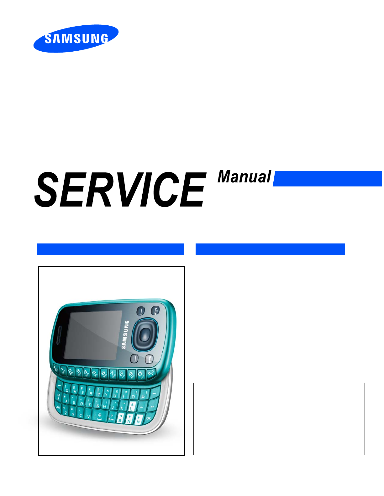
GT-B3310i
GSM TELEPHONE
CONTENTS
Safety Precautions
1.
Specification
2.
Product Function
3.
Exploded View and Parts list
4.
MAIN Electrical Parts List
5.
Level1Repair
6.
Disassembly and Assembly
7.
Instructions
Chart of Troubleshooting
8.
Reference data
9.
Notice
All functionality, features, specifications and other
product information provided in this document inclu
ding, but not limited to, the benefits, design, pricing,
components, performance, availability, and capabiliti
es of the product are subject to change without
-
notice or obligation. Samsung reserves the right to
make changes to this document and the product
described herein, at anytime, without obligation on
Samsung to provide notification of such change.
:
Page 2

Safety Precautions
1.
Repair Precaution
1-1.
Repair in Shield Box, during detailed tuning. Take specially care of tuning or test, because
―
specipicty of cellular phone is sensitive for surrounding interference(RF noise).
Be careful to useakind of magnetic object or tool, because performance of parts is damaged by
―
the influence of magnetic force.
Surely useastandard screwdriver when you disassemble this product, otherwise screw will be
―
worn away.
Useathicken twisted wire when you measure level.
―
thicken twisted wire has low resistance, therefore error of measurement is few.
A
Repair after separate Test Pack and Set because for short danger(for example an overcurrent
―
and furious flames of parts etc) when you repair board in condition of connecting Test Pack and
tuning on.
Take specially care of soldering, because Land of PCB is small and weak in heat.
―
Surely tune on/off while using AC power plug, becausearepair of battery charger is dangerous
―
when tuning ON/OFF PBA and Connector after disassembling charger.
Don't use as you pleases after change other material than replacement registered on SEC System.
―
Otherwise engineer in charge isn't charged with problem that you don't keep this rules.
1-1
SAMSUNG Proprietary-Contents may change without notice
This Document can not be used without Samsung's authorization
Page 3

Safety Precautions
ESD(Electrostatically Sensitive Devices) Precaution
1-2.
Several semiconductor may be damaged easily by static electricity. Such parts are called by ESD
Electrostatically Sensitive Devices), for example IC,BGA chip etc. Read Precaution below.
(
You can prevent from ESD damage by static electricity.
Remove static electricity remained your body before you touch semiconductor or parts with
―
semiconductor. There are ways that you touch an earthed place or wear static electricity prevention
string on wrist.
Use earthed soldering steel when you connect or disconnect ESD.
―
Use soldering removing tool to break static electricity.,otherwise ESD will be damaged by static
―
electricity.
Don't unpack until you set up ESD on product. Because most of ESD are packed by box and
―
aluminum plate to have conductive power,they are prevented from static electricity.
You must maintain electric contact between ESD and place due to be set up until ESD is
―
connected completely to the proper place oracircuit board.
1-2
SAMSUNG Proprietary-Contents may change without notice
This Document can not be used without Samsung's authorization
Page 4
Specification
2.
GSM General Specification
2-1.
GSM850 EGSM900 DCS1800 PCS1900
Freq. Band[MHz]
Uplink/Downlink
ARFCN range 128-251
Tx/Rx spacing 45MHz 45MHz 95MHz 80 MHz
Mod. Bit rate
/BitPeriod
Time Slot Period
/ Frame Period
Modulation 0.3GMSK 0.3GMSK 0.3GMSK 0.3GMSK
824-849
869-894
270.833kbps
3.692us
576.9us
4.615ms
880~915
925~960
0~124 &
975~1023
270.833kbps
3.692us
576.9us
4.615ms
1710~1785
1805~1880
512~885 512~810
270.833kbps
3.692us
576.9us
4.615ms
1850~1910
1930~1990
270.833kbps
3.692 us
576.9 us
4.615 ms
MS Power 33dBm~5dBm 33dBm~5dBm 30dBm~0dBm 30dBm~0dBm
Po w er C la s s 5~19(
Sensitivity -102dBm -102dBm -100dBm -100dBm
TDMAMux8888
Cell Radius 35Km 35Km 2Km 2 Km
SAMSUNG Proprietary-Contents may change without notice
class
4) 5~19(
This Document can not be used without Samsung's authorization
2-1
class
4) 0~15(
class1)
0~15(
class1)
Page 5
Specification
GSM TX power class
2-2.
TX Power
control level
533±2
631±2
729±2
827±2
925±2
10 23±2
11 21±2
GSM850 GSM900
dBm
dBm
dBm
dBm
dBm
dBm
dBm
33±2
31±2
29±2
27±2
25±2
23±2
21±2
dBm
dBm
dBm
dBm
dBm
dBm
dBm
TX Power
control level
030±3
128±3
226±3
324±3
422±3
520±3
618±3
DCS1800 PCS1900
dBm
dBm
dBm
dBm
dBm
dBm
dBm
30±3
28±3
26±3
24±3
22±3
20±3
18±3
dBm
dBm
dBm
dBm
dBm
dBm
dBm
12 19±2
13 17±2
14 15±2
15 13±2
16 11±3
17 9±3
18 7±3
19 5±3
dBm
dBm
dBm
dBm
dBm
dBm
dBm
dBm
19±2
17±2
15±2
13±2
11±3
9±3
7±3
5±3
dBm
dBm
dBm
dBm
dBm
dBm
dBm
dBm
716±3
814±3
912±4
10 10±4
11 8±4
12 6±4
13 4±4
14 2±5
dBm
dBm
dBm
dBm
dBm
dBm
dBm
dBm
16±3
14±3
12±4
10±4
8±4
6±4
4±4
2±5
dBm
dBm
dBm
dBm
dBm
dBm
dBm
dBm
15 0±5
2-2
SAMSUNG Proprietary-Contents may change without notice
This Document can not be used without Samsung's authorization
dBm
0±5
dBm
Page 6

Operation Instruction and Installation
3.
Main Function
Quad Band(GSM850+EGSM900+DCS1800+PCS1900)
-
GPRS Rx/Tx, EDGE Rx only
-
FM Radio
-
Bluetooth v2.0+EDR
-
CSTN
-
CMOS Camera
-2M
MP3 Player
-
2.0"
QVGA
262K
Color LCD
3-1
SAMSUNG Proprietary-Contents may change without notice
This Document can not be used without Samsung's authorization
Page 7
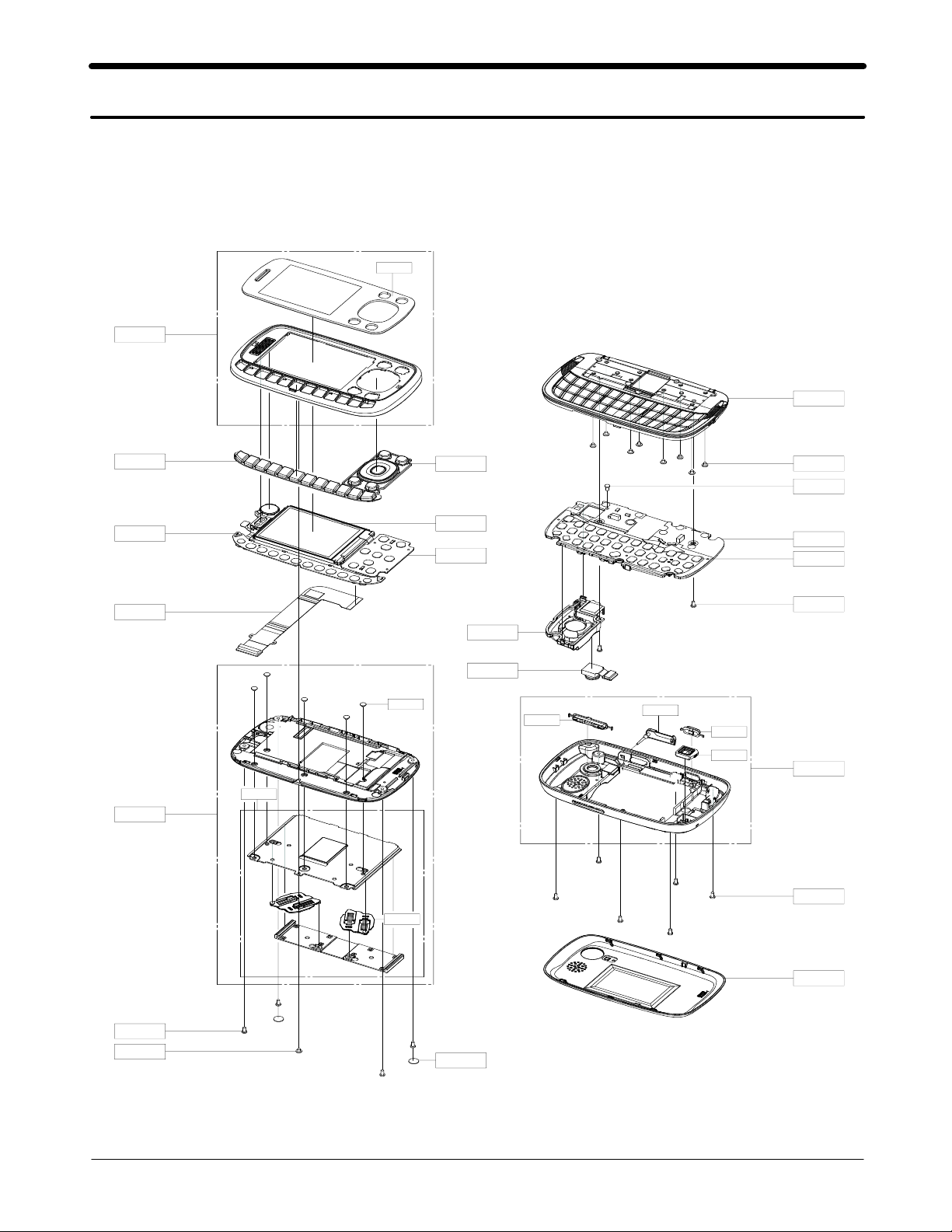
Exploded View and Parts List
4.
Cellular phone Exploded View
4-1.
QMW02
QFU0 1
QFR01
QKP01
QME04
QME16
QFL01
QHI01
QCR93
QHI02
QKP02
QLC01
QLC02
QSP0 1
QCA0 1
QVO01
QCR61
QCR03
QMP01
QME01
QCR03
QRF06
QCK01
QMI03
QRE01
QCR03
QCR03
QCR61
QBA00
QSC01
4-1
SAMSUNG Proprietary-Contents may change without notice
This Document can not be used without Samsung's authorization
Page 8

Exploded View and Parts List
Cellular phone Parts list
4-2.
Design LOC Description SEC CODE
QCR03 SCREW-MACHINE
QCR03 SCREW-MACHINE
QCR03 SCREW-MACHINE
QCR61 SCREW-MACHINE
6001-001811
6001-001811
6001-001811
6001-002008
QME16 ASSY ETC-GTB3310_CON TO CON GH59-07898A
QME01 DOME SHEET-GTB3310_QWERTY
KEY GH59-07899A
35
QCA01 CAMERA MODULE GH59-10284A
QSP01 MODULE-GTB3310I_SPK GH59-10286A
QLC02 ASSY ETC-LCD SUB PBA(GTB3310I) GH59-10372A
QME04 KEY FPCB-TF KEY PBA(GT_B3310I) GH59-10373A
QSC01 TAPE-SCREW CAP GH74-44933C
QMP01 A/S ASSY-GTB3310I_PBA MAIN(SVC) GH82-05326A
QLC01 ELA MODULE-LCD
QVGA GT-B3310 TN ASS GH96-03890A
2.0"
QBA00 ASSY COVER-BATT GH98-13409A
QKP01 ASSY KEYPAD-NUM/TA GH98-13413C
QKP02 ASSY KEYPAD-NAVI/TA GH98-13414C
QFR01 ASSY CASE-FRONT GH98-18838C
QFU01 ASSY CASE-SLIDE UPPER GH98-13405C
QMW02 PMO WINDOW-MAIN(OPEN/TA) GH72-54282C
QFL01 ASSY CASE-SLIDE LOWER GH98-13406C
QCR93 SCREW-MACHINE
6001-002263
QHI01 ASSY HINGE-SLIDE(GTB3310) GH98-13412C
QRE01 ASSY CASE-REAR VE(TA) GH98-18667C
QRF06 PMO COVER-USB GH72-54273A
QVO01 PMO KEY-VOLUME_VE GH72-57959A
QCK01 PMO KEY-CAM_VE GH72-57960A
QMI03 RMO RUBBER-MIC HOLDER GH73-13024A
4-2
SAMSUNG Proprietary-Contents may change without notice
This Document can not be used without Samsung's authorization
Page 9

MAIN Electrical Parts List
5.
SEC CODE Design LOC Description
0403-001741
0404-001172
0406-001167
0406-001267
0406-001286
0406-001369
0501-002606
0502-001322
0504-001140
0505-001165
0505-002388
0601-002070
0601-002268
1001-001488
ZD301 DIODE-ZENER
ZD304 DIODE-SCHOTTKY
ZD303 DIODE-TVS
ZD302,ZD305,ZD306 DIODE-TVS
ZD500,ZD501 DIODE-TVS
U301 DIODE-TVS
Q300 TR-SMALL SIGNAL
Q301 TR-POWER
Q302,Q303 TR-DIGITAL
Q305 FET-SILICON
Q400 FET-SILICON
LED403 LED
LED400,LED401,LED402 LED
U303 IC-ANALOG SWITCH
1001-001598
1009-001035
1108-000355
1201-002944
1201-003025
1203-005851
1203-006098
1205-003517
1205-003998
1205-004030
1404-001224
1405-001231
1405-001298
2007-000138
2007-000138
2007-000140
2007-000141
2007-000143
2007-000143
2007-000144
2007-000146
U302 IC-ANALOG MULTIPLEX
U300 IC-HALL EFFECT S/W
UME200 MEMORY
U101 IC-RF AMP
PAM100 IC-POWER AMP
U403,U404 IC-MULTI REG
U402 IC-MULTI REG
U100 IC-BLUETOOTH
U500 IC-EXPANDER
UCP200 IC-MODEM
TH200 THERMISTOR
R319 VARISTOR
V300 VARISTOR
L303,R107,R108,R110 R-CHIP
R111,R305,R326,R401 R-CHIP
R109,R314 R-CHIP
R410,R411,R500,R501 R-CHIP
R213,R315,R322,R403 R-CHIP
R420,R421,R422,R423 R-CHIP
R416 R-CHIP
R200 R-CHIP
5-1
SAMSUNG Proprietary-Contents may change without notice
This Document can not be used without Samsung's authorization
Page 10

Main Electrical Parts List
SEC CODE Design LOC Description
2007-000148
2007-000148
2007-000148
2007-000157
2007-000162
2007-000162
2007-000168
2007-000170
2007-000172
2007-000242
2007-000831
2007-000932
2007-001119
2007-001284
2007-001288
2007-001292
2007-001307
2007-001316
2007-001339
2007-003015
2007-007001
2007-007015
2007-007142
2007-007488
2007-008780
2203-000233
2203-000254
2203-000278
2203-000386
2203-000438
2203-000585
2203-000627
2203-000643
2203-000679
2203-000812
2203-000812
C405,R309,R311,R312 R-CHIP
R313,R316,R317,R318 R-CHIP
R502,R503 R-CHIP
R400,R419 R-CHIP
R116,R205,R206,R209 R-CHIP
R302,R321 R-CHIP
R310 R-CHIP
R404 R-CHIP
R303,R304 R-CHIP
R308,R324,R325 R-CHIP
R306 R-CHIP
R301 R-CHIP
R323 R-CHIP
R408,R409 R-CHIP
R412,R413,R414,R415 R-CHIP
R327,R328 R-CHIP
R115 R-CHIP
R113,R114 R-CHIP
R402 R-CHIP
R105 R-CHIP
R300 R-CHIP
R320 R-CHIP
R204 R-CHIP
R405 R-CHIP
R307 R-CHIP
C233 C-CERAMIC
C107,C118 C-CERAMIC
C103 C-CERAMIC
C106,C305,C306 C-CERAMIC
C124,C207,C210 C-CERAMIC
C326,C327 C-CERAMIC
C222,C223 C-CERAMIC
C100 C-CERAMIC
C328 C-CERAMIC
C117,C309,C310,C315 C-CERAMIC
C318,C319,C323,C403 C-CERAMIC
5-2
SAMSUNG Proprietary-Contents may change without notice
This Document can not be used without Samsung's authorization
Page 11
Main Electrical Parts List
SEC CODE Design LOC Description
2203-000812
2203-000995
2203-001153
2203-001385
2203-002443
2203-002487
2203-002668
2203-002677
2203-002709
2203-005234
2203-005281
2203-005344
2203-005480
2203-005481
2203-005483
2203-005552
2203-005968
2203-006048
2203-006048
2203-006048
2203-006048
2203-006190
2203-006201
2203-006257
2203-006260
2203-006324
2203-006361
2203-006399
2203-006399
2203-006399
2203-006562
2203-006562
2203-006872
2203-007240
2203-007270
2203-007271
C404 C-CERAMIC
C302,C311 C-CERAMIC
C324,C325 C-CERAMIC
C131 C-CERAMIC
C119,C120,C225 C-CERAMIC
C220,C228 C-CERAMIC
C135,C226 C-CERAMIC
C134 C-CERAMIC
C218 C-CERAMIC
C116,C126 C-CERAMIC
C114 C-CERAMIC
C303 C-CERAMIC
C221 C-CERAMIC
C122,C123,C203,C219 C-CERAMIC
C313,C314 C-CERAMIC
C111 C-CERAMIC
C234 C-CERAMIC
C101,C105,C200,C201 C-CERAMIC
C205,C209,C213,C224 C-CERAMIC
C231,C300,C301,C321 C-CERAMIC
C322 C-CERAMIC
C202 C-CERAMIC
C110 C-CERAMIC
C208,C214,C308 C-CERAMIC
C211,C229,C230 C-CERAMIC
C217 C-CERAMIC
C331,C334 C-CERAMIC
C121,C204,C212,C232 C-CERAMIC
C235,C304,C312,C316 C-CERAMIC
C401,C402,C413,C500 C-CERAMIC
C215,C400,C414,C415 C-CERAMIC
C416,C417,C418,C419 C-CERAMIC
C109 C-CERAMIC
C227,C317 C-CERAMIC
C206 C-CERAMIC
C216,C406,C407,C408 C-CERAMIC
5-3
SAMSUNG Proprietary-Contents may change without notice
This Document can not be used without Samsung's authorization
Page 12

Main Electrical Parts List
SEC CODE Design LOC Description
2203-007271
2203-007279
2203-007290
2409-001172
2703-000213
2703-001747
2703-001749
2703-001749
2703-001750
2703-001838
2703-001990
2703-002199
2703-002203
2703-002204
2703-002369
2703-003869
2801-004896
2801-004902
2901-001408
2904-001923
2904-001924
3003-001136
3301-001342
3301-001729
3301-001812
3301-001986
3301-002000
3404-001303
3705-001731
3709-001627
3709-001630
3711-006105
3711-006919
C409,TA302 C-CERAMIC
C102 C-CERAMIC
C113 C-CERAMIC
BAT200 CAPACITOR
L120 INDUCTOR-SMD
L122 INDUCTOR-SMD
L108,L110,L114,L115 INDUCTOR-SMD
L116,L118,L123,L124 INDUCTOR-SMD
L104,L105 INDUCTOR-SMD
L301 INDUCTOR-SMD
L113 INDUCTOR-SMD
L109,L112 INDUCTOR-SMD
L101 INDUCTOR-SMD
L107 INDUCTOR-SMD
L106 INDUCTOR-SMD
L201 INDUCTOR-SMD
OSC201 CRYSTAL-UNIT
OSC200 CRYSTAL-UNIT
F400,F401,F402 FILTER-EMI SMD
F102 FILTER-SAW
F101 FILTER-SAW
MIC300 MIC-CONDENSOR
F300 CORE-FERRITE BEAD
L305 CORE-FERRITE BEAD
L307,L308 CORE-FERRITE BEAD
L302,L304 CORE-FERRITE BEAD
L200 CORE-FERRITE BEAD
TAC400,TAC401,TAC402 SWITCH-TACT
RFS100 CONNECTOR-COAXIAL
SIM300 CONNECTOR-CARD EDGE
U501 CONNECTOR-CARD EDGE
HEA400 CONNECTOR-HEADER
HEA401 CONNECTOR-HEADER
3711-006137
3712-001348
3712-001363
BTC300 HEADER-BATTERY
ANT100,ANT101 CONNECTOR
ANT102,ANT103 CONNECTOR
5-4
SAMSUNG Proprietary-Contents may change without notice
This Document can not be used without Samsung's authorization
Page 13

Main Electrical Parts List
SEC CODE Design LOC Description
3722-002840
4709-001615
IFC300 JACK-PHONE
F100 RF-MODULE
GH70-03349A SC101,SC103,SC105 IPR SHIELD-CAN CLIP
GH70-04828A SC100,SC102,SC104 IPR SHIELD-CAN CLIP
Please consult the GSPN website(Samsung Portal) for the most recent version of the product's
part list.
5-5
SAMSUNG Proprietary-Contents may change without notice
This Document can not be used without Samsung's authorization
Page 14
Array course control
6.
S/W Download
6-1.
6-1-1.
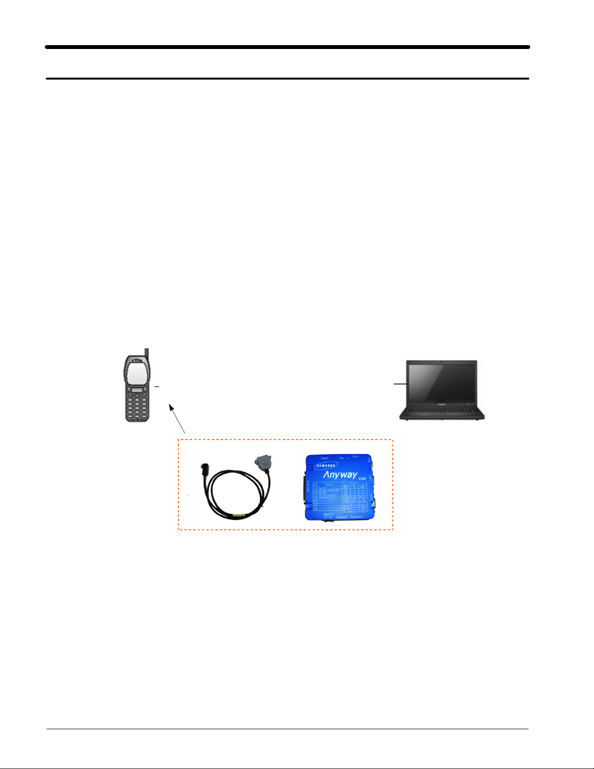
Pre-requsite for S/W Downloading
Downloader Program(
•
GT-E1170 Mobile Phone
•
Data Cable
•
JIG BOX(GH99-36900A)
•
RF Test Cable(GH39-00985A)
•
JIG Cable(GH39-01290A)
•
Adapter(GH99-38251A)
•
Serial Cable
•
Binary files
•
Settings
(
Connect to ANYWAY JIG BOX
FlashTool_E2_ROU")
"
JIG CABLE(Phone to JIG)
&
6-1
SAMSUNG Proprietary-Contents may change without notice
This Document can not be used without Samsung's authorization
Page 15
Array course control
6-1-2.
S/W Downloader Program
Load the binary download program by executing the
.
1
FlashTool_E2.exe"
"
6-2
SAMSUNG Proprietary-Contents may change without notice
This Document can not be used without Samsung's authorization
Page 16
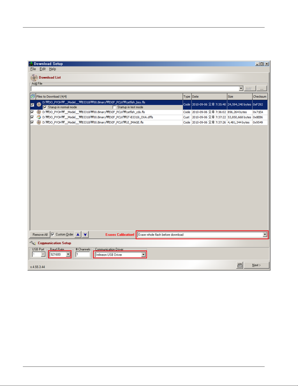
Array course control
Select the
.
2
Communication Driver/Baud rate/Download-setup
mobile phone is connected to
that the
.
.
6-3
SAMSUNG Proprietary-Contents may change without notice
This Document can not be used without Samsung's authorization
Page 17
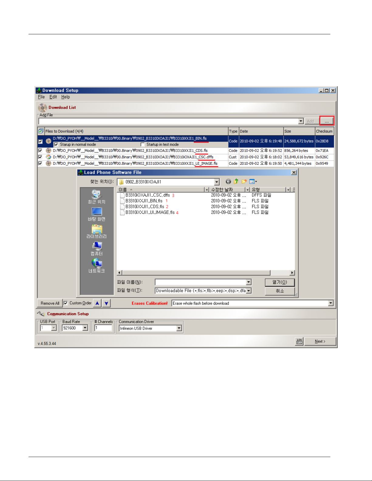
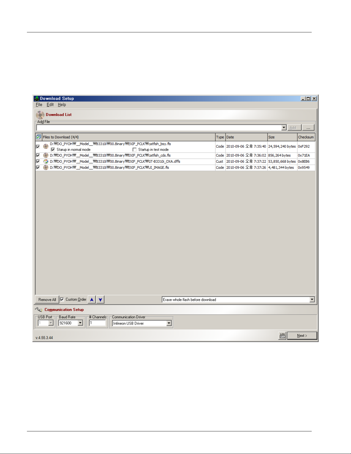
Array course control
Select the Download file
.
3
Caution:Keep order of files
*
(*.
fls
dffs-total4file)
,*.
6-4
SAMSUNG Proprietary-Contents may change without notice
This Document can not be used without Samsung's authorization
Page 18
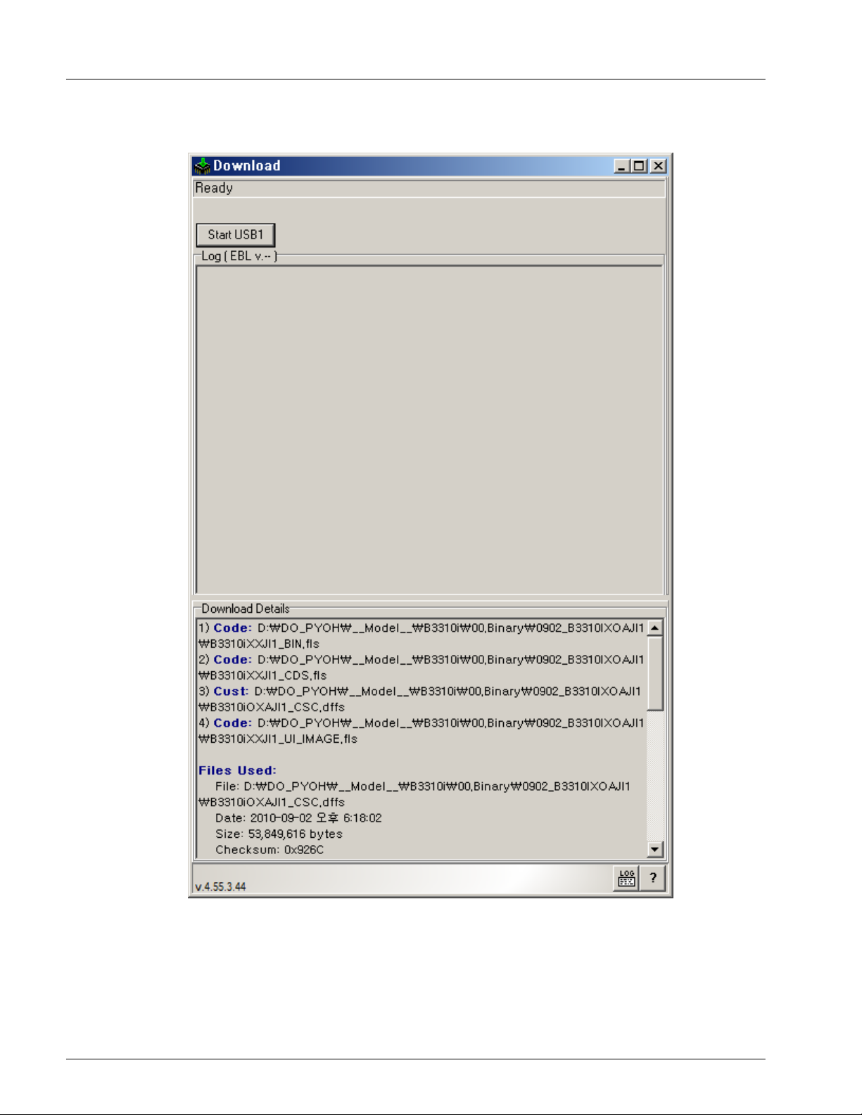
Array course control
4
.
Click
Start'
'
Button.
6-5
SAMSUNG Proprietary-Contents may change without notice
This Document can not be used without Samsung's authorization
Page 19
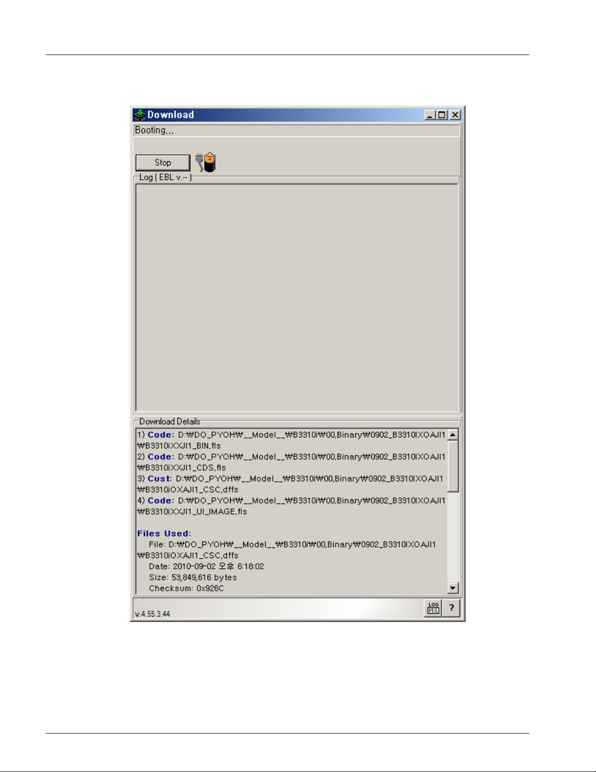
Array course control
. Click'Start USB1'.And connect phone(without battery) by USB DATA cable.
5
Insert battery to phone. Download is starting.
.
6
Confirm the downloaded version name and etc.
.
7
*#1234#
Full Reset
:
*2767*3855#
6-6
SAMSUNG Proprietary-Contents may change without notice
This Document can not be used without Samsung's authorization
:
Page 20
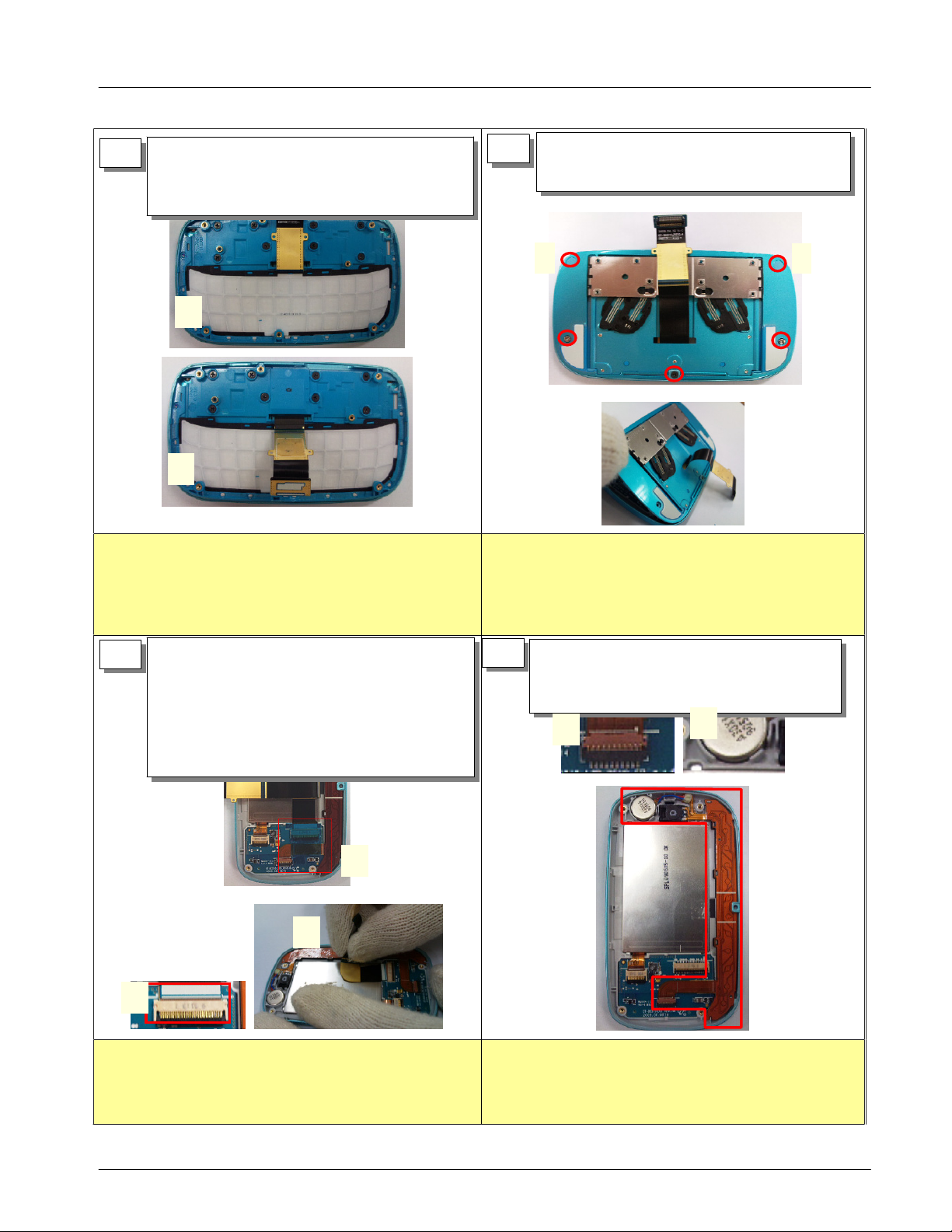
Disassembly and Assembly Instructions
7.
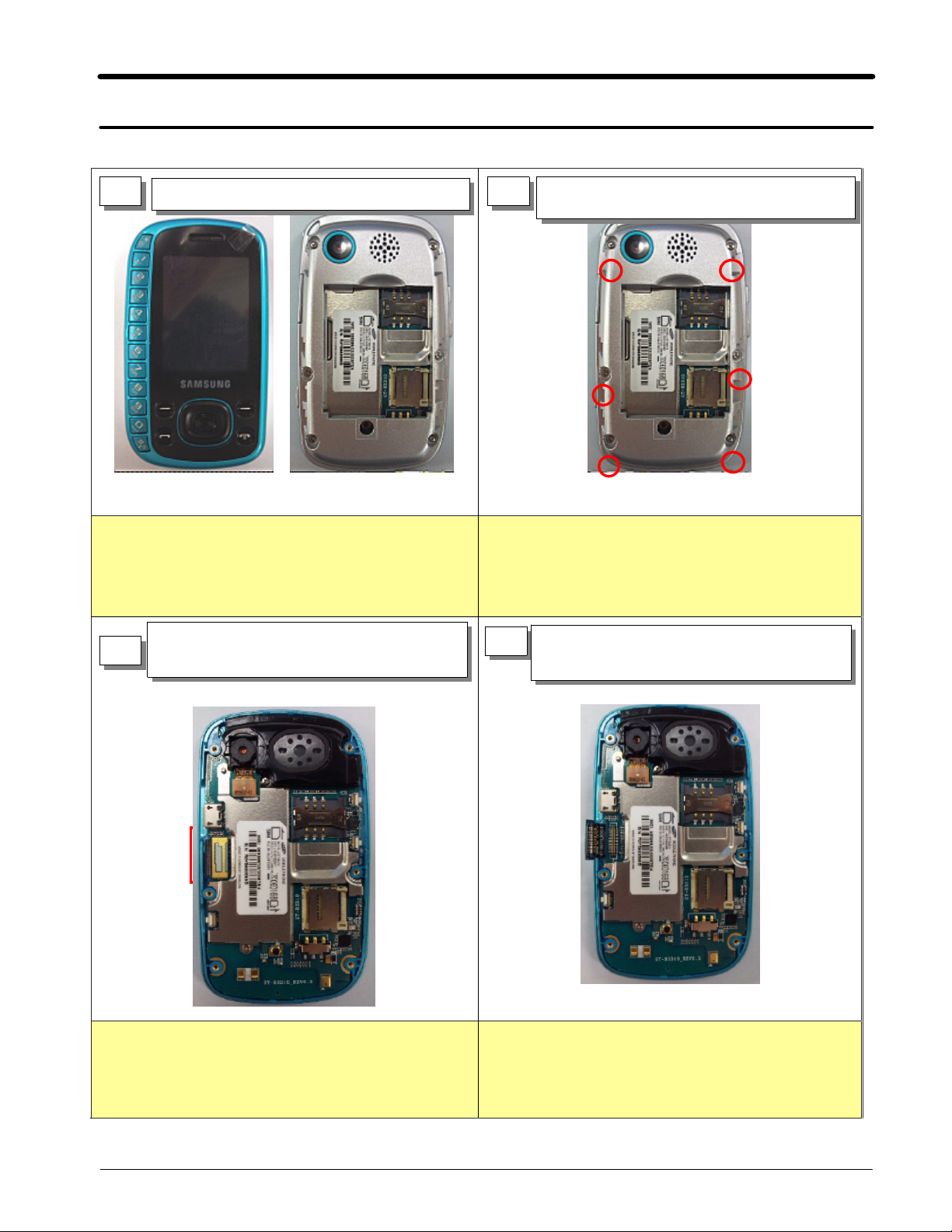
Disassembly
7-1.
1
Be careful not to occur any damages and scratches
1)
Remove the battery cover and the battery
1)
.
2
Be careful not to occur any damages and scratches.
1)
Be careful not to change shape of the REAR during
2)
disassembly.
Unscrew6screw points.
1)
Unlock the set from the top to the bottom.
2)
Remove the Slide FPCB Connector from
1)
3
the the board.
Be careful not to occur any damages to the slide
1)
FPCB
.
4
Unscrew the1point below the speaker.
1)
Unscrew the1point beside the RF S/W.
2)
①
②
Be careful not to occur any damages to components
1)
around screws during disassembly.
7-1
SAMSUNG Proprietary-Contents may change without notice
This Document can not be used without Samsung's authorization
Page 21
Disassembly and Assembly Instructions
5
Take apart the Slide FPCB to the
1)
Front.(Double Sided tape)
Unscrew8screw points.
2)
Remove the screw caps,
1)
6
Unscrew8screw points.
2)
Take apart the Lower
3)
①~②
①
②
Be careful not to occur damages to the SLIDE FPCB.
1)
Be careful not to occur any damages to parts of the
2)
FRONT and the FPCB during disassembly.
Remove the friction tape which holds the LCD
1)
7
FPCB.
Open the FPCB actuator.
2)
Remove the Main Slide FPCB carefully.
3)
Notice that there isadouble sided friction tape at
(
the bottom.
①
Be careful not to occur any damages and scratches
1)
Be careful not to occur any damages to parts of the
2)
②
Lower and the FPCB during disassembly.
8
Remove the NUM KEY FPCB actuator.
1)
Disassemble the whole after removing the motor
2)
by tweezers
①
②
.
①
③
②
Remove with rounded tweezers.
1)
Be careful not to occur any damages and scratches
2)
to FPCB(It could be torn.)
SAMSUNG Proprietary-Contents may change without notice
This Document can not be used without Samsung's authorization
Remove with rounded tweezers.
1)
Be careful not to occur any damages and scratches
2)
to the FPCB.
7-2
Page 22
Disassembly and Assembly Instructions
9
Remove the NUM Keypad
1)
Open the LCD FPCB actuator.
2)
Remove the LCD connector carefully.
3)
①
②
Be careful not to occur any damages and scratches
1)
to the LCD
Take apart the SUB PBA to the UPPER.
1)
10
It is easy to remove the SUB PBA when
push it from the SUB KEYPAD side.
Be careful the bending on SUB PBA during the
1)
removing.
Be careful not to occur any damages and scratches.
2)
11
Be careful not to occur any damages and scratches.
1)
Remove the SUB Key PAD.
1)
7-3
SAMSUNG Proprietary-Contents may change without notice
This Document can not be used without Samsung's authorization
Page 23

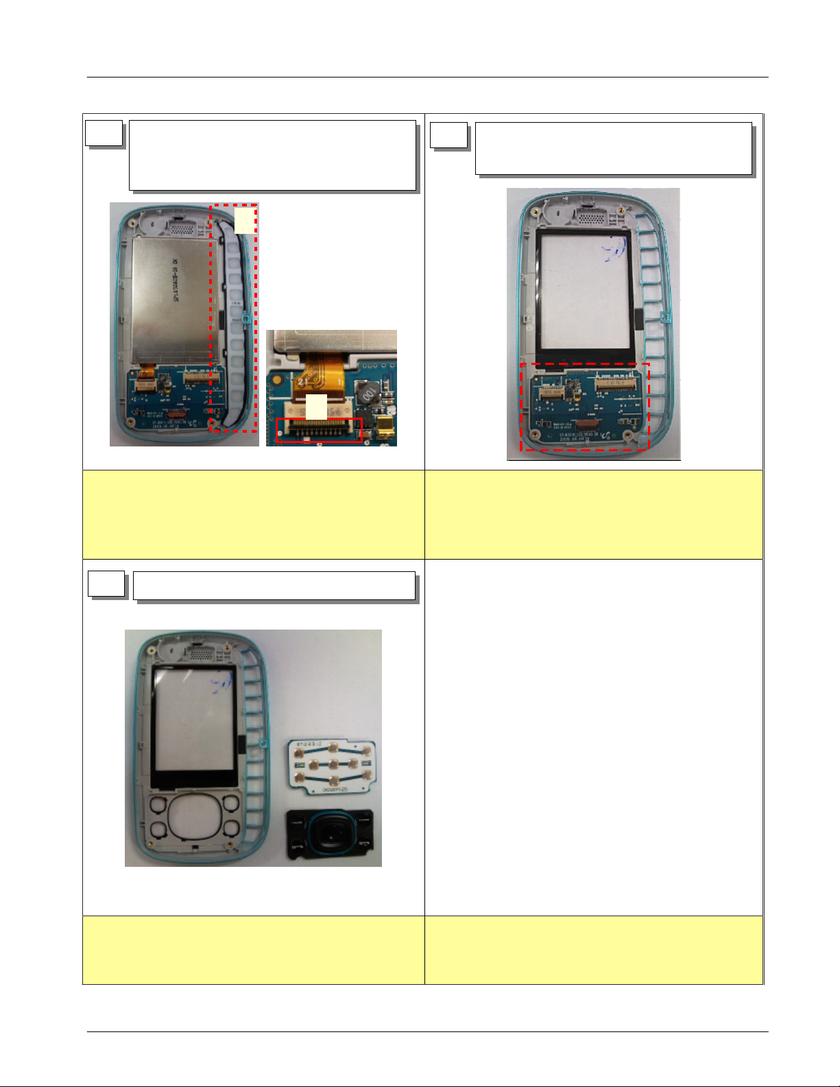
Disassembly and Assembly Instructions
1 2
Be careful dirt on the window.
1)
Be careful not to occur any damages and scratches
2)
Put the SUB Keypad on the Slide Upper.
1)
Assemble the LCD FPCB to the Sub PBA.
2)
on LCD.
Be careful not to occur any damages to components
3)
on SUB PBA.
Put the LCD on the grooves at the top side of
1)
the SLIDE UPPER.
Put the SUB PBA
2)
Put the NUM Keypad.
3)
①
③
②
Be careful to damage to the LCD and dirts on
1)
window during assembly
Assemble components on SUB PBA carefully
2)
Connect the NUM KEY FPCB to the SUB PBA
1)
3
Connector.
Put the NUM Key keep away from the screw holes
2)
Put the MOTOR/Receiver FPCB.(Line cleanup)
3)
Be careful not to occur any damages to the FPCB.
1)
Pay attention to handle the lines after placing the
2)
MOTOR/RECEIVER.
Assemble the SLIDE FPCB according to
1)
4
baselines
Confirm the baselines.
2)
Fold the bottom of FBCB's folding part to the
3)
other side and lift it up.
①
Be careful to occur any damages and scratches on
1)
the FPCB.
7-4
SAMSUNG Proprietary-Contents may change without notice
This Document can not be used without Samsung's authorization
Page 24

Disassembly and Assembly Instructions
7 8
Confirm the baselines of all connectors
1)
Put the SUB PBA friction tape.
2)
①
②
Put them follow the baselines.
1)
Lift the hinge and put the lower on.
1)
Pay attention to the screw hole during the
assembly.
Be careful to occur any damages and scratches to
1)
the injections
Be careful to occur any damages and scratches on
1)
the FPCB.
7
Use appropriate screws.
1)
Be careful not to occur any damages to the injection
2)
Screw the5screw point.
1)
Torque
-
Size
-
Torque
-
Size
-
:1.0~1.2
: M1.4*
:0.8~1.0
: M1.4*
L3.0
L1.7
Kgf·cm
Kgf·cm
during screwing.
Through the SLIDE FPCB into the groove
1)
8
of the FRONT.
①
Be careful not to occur any damages and scratches
1)
to the FPCB.
7-5
SAMSUNG Proprietary-Contents may change without notice
This Document can not be used without Samsung's authorization
Page 25

Disassembly and Assembly Instructions
Screw the8screw points.
1)
Put the SLIDE FPCB on the FRONT.
2)
Double sided tape)
(
Torque
-
Size
-
Be careful not to occur any damages to the injection
1)
:0.8~1.0
: M1.4*
Kgf·cm
L1.7
during screwing.
Put the SLIDE FPCB appropriately follow left/right
2)
grooves.
1091)
Put the PBA on and connect the SLIDE
FPCB Connector.
Screw the right side of the CAMERA and
2)
left side of the RF SW.
Torque
-
Size
-
Be careful not to occur any damages to the FPCB.
1)
Be careful not to occur any damages to components
2)
:1.0~1.2
: M1.4*
Kgf·cm
L3.0
around screw points during screwing.
11
Be careful not to occur any damages to the injection
1)
Assemble the REAR
1)
Screw6screw points.
2)
Torque
-
-
Size
:1.0~1.2
: M1.4*
Kgf·cm
L3.0
during the screwing.
Confirm the appearance and functions.
1)
12
Check the appearance.
1)
7-6
SAMSUNG Proprietary-Contents may change without notice
This Document can not be used without Samsung's authorization
Page 26

Level
8.
Block Diagram
8-1.
Repair
3
m
h
W
W
O
m
6
0
1
3
x
x
2
2
W
m
m
h
m
m
h
O
O
0
0
0
0
6
8
1
7
1
1
2
2
1
P
L
R
S
S
H
H
e
n
o
h
l
a
p
t
i
o
r
g
i
c
i
D
M
t
n
)
e
D
m
/
e
A
r
(
u
F
I
s
a
e
M
d
a
p
y
e
K
F
I
C
M
I
s
S
u
b
t
i
b
2
C
3
M
M
/
D
S
s
u
b
t
i
b
-
F
l
I
4
a
-
6
n
y
r
r
e
o
t
x
m
E
e
M
t
e
o
s
e
d
r
a
e
e
t
S
H
o
i
d
a
r
M
F
C
C
D
0
.
2
S
B
F
S
U
F
I
S
U
M
S
G
6
7
1
1
M
R
A
N
P
P
P
P
S
E
E
L
e
r
c
e
e
i
k
p
d
a
r
e
u
a
p
o
E
s
L
U
T
P
G
y
e
r
t
o
i
L
m
e
K
M
A
E
-
T
R
I
r
e
M
h
S
p
i
G
C
M
O
R
M
A
R
e
h
c
a
c
P
C
N
I
S
L
M
I
A
D
/
S
²
I
l
o
r
t
F
n
R
o
C
c
i
s
M
K
S
M
G
C
A
D
N
N
C
C
C
I
I
I
M
M
M
X
c
i
U
M
M
C
A
M
N
M
A
V
V
X
U
U
M
A
P
L
L
C
M
I
T
S
R
L
L
F
I
L
D
L
S
P
C
I
C
M
I
U
M
V
V
p
n
y
l
m
o
i
p
u
t
p
a
P
u
r
S
e
e
n
c
g
i
r
e
a
g
M
h
C
B
S
U
V
r
o
t
a
r
b
i
V
e
r
o
c
V
P
S
D
C
D
A
z
H
k
2
3
w
o
L
V
m
0
0
6
r
…
o
V
f
)
m
t
e
5
3
g
u
1
o
a
t
l
VCHG
o
o
i
d
v
V
u
e
5
.
a
v
2
i
~
t
r
a
a
l
g
VS H N T
o
e
p
i
n
b
(
V
8
.
1
max.1.5mA
VD D C H G
CSB
e
g
r
a
h
C
C
D
/
C
D
k
c
a
B
U
M
P
F
R
O
X
r
e
w
o
P
…
V
V
8
0
,
.
1
1
CS
SE NS EP
SE NS EN
k
c
VB AT 2
u
B
t
h
g
i
l
O
X
C
D
F
n
0
0
1
,
s
p
a
c
g
n
i
k
c
o
l
b
O
D
L
3
k
4
A
μ
5
.
7
4
2
1
hfe>200
F
μ
0
1
V
0
2
…
V
5
.
4
E
G
R
A
H
C
V
k
7
2
1
7
k
4
5
3
S
7
4
8
C
B
6
.
n
i
m
r
0
7
e
4
g
r
a
e
h
l
0
1
p
2
T
C
0
m
5
a
2
x
y
e
r
P
r
T
e
o
X
t
f
t
Z
a
B
%
5
5
1
.
0
)
V
6
(
V
1
.
5
…
V
5
0
.
3
)
V
0
(
C
D
/
C
D
A
P
M
E
F
8-1
SAMSUNG Proprietary-Contents may change without notice
This Document can not be used without Samsung's authorization
Page 27

Level3Repair
PCB Diagrams
8-2.
8-2-1.
Top
R
2
1
3
BAT200
C
2
2
9
G100
HEA401
MEM_INT
R
R
R
C413
2
2
R
3
3
5
Q
0
I
F
C
3
0
0
C
4
0
4
A
C
4
0
1
1
0
3
0
R
3
U
3
0
4
0
R
3
1
R
5
0
3
R
4
0
0
R
R
C
4
4
4
0
0
0
9
8
3
F
4
1
0
0
2
2
3
0
1
2
C
2
1
0
6
7
0
4
A
E
H
T
1
0
4
D
Z
1
G
2
2
C
C
2
1
0
C
2
3
1
F
4
0
1
8
2
2
C
F
C
2
4
0
5
0
0
C
2
1
4
C401
2
0
C
4
R
3
2
4
0
0
4
C
C418
4
R
0
4
0
3
4
C419
U
L119
4
8
1
1
1
1
L
L
C135
C127C128
L115L116
0
3
9
2
C
C
1
1
3
4
4
0
1
0
1
1
1
1
7
0
1
4
4
C
C
4
3
1
Q
0
3
3
C
3
0
3
C
R321
3
0
3
U
TP_ADVn
R326
1
0
R
3
R300
0
0
5
CS_RAM
Q300
U
TP_UBU
R
R
C
R
5
5
5
5
0
0
0
0
1
2
0
0
RST_BB
TP_WEn
R
4
C
2
L
6
0
2
C
C
2
3
0
0
8
2
1
1
L
0
1
1
L
0
0
1
T
N
A
0
0
1
2
2
C
C223
C
0
2
7
1
1
2
C
2
C
0
0
2
C
2
2
C
R
4
S
2
0
O
7
7
1
C
4
L113
9
0
1
L
L111
F101F102
0
1
1
R
8
0
1
L
0
0
L102
L
1
2
4
C100
L101
L121
1
0
1
T
N
A
SC101
T
P
4
3
C
2
_
R
C233
C412
TP_AD_ZERO
D
n
2
0
E
0
M
U
C224
C235
C201
C211
T
R
H
2
2
0
0
4
0
2
P
C
C222
R
8
1
0
1
1
1
R
1
M
A
O
U
S
C
2
0
1
6
0
R
2
5
0
R
2
C204
3
0
C
2
C202
9
1
C
2
C215
0
2
C
2
C
R
R
1
0
9
P
2
1
1
0
1
0
7
7
1
C
3
0
C
1
C101
4
0
1
5
L
0
1
L
6
0
1
L
C116
2
2
1
L
1
3
C
1
2
3
1
C
5
1
C
1
C209
R
2
0
0
1
0
2
R
CS_NOR
TP_MEMCLK
3
0
1
C
S
TP_LBU
C
2
1
2
3
1
2
C
9
0
R
3
R310 R311
S
C
1
0
0
5
0
1
C
S
5
1
R
3
R314
C308
C323
SIM300
8
0
C
2
SC104
U
5
0
1
SC102
T
B
3
0
C
R
3
0
RFS100
C
R
1
1
3
0
4
4
0
0
R
1
L
1
0
0
5
0
0
3
V
R102
R101
6
3
1
1
3
3
C
C
0
L
5
3
9
4
1
0
1
1
3
5
3
3
C
R
C
1
1
C
3
C
0
1
3
9
0
C
3
ZD400
TAC400
0
0
5
Z
D
ZD501
TAC402
0
0
2
N
C
G102
C
3
1
2
R
2
1
3
R313
ZD303
C
1
1
3
6
2
1
C
C
1
1
1
L123
3
3
1
C
F100
4
7
1
0
1
1
3
0
1
L
L
C
5
0
C
1
8
1
C
6
0
1
C
R
2
0
9
6
1
1
R
Z
D
3
1
0
D
X
R
_
T
B
_
1
0
3
C
P
C331
1
U
C124
1
0
7
0
C
1
0
0
1
1
C
5
0
R
1
C109
D
X
T
_
T
B
_
P
T
T
G103
MIC300
8-2
SAMSUNG Proprietary-Contents may change without notice
This Document can not be used without Samsung's authorization
Page 28

Level3Repair
8-2-1.
Bottom
3
K
0
0
P
S
4
1
4
5
0
N
E
0
H
P
Y
H
_
Q
_
S
H
I
F
Q
_F
N
Z
_
Q
Q
_
X
Q
_
C
Q
_
V
T
Q
_
A
Q
_
S
Q
_
D
Q
_
F
G
_
Q
E
R
T
Q
_
Q
Q
W
_
Q
_
Q
_
Q
_
Q
R
2
0
4
D
E
L
R
4
1
C409
C408
C407
R
3
2
7
C
3
1
9
L
C
R
3
3
3
4
0
2
2
2
7
3
1
8
R
C322
C
C
L
3
3
5
3
0
2
2
2
8
6
3
7
R
C318
TP_UART_RXD_USB
TP_UART_TXD_USB
3
2
0
U
T
R
R
L
A
3
0
2
L
E
D
4
0
3
R
4
1
5
R
3
3
3
3
6
0
1
1
0
0
3
6
7
8
3
R
C
4
3
0
TP_USB_SW_INT
R420
R421
3
0
C416
4
U
C415
C414
9
C
3
0
6
2
R
4
1
6
Z
D
0
3
0
4
U
R
3
2
3
C406
C317
2
0
1
T
N
A
C
6
2
2
C225
C
0
1
0
2
2
1
L
5
C
4
0
5
2
6
0
0
3
C
3
L
5
3
4
2
0
D
0
3
4
3
Z
C325
3
2
1
C
R114
L
C
0
4
Z
3
D
C302
U300
R
3
0
2
Q
3
0
3
F300
C
R
3
0
Q
2
3
3
0
1
0
8
R
3
2
0
5
1
1
R
R
1
1
3
C119
0
1
1
U
L
1
2
0
0
2
1
C
C122
ZD302
1
0
3
8
L
2
3
C
E
C
A
P
S
_
Q
H
_
Q
M
Y
S
_
Q
B
_
Q
N
_
Q
Q
_
M
Q
_
O
K
J
_
Q
K
_
Q
_
Q
L
K
C
A
B
_
Q
R
E
T
N
E
_
Q
Y
U
_
Q
R
4
1
3
1
0
4
D
E
L
I
_
Q
_
Q
O
_
Q
P
_
Q
1
5
N
E
0
H
P
Y
H
_
Q
2
1
4
R
0
0
4
D
E
L
1
3
T
0
N
A
Q400
R402
R
4
0
4
R405
8-3
SAMSUNG Proprietary-Contents may change without notice
This Document can not be used without Samsung's authorization
Page 29

Level3Repair
Flow Chart of Troubleshooting
8-3.
presetting methods for checking TP
※
GND&TP using Oscilloscope
-
look over the coming out signal.
-
GND
Oscilloscope
←
TP(Test Point)
8-4
SAMSUNG Proprietary-Contents may change without notice
This Document can not be used without Samsung's authorization
Page 30

Level3Repair
Multi-meter
←
EX) to look up the TP, shunt Cap.
-
Checking the TP(test point) using Multi-meter
←
if checking the GND, you can listen"beep"
-
if checking the Signal, you can't listen it.
8-5
SAMSUNG Proprietary-Contents may change without notice
This Document can not be used without Samsung's authorization
Page 31

Level3Repair
8-3-1.
Power On
Power on does not work
YES
Battery Voltage
YES
check the current consumption is
check the current consumption is
less than
less than30mA
350
YES
NO
≥
mA
3.3V?
NO
yes
NO
Change the Battery
change the PBA
Download or change the PBA
VDD_2.9V
TP: C214)
(
VDD_1.8V
TP: C218)
(
VDD_CORE_1.2V
Check the oscillator clock
OSC200(C223)
OSC201(pin3)
TP: C211)
(
END
=2.9
=1.8
YES
=32.768
MHz,OK?
=26
YES
V?
V?
=1.2
V?
kHz
NO
NO
,
Re-solder UCP200 or change the PBA
Re-solder or change the
OSC200,OSC201,C223,C222
8-6
SAMSUNG Proprietary-Contents may change without notice
This Document can not be used without Samsung's authorization
Page 32

Level3Repair
VDD_2.9V
VDD_IO1_1.8V
VBAT
VDD_1.8V V_EARMIC_2.2V
VDD_EBU_1.8V
VDD_TRX_1.4V
VMMC_2.85V
V_MIC_2.2V
VBAT
VSIM_2.85V
VUSB_3.1V
VDD_RF2_2.5V
VDD_TDC_1.3V
VDD_TRX_1.4V
VUSB_3.1V
VDD_TDC_1.3V
C203
C222
VDD_1.8V
C228
C226
C227
C204
OSC200
C223
C225
CLOSE TO XO(SHIELD & CUT FILL)
VDD_1.8V
C232
FM_LNA_OUT
OSC201
2
C229
C205
VRTC_2.3V
43
1
R213
1
2
BAT200
C210
C220
SIM_IO
SIM_RST
SIM_CLK
KEY_SLIDE_EN_BB
CAM_MCLK_OUT
MEM_CLK
CLOSE TO THE PIN(0.3T)
CS
CSB
CS0n_NOR
CS1n_RAM
SLIDE_ON
NUM_KEY_EN_BB
USB_DM_BB
USB_DP_BB
RCV_N
RCV_P
SPK_N
SPK_P
LB_RX_P
HB_RX_P
LB_RX_N
HB_RX_N
LB_TX
HB_TX
FM_LNA_SW
UBn
LBn
UART1_RXD
UART1_TXD
UART2_RXD_BT
UART2_TXD_BT
KEY_BL
SENSE_N
SENSE_P
VLOGIC
BS2
ONKEY
RST_BB_J
RST_BB
CLOSE TO THE PIN
C202
ISOLATE
NOISY
L200
L201
BT_RST
C230
C231
VDD_RF2_2.5V
VDD_NEG_1.3V
C211
VDD_IO2_1.8V
VCHG
VDDCHG
C214
C215
C216
C218
C217
ROUTE FROM EACH CAP
AD(0:15)
A(16:23)
CAM(0:7)
CAM_STANDBY
CAM_PCLK_IN
CAM_RST
CAM_HSYNC
LCD(0:7)
R206
R205
CAM_VSYNC
LCD(0)
LCD(1)
LCD(2)
LCD(3)
LCD(4)
LCD(5)
LCD(6)
LCD(7)
EN_CAM_PWR
LCD_RS
USB_I2C_SCL
LCD_DET
LCD_WR
LCD_CS
LCD_RST
KEY_INT
LCD_BL_EN
USB_I2C_SDA
KEY_RST
LCD_ID
KEY_SCL_1.8V
KEY_SDA_1.8V
R204
TH200
CSn_ONENAND
AUX_MIC_N
AUX_MIC_P
SD_DATA(0)
SD_DATA(1)
SD_DATA(2)
SD_DATA(3)
SD_CLK
SD_CMD
PCM_RXD
PCM_TXD
CAM_SCL
CAM_SDA
PCM_SYNC
PCM_CLK
FLM
VF
MIC_N
MIC_P
TCK
TDI
TDO
TMS
AD(0)
AD(1)
AD(2)
AD(3)
AD(4)
AD(5)
AD(6)
AD(7)
AD(8)
AD(9)
AD(10)
AD(11)
AD(12)
AD(13)
AD(14)
AD(15)
CAM(0)
CAM(1)
CAM(2)
CAM(3)
CAM(4)
CAM(5)
CAM(6)
CAM(7)
K3
A|D0
K2
A|D1
L1
A|D2
M1
A|D3
N3
A|D4
M2
A|D5
N1
A|D6
P2
A|D7
K1
A|D8
L4
A|D9
L2
A|D10
L3
A|D11
N2
A|D12
P5
A|D13
P1
A|D14
P3
A|D15
R1
A(16)
A16
J4
A(17)
A17
J2
A(18)
A18
H4
A(19)
A19
P4
A(20)
A20
R2
A(21)
A21
J3
A(22)
A22
T3
A(23)
A23
N4
A24
A6
CIF_D0
B6
CIF_D1
C5
CIF_D2
A7
CIF_D3
B7
CIF_D4
C6
CIF_D5
C7
CIF_D6
E8
CIF_D7
G7
CIF_PD
G6
CIF_PCLK
E6
CIF_RESET
F7
CIF_HSYNC
E7
CIF_VSYNC
E1
DIF_D0
D1
DIF_D1
F2
DIF_D2
D3
DIF_D3
C2
DIF_D4
C1
DIF_D5
B1
DIF_D6
F3
DIF_D7
E2
DIF_D8
E3
DIF_CD
F1
DIF_HD
D4
DIF_RD
G1
DIF_VD
C3
DIF_WR
F4
DIF_CS1
D2
DIF_RESET
A9
KP_IN0
A10
KP_IN1
B10
KP_IN2
C10
KP_IN3
D10
KP_IN4
E10
KP_IN5
D9
KP_OUT0
B9
KP_OUT1
C9
KP_OUT2
E9
KP_OUT3
F10
KP_OUT5
N12
M0
T11
M1
R11
M2
J13
MON1
J12
MON2
C4
MON3
R12
MICN1
R13
MICN2
T12
MICP1
T13
MICP2
H3
MMCI_DAT0
H6
MMCI_DAT1
G5
MMCI_DAT2
K5
MMCI_DAT3
H2
MMCI_CLK
H1
MMCI_CMD
A8
I2S1_RX
B8
I2S1_TX
B5
I2C_SCL
A5
I2C_SDA
C8
I2S1_WA0
D8
I2S1_CLK0
H16
TCK
J16
TDI
J15
TDO
G16
TMS
SHORT TRACE
4
4
6
0
8
5
8
8
1
1
1
1
T
N
K
P
J
P
P
G
1
E
T
X
G
P
U
8
R
A
S
U
H
M
V
T
B
A
O
C
1
P
A
V
V
V
C
_
D
B
T
V
D
V
A
V
B
V
0.3T0.3T
0.15T
UCP200
ISOLATE EACH GND
3
1
2
E
E
E
R
R
R
O
O
O
O
C
D
C
C
C
D
N
S
S
S
S
S
S
S
G
S
V
V
V
A
V
2
1
2
9
8
9
1
1
1
J
F
H
P
E
G
3
6
3
1
4
2
2
7
1
1
K
H
A
2
D
O
M
I
D
M
D
D
V
D
V
1
1
1
1
1
E
G
R
B
B
2
X
S
C
G
F
R
E
D
M
R
T
T
N
D
D
D
D
D
D
D
D
D
D
V
V
V
V
V
ISOLATE VBAT(0.3T)
5
7
R
P
1
U
O
D
B
X
S
E
D
_
_
D
D
D
V
D
D
V
V
9
8
9
4
F
T
G
G
1
E
S
P
G
F
O
R
C
H
I
8
D
O
C
D
V
D
C
D
D
1
V
D
D
V
D
V
D
D
V
V
USE AS GPO
ROUTE FROM C236(0.1T)
T7 CONNECT TO
ONLY C210,C236
U
1
B
X
R
G
I
S
O
L
D
L
S
S
S
S
S
S
V
V
V
5
5
1
1
P
F
I
M
D
S
F
X
O
R
V
P
S
R
_
M
X
_
_
T
R
1
3
S
S
S
S
V
V
5
3
4
1
1
1
L
F
C
2
S
S
S
S
S
S
C
C
C
S
S
S
S
S
S
N
N
V
V
V
V
N
V
V
6
6
2
4
8
1
7
9
1
1
1
1
T
T
A
R
T
F
F
A
C206
CLOSE TO THE PIN
3
2
9
8
7
1
1
L
M
M
P
P
C
C
B
C
M
I
I
I
S
M
S
M
M
U
M
V
V
U
V
V
V
0.15T
CLKOUT0
CLKOUT2
DIGUP_CLK
SWIF_TXRX
USIF1_CTS_N
USIF1_RTS_N
USIF2_CTS_N
USIF2_RTS_N
USIF1_RXD_MRST
USIF1_TXD_MTSR
USIF2_RXD_MRST
USIF2_TXD_MTSR
FSYS_EN
0.3T
RESET_N
ANAMON
VDD_FMR
4
C
C
C
N
N
N
1
2
1
T
C207
G3
CC_IO
G4
CC_RST
G2
CC_CLK
A4
F6
T2
BFCLK0
L16
F32K
L15
OSC32K
T15
CP1
R15
CP2
M7
CS
R6
CSB
K4
CS0_N
M3
CS1_N
H11
DIGUP1
G10
DIGUP2
J11
K12
DMINUS
K11
DPLUS
M15
EPN
M16
EPP
N16
LSN
N15
LSP
D16
RX12
F16
RX34
C16
RX12X
E16
RX34X
A15
TX1
B15
TX2
H12
B2
A3
J8
H7
B3
A2
J7
H8
L9
LEDDRV
L8
LEDFBN
K10
LEDFBP
L6
SENSEN
M6
SENSEP
B16
FE1
A14
FE2
M10
FMRIN
M11
FMRINX
G11
FSYS1
F11
FSYS2
K15
R14
HSL
T14
HSR
A11
XO
B11
XOX
R9
ONOFF
R7
SD1SW
T6
SD1_FB
R3
ADV_N
J1
RD_N
L13
H15
TRST_N
J6
WAIT_N
R4
WR_N
K16
TRIG_IN
B4
T2IN
C13
PABIAS
B13
PABS
C12
PAEN
R10
ACD
P9
N11
C14
VDET
T8
VIB
P10
VPMU
A13
VRAMP
T10
VREF
H10
VRF1
L10
VRTC
K6
VSHNT
DON’T CONNECT H10 & J10
IN SAME LAYER
C219
C221
C209C208
BT_CLK
BT_CLK_REQ
EAR_L
EAR_R
ADVn
RDn
TRSTn
WAITn
WEn
USB_SW_INT
BS1
TX_EN
MOTOR_EN_BB
RAMP
VSHNT
8-7
SAMSUNG Proprietary-Contents may change without notice
This Document can not be used without Samsung's authorization
Page 33

Level3Repair
C224
C235
2
0
0
4
A
E
H
2
2
3
C
C201
L
2
0
1
C211
T
R
H
2
2
0
0
4
O
S
C
2
0
1
0
C
2
1
6
7
6
2
0
2
2
C
C
C
2
1
0
C
C
2
2
3
3
1
F
4
0
1
0
8
2
2
C
0
0
2
P
C
U
G100
F
4
0
0
C401
2
0
C
4
0
0
4
C
C418
R
4
0
3
C419
C
2
1
0
2
5
2
C
C
0
0
2
2
1
4
3
4
2
R
C
1
8
2
C
2
2
4
4
0
4
R
1
7
4
C
C223
7
1
2
C
C
2
0
7
C222
0
0
2
C
S
O
6
0
R
2
5
0
R
2
C204
3
0
C
2
C202
9
1
C
2
C215
0
2
C
2
U
8-8
SAMSUNG Proprietary-Contents may change without notice
This Document can not be used without Samsung's authorization
Page 34

Level3Repair
8-3-2.
Initial
Initial Failure
Yes
RST="H"?
check the R230)
(
Yes
END
No
Check the circuit related to reset
8-9
SAMSUNG Proprietary-Contents may change without notice
This Document can not be used without Samsung's authorization
Page 35

Level3Repair
8-3-3.
Charging
Charging does not work
Yes
Check the Battery&TA
Yes
Is the voltage of C300
Yes
Is the voltage of R300
?
5.0V?
5.0V?
No
No
No
Reinsert the Battery&TA
Check the IFC300
Re-solder or change the U302
Yes
Is the voltage of R307
Is charging working?
Yes
END
5.0V?
No
No
change the R307 or Q301
Check the Chaging circuit
8-10
SAMSUNG Proprietary-Contents may change without notice
This Document can not be used without Samsung's authorization
Page 36

JIG_TXD
JIG_RXD
JIG_ID
USB_DM
USB_DP
USB_ID
FM_ANT
VBAT_IF
VBUS_5.0V
C334
R303
R304
1
2
3
DP
USB_ID
U301
6
VBUSDM
5
NC
4
NC
D
N
G
7
C303
VBUS_5V_J
C328
MICRO USB CONNECTOR
ZD302
L301
IFC300
HY07-AB0700
1
1
2
2
3
3
4
4
5
5
6
S1
7
S2
8
NC
9
NC
10
NC
11
NC
12
NC
13
NC
Level3Repair
Q300
R307
6
5
VDDCHG
R300
R301
P
_
E
S
N
E
S
1
2
5
6
CS
CSB VSHNT
VBAT
1
2
34
N
_
E
S
N
E
S
CHARGING IC
VBUS_OUT_5.0V
3
4
Q301
6
0
3
R
VCHG
8
0
3
R
8-11
SAMSUNG Proprietary-Contents may change without notice
This Document can not be used without Samsung's authorization
Page 37

Level3Repair
X
B
X
B
D
R
C413
2
2
3
R
5
3
0
Q
I
F
C
3
0
0
C
R
4
4
0
0
4
8
C
R
4
4
0
0
3
9
3
3
0
R
U
3
0
R
3
4
0
1
R
5
0
3
R
4
0
0
F
4
0
2
R
4
4
0
U
3
1
4
C
1
R321
R326
R300
Q300
C
R
5
5
0
0
0
2
1
1
4
C
1
1
1
0
4
3
3
C
C
3
3
0
0
3
0
0
5
U
R
R
5
5
0
0
0
1
4
R
0
1
2
C
3
2
MEM_INT
R
3
0
7
3
0
Q
TP_ADVn
3
R
0
1
CS_RAM
TP_UBU
RST_BB
TP_WEn
4
R
1
C325
9
1
4
6
0
4
5
5
1
1
R
C
3
0
6
R
C
2
6
0
0
3
3
L
D
Z
0
4
Z
D
3
Q
3
0
3
3
Q
0
2
1
R
1
3
U
1
0
1
C302
2
F300
R
3
1
8
3
R
2
0
C119
3
0
5
5
0
3
C
R
0
3
C
3
0
0
L
1
2
0
C409
3
2
3
C317
2
0
4
U
R
2
0
1
T
N
A
C406
3
2
1
C
6
2
C
2
C225
C
0
1
0
2
2
C408
C407
R
3
2
C
1
3
9
C
3
4
2
2
1
3
R
C322
D_US
D_US
C318
C
5
3
2
2
7
3
R
3
0
2
U
7
L
R
3
3
0
2
7
8
C
L
3
3
0
2
8
6
8-12
SAMSUNG Proprietary-Contents may change without notice
This Document can not be used without Samsung's authorization
Page 38

Level3Repair
8-3-4.
Sim Part
No SIM mode" is displayed on the LCD
"
Check the pad condition of SIM Card
Check the SIM
connector's(SIM500)
connection to SIM card
Check the voltage
C308
=2.85V,
YES
YES
OK?
NO
NO
Resolder or Replace SIM300
Check the UCP200
Is there any signals
pin#2,#3,#4 of SIM5
YES
END
00?
NO
Check the UCP200
8-13
SAMSUNG Proprietary-Contents may change without notice
This Document can not be used without Samsung's authorization
Page 39

Level3Repair
0
3
C
3
3
4
SIM_RST
SIM_CLK
C323
VSIM_2.85V
R314
C308
C309 C310
SIM300
11
22
33
7
7
88
99
6
R315
6
5
5
4
4
12 12
1111
10 10
G15G
16
13GG14
C311
SIM_IO
401
0
2
2
1
SC101
C412
0
1
4
C
R300
Q300
R
5
0
2
R
3
1
0
1
7
4
C
1
3
Q
0
R321
TP_ADVn
R326
1
0
3
R
CS_RAM
TP_UBU
C
5
0
0
RST_BB
TP_WEn
R
4
1
0
3
C
3
3
0
U
R
5
0
1
MEM_INT
0
C
C
C223
7
1
2
C
R
2
2
4
C
2
0
7
C
7
1
4
C222
0
0
2
C
S
O
C233
2
0
0
U
P
C
2
0
R
6
0
2
5
0
2
R
C204
C
3
0
2
C202
C
9
1
2
C215
C
0
2
2
T
P
4
3
2
C
_
R
TP_AD_ZERO
D
n
R
2
0
0
1
0
2
R
CS_NOR
TP_MEMCLK
3
0
1
E
M
U
C235
C224
C201
C211
T
R
H
2
2
0
0
4
0
O
S
C
2
0
1
C
S
TP_LBU
C
2
1
2
3
1
2
C
C209
C323
9
0
3
R
R31 0 R311
R
5
1
3
C308
SIM300
8
0
2
C
R314
SC104
0
3
C
9
0
0
2
N
C
C
1
1
3
0
1
3
C
ZD400
TAC400
0
0
5
D
Z
ZD501
TAC402
G102
C
3
1
2
3
R
2
1
R313
ZD303
S
C
1
0
0
2
0
1
C
3
0
1
C
C101
0
1
L
4
6
0
1
L
U
5
0
1
C
1
1
3
6
2
1
C
C
1
1
1
F101
L113
9
0
1
L
L111
C
R
R
R
1
1
1
1
8
0
0
1
1
1
R
R
0
0
1
0
0
1
7
7
9
1
0
1
5
1
M
P
A
L
C116
8-14
SAMSUNG Proprietary-Contents may change without notice
This Document can not be used without Samsung's authorization
Page 40

Level3Repair
8-3-5.
Audio Part-Main MIC
Phone MIC does not work
Check the connection of
MIC
300
YES
Check the voltage
C316(V_MIC)=
Check the components which
are connected to V_MIC
L305)
(
2.2V,
YES
OK?
NO
NO
NO
Resolder or Replace MIC
Check the UCP200
Resolder L305
300
YES
Check the circuit
of MIC PATH
C313, C314, C315)
(
YES
END
NO
Resolder C313, C314, C315
8-15
SAMSUNG Proprietary-Contents may change without notice
This Document can not be used without Samsung's authorization
Page 41

Level3Repair
MIC_N
MIC_P
C313
C314
L305
V_MIC_2.2V
R319C315 C316
MIC300
1
POWER
POWER
GND12GND
GND23GND
4
OUT
OUT
R
2
0
C331
9
6
1
1
R
D
3
0
1
Z
D
_
X
_
T
R
P
B
T
C
3
0
0
R
3
0
5
0
0
3
V
6
3
1
1
3
3
C
C
L
5
3
4
1
1
3
3
C
C
9
0
1
5
3
R
T
B
1
0
3
C
MIC300
8-16
SAMSUNG Proprietary-Contents may change without notice
This Document can not be used without Samsung's authorization
Page 42

Level3Repair
8-3-6.
Microphone Part-Earphone MIC
Earphone MIC does not work
Is the Headset O.K?
YES
Check the voltage at
C317(MIC_BIAS=
Check the components
which are connected to
V_EARMIC(R323,R324
2.2V)?
YES
)
YES
NO
NO
NO
Change the Headset
Check the UCP200
Resolder R323,R324
Check the circuit
of EARMIC PATH
C321, C322
(
Check the IFC300
END
)
YES
YES
NO
Check the Ear path
NO
Replace IFC300
8-17
SAMSUNG Proprietary-Contents may change without notice
This Document can not be used without Samsung's authorization
Page 43

Level3Repair
V_EARMIC_2.2V
R323
C318
C317
R324
EAR_MIC_P AUX_MIC_P
R325
C321
C322
C319
AUX_MIC_N
PARALLEL
TP_UART_RXD_USB
TP_UART_TXD_USB
R
9
1
C409
C408
C407
R
3
2
7
9
C
1
3
L
C
R
3
3
3
4
2
3
R
C322
5
2
3
R
C318
0
2
T
R
L
A
3
3
3
0
1
0
3
7
2
4
TP_USB_SW_INT
R421
C416
R
C415
4
1
5
0
2
2
7
1
8
C
C
L
3
3
3
0
2
2
8
6
7
U
3
R
R
3
3
6
1
0
0
6
3
8
R
C
0
3
R420
3
0
4
U
C414
2
0
4
U
3
2
3
R
C317
2
0
1
T
N
A
6
2
2
C
0
0
2
L
4
C
3
0
6
1
6
4
R
4
C
0
5
C325
C406
Z
D
3
0
4
Q
3
0
3
0
2
3
5
2
1
1
1
3
C
R
C225
1
0
C
1
2
1
R114
5
3
D
0
Z
2
6
0
0
3
3
L
D
Z
R
3
Q
3
1
8
0
1
1
R
C119
1
U
C122
1
0
3
L
C
5
3
4
0
2
0
3
4
3
L
C
C302
U300
0
2
3
R
F300
C
3
0
0
3
R
2
L
1
2
0
0
2
1
C
ZD302
8
2
3
C
JIG_TXD
JIG_RXD
JIG_ID
USB_DM
USB_DP
USB_ID
FM_ANT
VBAT_IF
VBUS_5.0V
R303
VBUS_5V_J
R304
U301
6
VBUSDM
5
NC
C303
4
NC
D
N
G
7
C328
C334
1
2
3
DP
USB_ID
MICRO USB CONNECTOR
ZD302
L301
IFC300
HY07-AB0700
1
1
2
2
3
3
4
4
5
5
6
S1
7
S2
8
NC
9
NC
10
NC
11
NC
12
NC
13
NC
8-18
SAMSUNG Proprietary-Contents may change without notice
This Document can not be used without Samsung's authorization
Page 44

Level3Repair
8-3-7.
Speaker Part(Melody)
Speaker does not work
Is the soldering of speake
OK?
Check the
SPK_P&SPK_N
HIGH"
"
Yes
Yes
No
r
No
check the specker
Resolder SPK_P(L302)&SPK_N
L304)
(
Check the output circuit of
UCP200(Audio AMP)
Yes
Is speaker OK?
Yes
END
No
Change or resolder around UCP200
No
Change speaker
8-19
SAMSUNG Proprietary-Contents may change without notice
This Document can not be used without Samsung's authorization
Page 45

Level3Repair
U
1
0
1
2
4
2
3
R
5
2
3
R
0
SPK_P
SPK_N
C
3
2
1
C
3
2
7
3
1
9
U
3
C409
C408
C407
C
R
3
2
8
L
3
0
8
C324 C325
R
3
2
7
L
3
0
7
C
3
2
6
2
3
3
R
C317
6
L302
SPK300
L304
C306C305
6
5
0
0
3
3
D
D
Z
Z
SPK
4
R
1
9
C
3
0
C325
6
4
6
1
R
5
4
0
C
2
6
0
0
3
3
L
D
Z
4
3
D
0
Z
Q
3
0
3
0
2
5
1
1
R
3
C302
F300
R
Q
3
3
1
8
0
2
1
R
1
C119
Z
D
3
0
5
C
4
0
3
L
U300
3
2
4
5
0
3
C
2
0
3
R
C
3
0
0
3
R
2
0
4
U
C406
2
0
1
T
N
A
3
2
1
C
2
2
C
C225
8-20
SAMSUNG Proprietary-Contents may change without notice
This Document can not be used without Samsung's authorization
Page 46

Level3Repair
8-3-8.
Receiver Part
Receiver does not work
Is the terminal of speake
OK?
Yes
Check the
RCV_P&RCV_N
HIGH"
"
Yes
No
r
No
Resolder RCV_P(R408)&RCV_N
check the specker
R409)
(
Check the output circuit of
UCP200(Audio AMP)
Yes
Is speaker OK?
Yes
END
No
Change or resolder around UCP200
No
Change speaker
8-21
SAMSUNG Proprietary-Contents may change without notice
This Document can not be used without Samsung's authorization
Page 47

Level3Repair
2
0
C
3
3
4
R
R408
RCV+RCV_P
R409
RCV-RCV_N
I
F
C
3
0
0
3
0
4
C
2
3
2
R
5
0
3
3
R
0
4
3
R
4
0
4
C
4
1
1
0
Q
3
3
U
3
0
1
0
0
5
U
R
R
5
5
0
0
3
R
4
0
C
R
C
R
4
4
4
4
0
0
0
0
4
9
3
8
0
F
4
0
2
0
4
1
R
0
2
2
C
3
L
2
0
1
C
2
0
0
4
A
E
H
1
6
7
6
0
2
2
2
C
C
C
2
1
0
F
4
0
1
F
4
0
0
C
C
2
2
3
3
0
1
8
2
2
C
C
2
1
0
2
5
2
C
C
0
0
2
1
4
8-22
SAMSUNG Proprietary-Contents may change without notice
This Document can not be used without Samsung's authorization
Page 48

Level3Repair
8-3-9.
Camera part
Camera" function does not work
"
Yes
Check the Camera
connector on PBA
Yes
Is there another problem?
Yes
Replace the camera
module
No
Reconnect the camera module
END
8-23
SAMSUNG Proprietary-Contents may change without notice
This Document can not be used without Samsung's authorization
Page 49

Level3Repair
8-3-10
Bluetooth part
Bluetooth connection disable
Check BT function ON
Check the voltage
C107=1.8V, C105=1.5V
Yes
No
Resolder U100
Yes
No
Check UCP200
Yes
Check26MHz Clock on
C124
Yes
Check the matching
component
Yes
Exchange
Yes
END
No
Check OSC201&UCP200
No
Resolder or change
C111,C133,C126,C113,L123
No
Check UCP200
8-24
SAMSUNG Proprietary-Contents may change without notice
This Document can not be used without Samsung's authorization
Page 50

BT
Level3Repair
BT_CLK_REQ
PCM_TXD
PCM_RXD
PCM_CLK
PCM_SYNC
UART2_RXD_BT
UART2_TXD_BT
VBT_1.5V
R105
C109
TP_BT_RXD
TP_BT_TXD
R116
VBT_1.5V
C105
B4
C4
B5
C5
C6
E7
B7
D5
C7
G4
H2
H3
H4
G7
F6
F7
G6
H7
D6
E5
E6
VDD_1.8V
C106
7
1
D
A
A
N
A
_
D
D
V
AIO0
PIO0
PIO1
PIO2
PIO3
PIO4
U100
PIO5
PIO7
PIO9
PCM_IN
PCM_OUT
PCM_CLK
PCM_SYNC
SDIO_DATA0|CSPI_MISO|UART_TX
SDIO_DATA1|CSPI_INT|UART_RTS
SDIO_DATA2|UART_RX
SDIO_DATA3|CSPI_CS#|UART_CTS
SDIO_CLKCSPI_CLK
SDIO_CMDCSPI_MOSI
SDIO_SD_CS#
CLK_32K
A
G
I
N
D
A
_
_
S
S
S
S
V
V
5
3
6
H
B
C
VBT_1.5V
L107
C107
SPI_CLK
SPI_CS#
SPI_MISO
SPI_MOSI
VREGIN_H
VREGIN_L
VREGOUT_H
VREGENABLE
XTAL_IN
XTAL_OUT
LO_REF
TEST_EN
VDD_1.8V
H1
E4
F4
G2
C110
A5
B2
A4
A6
E2
RF_N
F2
RF_P
A3
C124
A2
G3
RST#
B3
G5
C2
N|CS
D2
N|CS
D4
N|CS
F5
N|CS
1
NC
C118
2
NC
BT_CLK
BT_RST
C
1
1
3
L103
1
6
7
H
A
G
E
S
S
O
I
R
D
D
D
A
A
O
A
P
P
C
R
_
_
_
_
D
D
D
D
D
D
D
D
V
V
V
V
N
E
O
I
E
D
R
G
I
A
C
O
D
R
S
L
_
_
_
_
S
S
S
S
S
S
S
S
V
V
V
V
1
1
3
E
F
C
C114
F100
G57GG
UNBAL
83
2
L123
DC
1
C111
C133
C126
C113
4
BAL
BAL
6
NC
6
2
1
C
C
1
1
1
L123
3
3
1
C
F100
4
7
1
0
1
1
L
C
6
0
1
C
R
2
0
9
6
1
1
R
1
3
D
0
Z
1
0
3
C
C331
D
X
T
_
T
B
_
P
T
D
R
X
_
T
B
_
T
P
3
0
1
L
U
1
0
0
5
C109
0
5
0
1
C
8
1
1
C
C124
7
0
1
C
0
1
1
C
R
1
8-25
SAMSUNG Proprietary-Contents may change without notice
This Document can not be used without Samsung's authorization
Page 51

Level3Repair
8-3-11.
Radio part
Radio does not work
Yes
C123
Is there any signal
at pin3(U101)
Check signal
related to U101
2.9V
≥
Yes
Yes
No
Check UCP200
No
Check IFC300
No
Resolder U101
END
Yes
8-26
SAMSUNG Proprietary-Contents may change without notice
This Document can not be used without Samsung's authorization
Page 52

VDD_2.9V
Level3Repair
TP_UART_RXD_USB
TP_UART_TXD_USB
CTRL-SW
S
S
V
7
C325
R114
R113
R114
R115
6
FM_LNA_SW
4
C121
1
9
4
R
C
3
0
6
6
4
R
1
5
4
C
0
2
6
0
0
3
3
L
D
Z
4
3
D
0
Z
Q
3
0
3
2
0
5
1
1
R
3
1
0
1
C302
F300
R
Q
3
3
1
8
2
0
3
1
R
C119
U
1
C122
1
0
3
L
2
3
0
R
L
1
2
0
5
0
3
C
R
C
3
0
0
ZD302
8
2
3
C
Z
D
3
0
5
C
3
4
2
0
4
3
L
U300
0
2
1
C
C119
U101
L120
C120
FM_ANT FM_LNA_OUT
C409
C408
C407
R
2
3
R
3
2
9
C
3
4
2
2
1
3
R
C322
C318
T
L
A
3
3
0
0
3
2
TP_USB_SW_INT
R421
C416
R
4
C415
1
5
2
R
3
1
7
C
3
5
2
2
7
3
R
0
3
U
R
3
1
6
4
3
C
0
7
3
1
C
L
R
3
3
0
2
7
8
C
L
3
3
0
2
8
6
R
3
6
0
0
8
3
R
R420
3
0
4
U
C414
3
C317
1
CURRENT-AD
VCC
BIAS-OUT
25
3
RF-IN RF-OUT
C122
C123
2
0
4
U
C406
2
0
1
T
N
A
3
2
1
C
6
2
C
2
C225
C
0
1
0
2
2
1
L
8-27
SAMSUNG Proprietary-Contents may change without notice
This Document can not be used without Samsung's authorization
Page 53

Level3Repair
presetting
※
Rx setting)
(
Active Cell
1.
select GSM or GPRS
:
Connetion Type
2.
select Auto(GSM), BLER(GPRS)
:
BCH Parameter
3.
select measuring band(DCS or EGSM)
:
Cell power
4.
dBm
:-60
8960
Tx setting)
(
After setting
※
After setting, prepare the call setup Display
1.
UsinganOriginateCall,makeacall.
2.
Confirm the display"connected"
3.
start the measuring
4.
8960 (
EGSM/DCS
SAMSUNG Proprietary-Contents may change without notice
This Document can not be used without Samsung's authorization
)
8-28
Page 54

Level3Repair
※
8960 &
spectrum analyzer
down&up at picture)
(
spectrum analyzer:testing method=the way using an Osciliscope
-
-8960:
RF Connector
connect using RF Cable between
8960 &
RF Connector in board.
8-29
SAMSUNG Proprietary-Contents may change without notice
This Document can not be used without Samsung's authorization
Page 55

Level3Repair
GSM
Receiver
850
RX ON
Cell Power
PAM100 Pin
-65
PAM100 pin11
-68
≥
TCXO CLOCK CHECK?
MHz@OSC201
26
:-60
dBm
dBm
Yes
17
Yes
Yes
dBm
≥
No
No
No
Resolder PAM100,C100, C108,
L101, L102, L121
Check PAM
pin5,pin6
OSC201
re-solder or change
100
=L
Yes
No
Band:GSM850
CELL POWER
Channel
Check ANT Switch
control circuit
Resolder PAM100
:-50
: 190
Ch
dBm
Yes
Check UCP200
END
8-30
SAMSUNG Proprietary-Contents may change without notice
This Document can not be used without Samsung's authorization
Page 56

Level3Repair
GSM
Receiver
900
Cell Power
PAM100 Pin
PAM100 Pin12
≥
TCXO CLOCK CHECK?
MHz@OSC201
26
RX ON
dBm
-65
dBm
-68
:-60
Yes
17
Yes
Yes
dBm
≥
No
Resolder PAM100,C100, C108,
L101, L102, L121
No
No
Check PAM
pin
OSC201
re-solder or change
5=L,
100
pin6=H
Yes
No
Band:GSM900
CELL POWER
Channel
Check ANT Switch
Resolder PAM100
:-50
:62
control circuit
dBm
Ch
Yes
Check UCP200
END
8-31
SAMSUNG Proprietary-Contents may change without notice
This Document can not be used without Samsung's authorization
Page 57

Level3Repair
DCS
1800
Receiver
RX ON
Cell Power
PAM100 Pin
65
PAM
100
-68
≥
TCXO CLOCK CHECK?
MHz@OSC201
26
dBm
dBm
:-60
Yes
17≥-
Yes
Pin13
Yes
dBm
No
Resolder PAM100,C100, C108,
L101, L102, L121
No
No
Check PAM
pin5,pin6=H
OSC201
re-solder or change
100
Yes
No
Band:DCS1800
CELL POWER
Channel
Check ANT Switch
control circuit
Resolder PAM
:-50
: 700
Ch
100
dBm
Yes
Check UCP200
END
8-32
SAMSUNG Proprietary-Contents may change without notice
This Document can not be used without Samsung's authorization
Page 58

Level3Repair
PCS
1900
Receiver
RX ON
Cell Power
PAM101 Pin
-65
≥
PAM
100
-68
≥
:-60
Yes
dBm
Yes
Pin14
dBm
17
dBm
No
Resolder PAM100,C100, C108,
L101, L102, L121
No
Check PAM
pin
5=H,
100
pin6=L
No
Band:PCS1900
CELL POWER
Channel
Check ANT Switch
control circuit
:-50
: 661
Ch
dBm
Yes
TCXO CLOCK CHECK?
MHz@OSC201
26
Check UCP200
END
No
OSC201
re-solder or change
Yes
Resolder PAM101
8-33
SAMSUNG Proprietary-Contents may change without notice
This Document can not be used without Samsung's authorization
Page 59

Level3Repair
R
3
0
5
0
TP_WEn
V
3
0
0
LB_TX
G100
ANT100
1
1
2
2
R100
R103
C131
L122
C132
A
C
4
0
1
ANT101
1
1
2
2
L100
1005
R104
VLOGIC BS1
RAMP
TX_EN
1005
1005
HB_TX
C115
0
0
4
A
E
H
R101
R102
R107
R109
R111
L105L104
L106
F
4
1
4
0
R
0
2
2
2
3
C
L
2
0
1
C
2
1
6
6
7
0
2
2
2
C
C
C
2
1
0
C
C
2
2
3
3
1
0
F
4
0
1
8
2
2
C
F
C
2
1
4
0
2
5
2
0
C
0
C
0
2
0
C
2
1
4
C401
8
2
1
C
3
4
2
R
0
2
4
C
0
0
4
C
C418
R
4
0
3
C419
8
1
1
L
2
2
4
0
7
1
4
U
L119
2
4
1
1
1
1
L
L
C135
F101F102
C127C128
L115L116
8
0
1
L
3
9
0
1
1
2
C
C
0
1
1
T
1
0
4
D
Z
L
L102
L121
RFS100
C
A
G
G
1
2
4
3
C100
L101
L121
L102
2
VLOGIC
3
VRAMP
4
TX_EN
27
GSM_IN
29
DCS|PCS_IN
G
G
G
G
G
G
0
5
6
1
1
1
1
9
7
8
C117C116
P
2
0
0
C
U
C223
7
1
2
C
4
R
C
2
0
7
4
C
L113
9
0
1
L
L111
L
1
2
4
C100
0
6
R
2
C222
0
5
2
0
0
2
C
S
O
0
R
0
3
C
2
1
9
C
2
2
0
C
2
R
R
1
1
8
0
0
1
0
1
9
1
1
1
R
R
1
M
0
P
A
L101
C108
7
1
T
N
A
PAM100
G
G
G
G
0
1
9
8
2
2
1
1
C204
C202
C215
C
R
1
1
1
0
7
7
C103
C101
0
3
T
T
BS1
A
B
BS2
V
RX1
RX2
RX3
RX4
G
G
G
G
G
G
G
G
G
G
G
G
G
3
6
5
6
8
2
5
4
1
4
3
2
3
2
2
3
2
3
3
3
2
3
2
2
C235
C224
C201
C211
T
R
H
2
2
0
0
4
0
O
S
C
2
0
1
2
0
1
C
0
3
C
1
C101
0
5
L
1
4
1
0
L
6
1
0
L
C116
2
2
L
1
1
1
3
C
2
3
1
C
5
1
1
C
VBAT
C102
5
R108
6
BS2
R110
11
12
13
C129
14
GSM850_RX
GSM900_RX
DCS1800_RX
C130
PCS1900_RX
DCS1800_RX
PCS1900_RX
GSM850_RX
GSM900_RX
L115
L116
L108
L110
C128
SAWEN881MBN0F00
4
6
UNBAL
BAL1
1
9
UNBAL
BAL2
G
G
G
G
G
G
8
3
7
2
5
0
1
F102
SAWEN1G84BN0F00
6
4
BAL1
UNBAL
9
1
BAL2
UNBAL
G
G
G
G
G
G
5
3
8
7
2
0
C127
1
12nHL109
L111
L112
L114
L117 L119
L118
LB_RX_N
L113
LB_RX_P
HB_RX_N
HB_RX_P
F101
3
1
2
C
9
S
C
1
0
0
5
0
1
C
S
SC102
RFS100
C
R
1
1
3
0
4
4
0
0
R
1
1
1
0
G
0
0
1
T
N
A
1
0
1
T
N
A
R102
L
1
0
0
R101
8-34
SAMSUNG Proprietary-Contents may change without notice
This Document can not be used without Samsung's authorization
Page 60

Level3Repair
GSM
EGSM transmitter
850/
TX Power is too Low!!
TCXO CLOCK CHECK?
MHz@OSC201
19.2
YES
Check the Power
L122
YES
Check the Voltage
C102(3.8V)?
NO
re-solder or change
NO
NO
OSC201
CHECK
UCP200
CHECK
UCP200, VBAT Line
YES
Check the Power
Pin#17 of PAM100?
YES
Check RFS100?
YES
Antenna
re-solder or change
NO
NO
PAM100
re-solder or change
RFS100
change or re-solder
8-35
SAMSUNG Proprietary-Contents may change without notice
This Document can not be used without Samsung's authorization
Page 61

Level3Repair
R
3
0
5
0
TP_WEn
V
3
0
0
LB_TX
G100
ANT100
1
1
2
2
R100
R103
C131
L122
C132
A
C
4
0
1
ANT101
1
1
2
2
L100
1005
R104
VLOGIC BS1
RAMP
TX_EN
1005
1005
HB_TX
C115
0
0
4
A
E
H
R101
R102
R107
R109
R111
L105L104
L106
F
4
1
4
0
R
0
2
2
2
3
C
L
2
0
1
C
2
1
6
6
7
0
2
2
2
C
C
C
2
1
0
C
C
2
2
3
3
1
0
F
4
0
1
8
2
2
C
F
C
2
1
4
0
2
5
2
0
C
0
C
0
2
0
C
2
1
4
C401
8
2
1
C
3
4
2
R
0
2
4
C
0
0
4
C
C418
R
4
0
3
C419
8
1
1
L
2
2
4
0
7
1
4
U
L119
2
4
1
1
1
1
L
L
C135
F101F102
C127C128
L115L116
8
0
1
L
3
9
0
1
1
2
C
C
0
1
1
T
1
0
4
D
Z
L
L102
L121
RFS100
C
A
G
G
1
2
4
3
C100
L101
L121
L102
2
VLOGIC
3
VRAMP
4
TX_EN
27
GSM_IN
29
DCS|PCS_IN
G
G
G
G
G
G
0
5
6
1
1
1
1
9
7
8
C117C116
P
2
0
0
C
U
C223
7
1
2
C
4
R
C
2
0
7
4
C
L113
9
0
1
L
L111
L
1
2
4
C100
0
6
R
2
C222
0
5
2
0
0
2
C
S
O
0
R
0
3
C
2
1
9
C
2
2
0
C
2
R
R
1
1
8
0
0
1
0
1
9
1
1
1
R
R
1
M
0
P
A
L101
C108
7
1
T
N
A
PAM100
G
G
G
G
0
1
9
8
2
2
1
1
C204
C202
C215
C
R
1
1
1
0
7
7
C103
C101
0
3
T
T
BS1
A
B
BS2
V
RX1
RX2
RX3
RX4
G
G
G
G
G
G
G
G
G
G
G
G
G
3
6
5
6
8
2
5
4
1
4
3
2
3
2
2
3
2
3
3
3
2
3
2
2
C235
C224
C201
C211
T
R
H
2
2
0
0
4
0
O
S
C
2
0
1
2
0
1
C
0
3
C
1
C101
0
5
L
1
4
1
0
L
6
1
0
L
C116
2
2
L
1
1
1
3
C
2
3
1
C
5
1
1
C
VBAT
C102
5
R108
6
BS2
R110
11
12
13
C129
14
GSM850_RX
GSM900_RX
DCS1800_RX
C130
PCS1900_RX
DCS1800_RX
PCS1900_RX
GSM850_RX
GSM900_RX
L115
L116
L108
L110
C128
SAWEN881MBN0F00
4
6
UNBAL
BAL1
1
9
UNBAL
BAL2
G
G
G
G
G
G
8
3
7
2
5
0
1
F102
SAWEN1G84BN0F00
6
4
BAL1
UNBAL
9
1
BAL2
UNBAL
G
G
G
G
G
G
5
3
8
7
2
0
C127
1
12nHL109
L111
L112
L114
L117 L119
L118
LB_RX_N
L113
LB_RX_P
HB_RX_N
HB_RX_P
F101
3
1
2
C
9
S
C
1
0
0
5
0
1
C
S
SC102
RFS100
C
R
1
1
3
0
4
4
0
0
R
1
1
1
0
G
0
0
1
T
N
A
1
0
1
T
N
A
R102
L
1
0
0
R101
8-36
SAMSUNG Proprietary-Contents may change without notice
This Document can not be used without Samsung's authorization
Page 62

Level3Repair
R
2
1
3
BAT200
C
2
2
9
G100
HEA401
MEM_INT
R
R
C413
R
2
3
2
0
5
3
Q
I
F
C
3
0
0
C
4
0
4
1
0
4
C
A
T
1
0
4
D
Z
1
1
0
R
3
3
0
U
3
0
4
0
R
3
1
R
5
0
3
R
4
0
0
C
R
R
4
4
4
0
0
0
3
9
8
F
4
0
1
0
2
3
2
0
2
1
C
2
1
0
6
7
0
4
A
E
H
2
2
C
C
2
1
0
C
2
3
1
F
4
0
1
8
2
2
C
F
C
2
4
0
5
0
0
C
2
1
4
C401
C
4
0
2
4
R
2
3
0
0
4
C
C418
4
R
0
4
0
3
4
C419
U
L119
4
8
1
1
1
1
L
L
C135
C127C128
L115L116
C
C
1
1
2
3
9
0
G
R
0
1
4
4
3
1
1
1
1
0
4
4
0
1
7
C
C
4
3
Q
0
1
3
3
C
C
3
0
3
R321
3
3
U
0
TP_ADVn
R326
R
3
0
1
R300
0
0
5
CS_RAM
Q300
U
TP_UBU
R
C
R
R
5
5
5
5
0
0
0
0
2
0
0
1
RST_BB
TP_WEn
R
4
C
2
L
6
0
2
0
C
C
2
3
0
0
8
2
1
1
L
L
1
1
0
0
0
1
T
N
A
0
1
2
2
C
C223
C
2
0
7
1
C
2
1
2
C
0
0
2
C
R
4
2
2
C
S
2
0
O
7
C
4
1
7
L113
9
0
1
L
L111
F101F102
0
1
1
R
8
0
1
L
0
0
L102
L
1
2
4
C100
L101
L121
1
0
1
T
N
A
SC101
T
P
3
4
C
2
_
R
C233
C412
TP_AD_ZERO
D
n
CS_NOR
TP_MEMCLK
2
E
M
0
U
0
C224
C235
C201
C211
T
R
H
2
2
0
0
4
0
2
P
C
C222
R
1
8
1
0
1
1
R
1
M
A
O
U
S
C
2
0
1
R
2
0
6
R
2
0
5
C204
C
2
0
3
C202
C
2
1
9
C215
C
2
2
0
C
R
R
1
0
9
P
2
1
1
0
1
0
7
7
1
C
C
1
0
3
C101
L
1
0
4
L
1
0
5
0
L
6
1
C116
L
1
2
2
C
1
3
1
2
3
1
C
C
1
1
5
C209
R
2
0
0
1
0
2
R
3
0
1
C
S
TP_LBU
C
2
1
2
3
1
2
C
R
3
0
9
R310 R311
S
C
1
0
0
5
0
1
C
S
3
R
1
5
R314
C308
C323
SIM300
0
0
2
N
C
C
2
0
8
SC104
U
5
0
1
SC102
0
3
0
C
T
R
3
0
RFS100
C
R
1
1
3
0
4
4
R
1
0
0
L
1
0
0
5
0
0
3
V
R102
R101
6
3
5
4
1
1
1
1
3
3
3
3
C
C
C
C
B
L
3
9
0
1
5
3
R
C
3
1
1
C
0
3
1
C
3
0
9
ZD400
TAC400
Z
D
5
0
0
ZD501
TAC402
G102
C
3
1
2
R
3
1
2
R313
ZD303
C
1
1
3
6
2
1
C
C
1
1
1
L123
3
3
1
C
F100
4
7
1
0
1
1
L
1
0
3
L
C
1
C
0
5
1
C
1
6
0
1
C
R
2
0
9
6
1
1
R
1
Z
0
D
3
X
D
B
R
T
_
1
0
3
C
C331
8
U
C124
1
0
1
C
0
7
0
0
1
1
C
1
R
0
5
C109
D
X
T
_
T
B
_
P
T
T
P
_
G103
MIC300
8-37
SAMSUNG Proprietary-Contents may change without notice
This Document can not be used without Samsung's authorization
Page 63

Level3Repair
LB_TX
ANT100
1
1
2
2
R103
L122
C132
ANT101
1
1
2
2
L100
R100
R104
1005
R101
R102
RFS100
G
C
G
A
3
4
1
2
C100
L101
L121
C103
C108
L102
7
0
1
3
T
T
T
N
C131
VLOGIC BS1
RAMP
TX_EN
1005
1005
HB_TX
R107
R109
R111
L105L104
L106
C115
2
3
4
27
29
VLOGIC
VRAMP
TX_EN
GSM_IN
DCS|PCS_IN
1
G
7
A
A
B
V
PAM100
G
G
G
G
G
G
G
G
G
G
G
G
0
5
6
8
9
1
1
1
G
G
G
G
G
G
G
G
1
3
5
2
6
4
8
2
4
1
9
8
1
1
3
0
2
2
2
2
2
2
2
3
3
3
3
2
C117C116
VBAT
C102
C101
5
R108
BS1
6
BS2
RX1
RX2
RX3
RX4
G
G
5
6
3
3
BS2
R110
11
12
13
C129
14
GSM850_RX
GSM900_RX
DCS1800_RX
C130
PCS1900_RX
DCS1800_RX
PCS1900_RX
GSM850_RX
GSM900_RX
L115
L116
L108
L110
C128
SAWEN881MBN0F00
6
4
BAL1
UNBAL
1
9
UNBAL
BAL2
G
G
G
G
G
G
0
2
5
3
8
7
1
F102
SAWEN1G84BN0F00
6
4
BAL1
UNBAL
9
1
BAL2
UNBAL
G
G
G
G
G
G
8
7
2
5
3
0
C127
1
12nHL109
L111
L112
L114
L117 L119
L118
LB_RX_N
L113
LB_RX_P
HB_RX_N
HB_RX_P
F101
-Rx:
VDD_2.9V
VCHG
VDDCHG
C216
C214
C215
C217
C218
ROUTE FROM EACH CAP
AD(0:15)
A(16:23)
CAM(0:7)
CAM_STANDBY
CAM_PCLK_IN
CAM_RST
CAM_HSYNC
CAM_VSYNC
LCD(0:7)
LCD(0)
LCD(1)
LCD(2)
LCD(3)
LCD(4)
LCD(5)
LCD(6)
LCD(7)
EN_CAM_PWR
LCD_RS
USB_I2C_SCL
LCD_DET
LCD_WR
LCD_CS
LCD_RST
KEY_INT
LCD_BL_EN
USB_I2C_SDA
KEY_RST
LCD_ID
KEY_SCL_1.8V
KEY_SDA_1.8V
R204
TH200
R206
R205
CSn_ONENAND
SD_DATA(0)
SD_DATA(1)
SD_DATA(2)
SD_DATA(3)
PCM_RXD
PCM_TXD
CAM_SCL
CAM_SDA
PCM_SYNC
PCM_CLK
AUX_MIC_N
AUX_MIC_P
SD_CLK
SD_CMD
K3
AD(0)
K2
AD(1)
L1
AD(2)
M1
AD(3)
N3
AD(4)
M2
AD(5)
N1
AD(6)
P2
AD(7)
K1
AD(8)
L4
AD(9)
L2
AD(10)
L3
AD(11)
N2
AD(12)
P5
AD(13)
P1
AD(14)
P3
AD(15)
R1
A(16)
J4
A(17)
J2
A(18)
H4
A(19)
P4
A(20)
R2
A(21)
J3
A(22)
T3
A(23)
N4
A6
CAM(0)
B6
CAM(1)
C5
CAM(2)
A7
CAM(3)
B7
CAM(4)
C6
CAM(5)
C7
CAM(6)
E8
CAM(7)
G7
G6
E6
F7
E7
E1
D1
F2
D3
C2
C1
B1
F3
E2
E3
F1
D4
G1
FLM
C3
F4
D2
A9
A10
B10
C10
D10
E10
D9
B9
C9
E9
VF
F10
N12
T11
R11
J13
J12
C4
R12
MIC_N
R13
T12
MIC_P
T13
H3
H6
G5
K5
H2
H1
A8
B8
B5
A5
C8
D8
H16
TCK
J16
TDI
J15
TDO
G16
TMS
VDD_IO1_1.8V
VBAT
VDD_1.8V V_EARMIC_2.2V
VDD_EBU_1.8V
VDD_TRX_1.4V
VDD_TDC_1.3V
VDD_RF2_2.5V
VDD_NEG_1.3V
C211
VDD_IO2_1.8V
SHORT TRACE
6
4
6
8
8
5
1
1
T
P
N
P
G
T
X
P
U
A
S
U
M
T
B
A
P
A
V
V
_
B
T
V
A
B
V
A|D0
0.15T
A|D1
A|D2
A|D3
A|D4
A|D5
A|D6
A|D7
A|D8
A|D9
A|D10
A|D11
A|D12
A|D13
A|D14
A|D15
A16
A17
A18
A19
A20
A21
A22
A23
A24
CIF_D0
CIF_D1
CIF_D2
CIF_D3
CIF_D4
CIF_D5
CIF_D6
CIF_D7
CIF_PD
CIF_PCLK
CIF_RESET
CIF_HSYNC
CIF_VSYNC
DIF_D0
DIF_D1
DIF_D2
DIF_D3
DIF_D4
DIF_D5
DIF_D6
DIF_D7
DIF_D8
DIF_CD
DIF_HD
DIF_RD
DIF_VD
DIF_WR
DIF_CS1
DIF_RESET
KP_IN0
KP_IN1
KP_IN2
KP_IN3
KP_IN4
KP_IN5
KP_OUT0
KP_OUT1
KP_OUT2
KP_OUT3
KP_OUT5
M0
M1
M2
MON1
MON2
MON3
MICN1
MICN2
MICP1
MICP2
MMCI_DAT0
MMCI_DAT1
MMCI_DAT2
MMCI_DAT3
MMCI_CLK
MMCI_CMD
I2S1_RX
I2S1_TX
I2C_SCL
I2C_SDA
I2S1_WA0
I2S1_CLK0
TCK
TDI
TDO
ISOLATE EACH GND
TMS
1
E
R
O
D
C
N
S
S
G
V
A
1
8
9
1
F
H
P
3
3
2
4
0
8
9
8
9
4
7
1
1
1
1
1
1
F
T
K
K
G
G
R
J
H
A
P
G
1
2
1
S
E
S
P
D
E
G
G
G
8
F
O
O
R
R
C
E
M
H
M
H
I
I
V
8
D
O
N
O
D
C
C
D
D
1
M
V
D
C
D
C
V
D
D
D
D
D
D
1
V
V
D
V
D
D
V
V
D
D
D
V
V
D
V
V
D
V
V
0.3T0.3T
ISOLATE VBAT(0.3T)
UCP200
T7 CONNECT TO
ONLY C210,C236
2
3
E
E
U
R
O
R
X
M
R
G
S
C
I
O
O
F
X
O
R
P
S
O
D
_
D
C
C
M
R
L
R
X
T
L
S
S
S
S
S
S
S
S
S
S
S
S
S
S
S
S
S
S
S
S
S
S
S
S
V
V
V
V
V
V
V
V
V
V
V
V
2
2
5
5
2
3
4
5
4
7
9
9
1
1
1
1
1
1
1
1
1
T
T
J
E
L
F
F
F
P
F
G
C
2
1
B
2
C
F
D
R
T
D
D
D
D
V
V
ROUTE FROM C236(0.1T)
1
B
D
I
S
V
_
_
S
S
S
S
V
V
8
R
VMMC_2.85V
VBAT
C206
V_MIC_2.2V
VSIM_2.85V
C207
CLOSE TO THE PIN
7
L
C
M
M
V
C
N
1
8
M
M
I
S
V
0.15T
USIF1_RXD_MRST
USIF1_TXD_MTSR
USIF2_RXD_MRST
USIF2_TXD_MTSR
0.3T
C
N
2
3
1
P
C
I
M
U
V
USIF1_CTS_N
USIF1_RTS_N
USIF2_CTS_N
USIF2_RTS_N
9
M
B
S
U
V
CC_IO
CC_RST
CC_CLK
CLKOUT0
CLKOUT2
BFCLK0
F32K
OSC32K
CP1
CP2
CS
CSB
CS0_N
CS1_N
DIGUP1
DIGUP2
DIGUP_CLK
DMINUS
DPLUS
EPN
EPP
LSN
LSP
RX12
RX34
RX12X
RX34X
TX1
TX2
SWIF_TXRX
LEDDRV
LEDFBN
LEDFBP
SENSEN
SENSEP
FE1
FE2
FMRIN
FMRINX
FSYS1
FSYS2
FSYS_EN
HSL
HSR
XO
XOX
ONOFF
SD1SW
SD1_FB
ADV_N
RD_N
RESET_N
TRST_N
WAIT_N
WR_N
TRIG_IN
T2IN
PABIAS
PABS
PAEN
ACD
ANAMON
VDD_FMR
VDET
VIB
VPMU
VRAMP
VREF
VRF1
VRTC
VSHNT
C219
G3
G4
G2
A4
F6
T2
L16
L15
T15
R15
C221
M7
R6
K4
M3
H11
G10
J11
K12
K11
M15
M16
N16
N15
D16
F16
C16
E16
A15
B15
H12
B2
A3
J8
H7
B3
A2
J7
H8
L9
L8
K10
L6
M6
B16
A14
M10
M11
G11
BT_CLK
F11
K15
R14
EAR_L
T14
EAR_R
A11
B11
R9
R7
T6
R3
ADVn
J1
RDn
L13
H15
J6
WAITn
R4
WEn
K16
B4
C13
B13
BS1
C12
TX_EN
R10
P9
N11
C14
T8
MOTOR_EN_BB
P10
A13
RAMP
T10
H10
L10
K6
VSHNT
DON’T CONNECT H10 & J10
IN SAME LAYER
BT_CLK_REQ
TRSTn
USB_SW_INT
4
2
1
5
7
1
1
1
R
P
P
E
B
1
X
C
O
U
I
D
R
X
B
M
S
T
D
E
_
V
_
D
D
D
D
D
V
D
V
D
V
V
USE AS GPO
3
4
1
2
C
C
C
C
N
N
N
N
6
6
1
1
1
1
T
A
T
A
C209C208
VUSB_3.1V
C210
C220
SIM_IO
SIM_RST
SIM_CLK
KEY_SLIDE_EN_BB
CAM_MCLK_OUT
MEM_CLK
CLOSE TO THE PIN(0.3T)
CS
CSB
CS0n_NOR
CS1n_RAM
SLIDE_ON
NUM_KEY_EN_BB
USB_DM_BB
USB_DP_BB
RCV_N
RCV_P
SPK_N
SPK_P
LB_RX_P
HB_RX_P
LB_RX_N
HB_RX_N
LB_TX
HB_TX
FM_LNA_SW
UBn
LBn
UART1_RXD
UART1_TXD
UART2_RXD_BT
UART2_TXD_BT
KEY_BL
SENSE_N
SENSE_P
VLOGIC
BS2
ONKEY
RST_BB_J
RST_BB
CLOSE TO THE PIN
VDD_RF2_2.5V
C202
ISOLATE
VDD_TRX_1.4V
VDD_TDC_1.3V
VUSB_3.1V
-Tx:
C225
C227
VDD_1.8V
C205
C204
OSC200
C223
FM_LNA_OUT
CLOSE TO XO(SHIELD & CUT FILL)
OSC201
2431
VRTC_2.3V
C232
C229
R213
1
2
BAT200
C203
C222
L200
C226
VDD_1.8V
L201
NOISY
BT_RST
C230
C228
C231
8-38
SAMSUNG Proprietary-Contents may change without notice
This Document can not be used without Samsung's authorization
Page 64

Service Schematics
8-4.
NC Point(Top View)
-
NC
:
UCP200
ABCDE F GH J K LMNPR T
Level3Repair
16 OOOOOOOOOOOOO
15 OOO O OOOOOOO
14 OO
13 OO
12
●
11 OO O
10 OO OO
9 OOO
8 OOOOOOOOOOOOOO
7 OOO OO
6 OOO OOOOOOOO
5 OOOOOO
4 OOOO OOOOOO
3
●
2
O●OOOOOOOOOOOOOO
●
●
OO OOOOOO
●
OOOOOOOOOOOOO
OO O O
OOOO O O
●
●●
O
●
O
OOOOOO O
OOO OO
●
OO OOO
●
OOOOO O
●
●
O●
OO
OO
OO
O
OO
●O
●O
●OO
OO
OO
OO
OO
O
OO
OO
1
OOOOOOOOOOOOOO●
8-39
SAMSUNG Proprietary-Contents may change without notice
This Document can not be used without Samsung's authorization
Page 65

Level3Repair
UME200
12345678910
A
BO
CO
D
E
F
G
H
J
K
L
M
N
POOOOOOOOOO
ROOOOOOOOOO
T OOOOOOOOOO
U
●●●
●●
●●
●●●
●
●●● ●●●
●●● ●●●
●●● ●●●
●●● ●●●
●●
●
●
●
●
O
OO
OO
OOOOOOOOO
OOOOOOOO
●
O
OOOOO
OOOOO
OOOO
OO
OOO
●
O
●
●●
●●●
OO
●●●
●●●
●●
●●
●●
O
●
O
●
8-40
SAMSUNG Proprietary-Contents may change without notice
This Document can not be used without Samsung's authorization
Page 66

Reference Abbreviate
9.
Reference Abbreviate
Advanced Audio Coding.
AAC:
―
AVC :
―
BER :
―
BPSK:
―
CA :
―
CDM :
―
C/I :
―
DMB :
―
EN
―
ES
―
ETSI:
―
MPEG:
―
PN :
―
PS :
―
QPSK:
―
RS :
―
SI :
―
TDM :
―
TS
―
Advanced Video Coding.
Bit Error Rate
Binary Phase Shift Keying
Conditional Access
Code Division Multiplexing
Carrier to Interference
Digital Multimedia Broadcasting
European Standard
:
Elementary Stream
:
European Telecommunications Standards Institute
Moving Picture Experts Group
Pseudo-random Noise
Pilot Symbol
Quadrature Phase Shift Keying
Reed-Solomon
Service Information
Time Division Multiplexing
Transport Stream
:
9-1
SAMSUNG Proprietary-Contents may change without notice
This Document can not be used without Samsung's authorization
Page 67

Service Schematics
RF PART / BT /FM_LNA
LB_TX
ANT100
1
1
2
2
R100
R103
C131
L122
C132
ANT101
1
1
2
2
L100
1005
R102
R104
VLOGIC BS1
RAMP
TX_EN
1005
1005
HB_TX
C115
R101
R107
R109
R111
L105L104
L106
C116
RFS100
A
G
G
2
1C3
4
C100
L101
L121
L102
2
VLOGIC
3
VRAMP
4
TX_EN
27
GSM_IN
29
DCS|PCS_IN
G
G
G
G
G
G
G9G
1
10
15
16G18
7
8
C117
C108
30
17
ANT
VBATT
PAM100
G
G
G
G
20
19
21
22
23
24
RF
C101
C103
G
G
G
G
G
G
G
G
32
33
34
35
36
25
26G28
31
ANT
GSM RX
DCS RX
BOARD_HOLE
G100
G101
G103G102
PCS RX
GSM TX
DCS/PCS TX
Power On
VBAT
C102
5
R108
BS1
6
BS2
11
RX1
12
RX2
13
RX3
14
RX4
G
BS2
R110
C129
GSM850_RX
GSM900_RX
DCS1800_RX
C130
PCS1900_RX
BT_CLK_REQ
PCM_TXD
PCM_RXD
PCM_CLK
PCM_SYNC
UART2_RXD_BT
UART2_TXD_BT
VBT_1.5V
R105
C109
TP_BT_RXD
TP_BT_TXD
VBT_1.5V
C105
R116
C106
B4
AIO0
C4
PIO0
B5
PIO1
C5
PIO2
C6
PIO3
E7
PIO4
B7
PIO5
D5
PIO7
C7
PIO9
G4
PCM_IN
H2
PCM_OUT
H3
PCM_CLK
H4
PCM_SYNC
G7
SDIO_DATA0|CSPI_MISO|UART_TX
F6
SDIO_DATA1|CSPI_INT|UART_RTS
F7
SDIO_DATA2|UART_RX
G6
SDIO_DATA3|CSPI_CS#|UART_CTS
H7
SDIO_CLKCSPI_CLK
D6
SDIO_CMDCSPI_MOSI
E5
SDIO_SD_CS#
E6
CLK_32K
VDD_1.8V
C107
D7
A1
VDD_ANA
U100
VSS_DIG
VSS_ANA
H5
B6
C3
VDD_1.8V
H6
A7
G1
H1
SPI_CLK
VDD_PADS
VDD_PADS
VDD_CORE
VDD_RADIO
E4
SPI_CS#
F4
SPI_MISO
G2
SPI_MOSI
A5
VREGIN_H
B2
VREGIN_L
A4
VREGOUT_H
A6
VREGENABLE
E2
RF_N
F2
RF_P
A3
XTAL_IN
A2
XTAL_OUT
G3
RST#
B3
LO_REF
G5
TEST_EN
C2
N|CS
D2
N|CS
D4
N|CS
F5
N|CS
1
NC
C118
2
NC
VSS_DIG
VSS_RADIO
VSS_SCREEN
VSS_LO
F3
E1
C1
BT
VBT_1.5V
L107
C114
F100
2
4
BAL
L103
BAL
C110
C124
BT_CLK
6
G
NC
5 7
UNBAL
G
L123
DC
1
G
83
C111
BT_RST
C126
C133
C113
DCS1800_RX
PCS1900_RX
GSM850_RX
GSM900_RX
L115
L116
F101
L108
L110
C128
SAWEN881MBN0F00
4
1
4
1
C127
UNBAL
UNBAL
G
2
3G5
F102
SAWEN1G84BN0F00
UNBAL
UNBAL
G
2
3G5
Mode
G
G
G
7
8
G
G
G
7
8
6
BAL1
9
BAL2
G
10
6
BAL1
9
BAL2
G
10
TX_EN BS1
GSM850 Rx (RX1)
GSM900 Rx (RX2)
DCS1800 Rx (RX3)
PCS1900 Rx (RX4)
GSM900_850 Tx
DCS_PCS Tx
12nHL109
L111
L112
L114
L117 L119
L118
L
L
L
L
H
HL
L
H
H
H
LB_RX_N
L113
BS2
LB_RX_P
HB_RX_N
HB_RX_P
C120
FM_ANT FM_LNA_OUT
L
VDD_2.9V
SC100
C119
R113
R115
R114
U101
1
C123
VCC
BIAS-OUT
2
3
RF-IN RF-OUT
CURRENT-AD
6
5
CTRL-SW
4
VSS
7
FM_LNA_SW
C121
L120
C122
1
1
2
2
3
3
4
4
5
5
SC103
1
1
2
2
3
3
4
4
5
5
SC102
1
1
2
2
3
3
4
4
5
5
SC101
1
1
2
2
3
3
4
4
5
5
SC104
1
1
2
2
3
3
4
4
5
5
SC105
1
1
2
2
3
3
4
4
5
5
H
HL
L
_
_
ANT103ANT102
1
1
1
1
2
2
2
2
3
3
3
3
FMR LNA
Page 68

Service Schematics
VDD_EBU_1.8V
VDD_NEG_1.3V
C200
VDD_IO1_1.8V
C201
VDD_IO1_1.8V
VDD_IO2_1.8V
VDD_EBU_1.8V
R205
VDD_1.8V
ROUTE FROM C227
ISOLATE EACH PATH
VDD_2.9V
VDD_1.8V
VDD_1.8V
C214
CAM_STANDBY
CAM_PCLK_IN
CAM_HSYNC
CAM_VSYNC
LCD(0:7)
EN_CAM_PWR
USB_I2C_SCL
USB_I2C_SDA
KEY_SCL_1.8V
KEY_SDA_1.8V
R204
TH200
R206
CSn_ONENAND
C215
ROUTE FROM EACH CAP
AD(0:15)
A(16:23)
CAM(0:7)
CAM_RST
LCD(0)
LCD(1)
LCD(2)
LCD(3)
LCD(4)
LCD(5)
LCD(6)
LCD(7)
LCD_RS
LCD_DET
FLM
LCD_WR
LCD_CS
LCD_RST
KEY_INT
LCD_BL_EN
KEY_RST
LCD_ID
VF
MIC_N
AUX_MIC_N
MIC_P
AUX_MIC_P
SD_DATA(0)
SD_DATA(1)
SD_DATA(2)
SD_DATA(3)
SD_CLK
SD_CMD
PCM_RXD
PCM_TXD
CAM_SCL
CAM_SDA
PCM_SYNC
PCM_CLK
TCK
TDI
TDO
TMS
VCHG
VDDCHG
C216
C217
C218
K3
AD(0)
A|D0
K2
AD(1)
A|D1
L1
AD(2)
A|D2
M1
AD(3)
A|D3
N3
AD(4)
A|D4
M2
AD(5)
A|D5
N1
AD(6)
A|D6
P2
AD(7)
A|D7
K1
AD(8)
A|D8
L4
AD(9)
A|D9
L2
AD(10)
A|D10
L3
AD(11)
A|D11
N2
AD(12)
A|D12
P5
AD(13)
A|D13
P1
AD(14)
A|D14
P3
AD(15)
A|D15
R1
A(16)
A16
J4
A(17)
A17
J2
A(18)
A18
H4
A(19)
A19
P4
A(20)
A20
R2
A(21)
A21
J3
A(22)
A22
T3
A(23)
A23
N4
A24
A6
CAM(0)
CIF_D0
B6
CAM(1)
CIF_D1
C5
CAM(2)
CIF_D2
A7
CAM(3)
CIF_D3
B7
CAM(4)
CIF_D4
C6
CAM(5)
CIF_D5
C7
CAM(6)
CIF_D6
E8
CAM(7)
CIF_D7
G7
CIF_PD
G6
CIF_PCLK
E6
CIF_RESET
F7
CIF_HSYNC
E7
CIF_VSYNC
E1
DIF_D0
D1
DIF_D1
F2
DIF_D2
D3
DIF_D3
C2
DIF_D4
C1
DIF_D5
B1
DIF_D6
F3
DIF_D7
E2
DIF_D8
E3
DIF_CD
F1
DIF_HD
D4
DIF_RD
G1
DIF_VD
C3
DIF_WR
F4
DIF_CS1
D2
DIF_RESET
A9
KP_IN0
A10
KP_IN1
B10
KP_IN2
C10
KP_IN3
D10
KP_IN4
E10
KP_IN5
D9
KP_OUT0
B9
KP_OUT1
C9
KP_OUT2
E9
KP_OUT3
F10
KP_OUT5
N12
M0
T11
M1
R11
M2
J13
MON1
J12
MON2
C4
MON3
R12
MICN1
R13
MICN2
T12
MICP1
T13
MICP2
H3
MMCI_DAT0
H6
MMCI_DAT1
G5
MMCI_DAT2
K5
MMCI_DAT3
H2
MMCI_CLK
H1
MMCI_CMD
A8
I2S1_RX
B8
I2S1_TX
B5
I2C_SCL
A5
I2C_SDA
C8
I2S1_WA0
D8
I2S1_CLK0
H16
TCK
J16
TDI
J15
TDO
G16
TMS
VDD_IO1_1.8V
VBAT
VDD_1.8V V_EARMIC_2.2V
VDD_TRX_1.4V
VDD_TDC_1.3V
VDD_RF2_2.5V
VDD_NEG_1.3V
C211
VDD_IO2_1.8V
SHORT TRACE
F9
T5
T4
P8
N8
K7
K8
G8
G9
J10
P14
P16
G14
VBAT
VAUX
VCHG
VCORE
VBATSP
VDD1V81
VDD1V8CP
VBAT_PMU
0.3T0.3T
0.15T
E11
R16
H13
B14
B12
A12
G13
VDDFS
VDDMS
VDDIO1
VDDIO2
VDDRF2
VDDTRX
VDDTDC
VDDNEG
VDDCHG
VDDMMD
VDDCORE
ISOLATE VBAT(0.3T)
UCP200
ROUTE FROM C236(0.1T)
T7 CONNECT TO
ISOLATE EACH GND
ONLY C210,C236
VSSMS
VSSXO
VSSRX
VSSTRX
VSSLO
VSSCORE3
VSSCORE1
VSSCORE2
AGND
J9
F8
H9
P11
VSS_SD1
VSS_PMU
VSS_VIB
VSSLSR
VSSRF
VSSDIG
VSSDCO
T7
T9
R8
L14
F12
F13
F14
F15
P15
E12
C15
G12
A16
R5
VDDXO
NC1
T16
P7
VDD_EBU
USE AS GPO
NC2
VBAT
C206
CLOSE TO THE PIN
L7
M8
P12
VSIM
VMIC
VMMC
VDD_SD1
0.15T
USIF1_RXD_MRST
USIF1_TXD_MTSR
USIF2_RXD_MRST
USIF2_TXD_MTSR
0.3T
NC4
NCA1NC3
1NC2
T1
V_MIC_2.2V
P13
VUMIC
DIGUP_CLK
SWIF_TXRX
USIF1_CTS_N
USIF1_RTS_N
USIF2_CTS_N
USIF2_RTS_N
M9
VUSB
CC_RST
CC_CLK
CLKOUT0
CLKOUT2
BFCLK0
OSC32K
DMINUS
LEDDRV
LEDFBN
LEDFBP
SENSEN
SENSEP
FMRINX
FSYS_EN
SD1_FB
RESET_N
TRST_N
WAIT_N
TRIG_IN
ANAMON
VDD_FMR
VMMC_2.85V
C207
G3
CC_IO
G4
G2
A4
F6
T2
L16
F32K
L15
T15
CP1
R15
CP2
M7
CS
R6
CSB
K4
CS0_N
M3
CS1_N
H11
DIGUP1
G10
DIGUP2
J11
K12
K11
DPLUS
M15
EPN
M16
EPP
N16
LSN
N15
LSP
D16
RX12
F16
RX34
C16
RX12X
E16
RX34X
A15
TX1
B15
TX2
H12
B2
A3
J8
H7
B3
A2
J7
H8
L9
L8
K10
L6
M6
B16
FE1
A14
FE2
M10
FMRIN
M11
G11
FSYS1
F11
FSYS2
K15
R14
HSL
T14
HSR
A11
XO
B11
XOX
R9
ONOFF
R7
SD1SW
T6
R3
ADV_N
J1
RD_N
L13
H15
J6
R4
WR_N
K16
B4
T2IN
C13
PABIAS
B13
PABS
C12
PAEN
R10
ACD
P9
N11
C14
VDET
T8
VIB
P10
VPMU
A13
VRAMP
T10
VREF
H10
VRF1
L10
VRTC
K6
VSHNT
DON’T CONNECT H10 & J10
IN SAME LAYER
VSIM_2.85V
C221
C219
C209C208
BT_CLK
BT_CLK_REQ
EAR_L
EAR_R
ADVn
RDn
TRSTn
WAITn
WEn
USB_SW_INT
BS1
TX_EN
MOTOR_EN_BB
RAMP
VSHNT
VUSB_3.1V
C210
C220
SIM_IO
SIM_RST
SIM_CLK
KEY_SLIDE_EN_BB
CAM_MCLK_OUT
MEM_CLK
CLOSE TO THE PIN(0.3T)
CS
CSB
CS0n_NOR
CS1n_RAM
SLIDE_ON
NUM_KEY_EN_BB
USB_DM_BB
USB_DP_BB
RCV_N
RCV_P
SPK_N
SPK_P
LB_RX_P
HB_RX_P
LB_RX_N
HB_RX_N
LB_TX
HB_TX
FM_LNA_SW
UBn
LBn
UART1_RXD
UART1_TXD
UART2_RXD_BT
UART2_TXD_BT
KEY_BL
SENSE_N
SENSE_P
VLOGIC
BS2
ONKEY
RST_BB_J
RST_BB
CLOSE TO THE PIN
VDD_RF2_2.5V
C202
ISOLATE
VDD_TRX_1.4V
VDD_TDC_1.3V
VUSB_3.1V
BB / MEMORY / JTAG
AD(0)
AD(1)
AD(2)
AD(3)
AD(4)
AD(5)
AD(6)
AD(7)
AD(8)
AD(9)
AD(10)
AD(11)
AD(12)
AD(13)
AD(14)
AD(15)
A(16)
A(17)
A(18)
A(19)
A(20)
A(21)
A(22)
A(23)
TP_MEMCLK
TP_ADVn
TP_RDn
TP_WEn
RST_BB
CS_NOR
CS_RAM
TP_LBU
TP_UBU
TP_AD_ZERO
VDD_EBU_1.8V
C213
C212
T9
T6
T7
T5
U4
U6
B6
U9
R10
M10
VCCO
VCCO
VCCO
VCCQRU3VCCQR
VCCQRU5VCCQR
VCCQO
VCCQOT4VCCQO
VCCQO
R3
ADQ0ROU
N3
ADQ1ROU
P4
ADQ2ROU
P5
ADQ3ROU
P6
ADQ4ROU
P7
ADQ5ROU
P8
ADQ6ROU
R9
ADQ7ROU
P3
ADQ8ROU
N4
ADQ9ROU
R4
ADQ10ROU
R5
ADQ11ROU
R7
ADQ12ROU
R8
ADQ13ROU
N8
ADQ14ROU
P9
ADQ15ROU
C10
A16RU
E2
A17RU
C4
A18RU
E6
A19RU
C7
A20RU
C6
A21RU
D7
A22RU
E8
A23RU
M3
CLKRU
L3
RDYR|WAITU
M2
_AVDRU
K3
P2
L2
P1
N9
C5
B4
A4
N2
T2
A7
B7
E4
D4
D5
N7
B5
A1
A2
A3
A9
A10
B2
B3
B9
B10
UME200
CLKO
RDYO
_AVDO
_CEO
_OEO
_WEO
_RESETO
VPPR
_CER
_OER
_WER
_RESETR
_CSU
_LBU
_UBU
_OEU
_WEU
NC
NC
NC
NC
NC
NC
NC
NC
NC
VSSQROU
VSSQROU
VSSQROU
VSSQROU
T8
U2
A6
U7
R2
T3
E9
E5
N6
R6
B8
C1
A5
U8
T10
VCCR
VCCU
VCCU
VCCU
VCCR
VCCR
VCCU
VCCU
VCCU
VCCQU
VCCQU
VCCQUR1VCCQU
VSSROU
VSSROU
VSSROU
VSSROU
VSSROU
T1
A8
N5
B1
N10
C2
NC
C3
NC
C8
NC
C9
NC
D1
NC
D2
NC
D3
NC
D6
NC
D8
NC
D9
NC
D10
NC
E1
NC
E3
NC
E7
NC
E10
NC
F1
NC
F2
NC
F3
NC
F8
NC
F9
NC
F10
NC
G1
NC
G2
NC
G3
NC
G8
NC
G9
NC
G10
NC
H1
NC
H2
NC
H3
NC
H8
NC
H9
NC
H10
NC
J1
NC
J2
NC
J3
NC
J8
NC
J9
NC
J10
NC
K1
NC
K2
NC
K8
NC
K9
NC
K10
NC
L1
NC
L8
NC
L9
NC
L10
NC
M1
NC
M8
NC
M9
NC
N1
NC
P10
MEM_INT
NC
U1
NC
U10
NC
1
NC
2
NC
VSSROU
VDD_IO1_1.8V
RST_BB_J
CN200
KARAT-JTAGPAD
1
1
2
TMS
TDI
TCK
TRSTn
TDO
TXD1_J
RXD1_J
2
3
3
4
4
5
5
6
6
7
7
8
8
9
9
10
10
VBUS_5V_J
USB_DP
JIG_ON_J
USB_DM
JIG_RXD
JIG_TXD
VBAT
JTAGMAIN200
1
VBATT
2
V_BUS
3
GND
4
D+
5
HP|PWR
6
D-
7
RXD
8
TXD
JIG_ID
9
ID
10
ANT
JTAG-10PIN-QUAL
JTAG
C203
C205
C204
AD(0:15)
VDD_EBU_1.8V
VDD_EBU_1.8V
MEM_CLK
OSC200
C222
C223
CSn_ONENAND
WAITn
VDD_EBU_1.8V
R201
R200
C224
L200
NOISY
C225
FM_LNA_OUT
C226
CLOSE TO XO(SHIELD & CUT FILL)
VDD_1.8V
L201
OSC201
2431
WAITn
ADVn
MEM_CLK
ADVn
RDn
WEn
RST_BB
CS0n_NOR
RDn
WEn
RST_BB
CS1n_RAM
LBn
UBn
RDn
WEn
MEMORY
C227
BT_RST
VDD_1.8V
VRTC_2.3V
R213
C230
C228
C231
2 1
C232
C229
BAT200
Page 69

Service Schematics
EAR_R
EAR_L
EAR_MIC_P
VDD_IO1_1.8V
C300
USB_DM
F300
U300
1
VDD
HALL IC
VBUS_5.0V
USB_DP
USB_ID
R327
R328
VSHNT
VDDCHG
R300
R301
SPK
KEY_ROW(5)
1
2
5
6
C306C305
PWR_ON
VBUS_OUT_5.0V
3
Q301
ZD305
VBAT
R305
R306
4
VCHG
R308
VF
ZD300
C301
ZD301
BTC300
1
1
2
2
3
3
4
NC
5
NC
6
NC
7
NC
C331
BATT CONNECTORCHARGING IC
VMMC_2.85V
R312
R311
R309
ZD304
ZD306
VDD_IO1_1.8V
VBAT_IF
R321
SPK300
SD_DATA(2)
SD_DATA(3)
SD_DATA(0)
SD_DATA(1)
SD_CMD
SD_CLK
T FLASH CARD
VBAT
VBAT_IF
R322
JIG_ON
3
G
4
125
S
S
Q305
6
R326
U303
1
6
D
S2
5
2
GND
VCC
4
3
S1
SEL
JIG_ON
PWR_ON
KEY_COL(9)
POWER ON CIRCUIT
R313
5
6
ZD303
213 4
R310
VBAT_IF
2
1
3
Q302
2
1
3
Q303
U501
1
DAT2
2
CD|DAT3
3
CMD
4
VDD
5
CLK
6
VSS
7
DAT0
8
DAT1
9
NC
10
NC
11
NC
12
NC
13
NC
14
C312
NC
SCHD3A0200
R318
ONKEY
R320
VBAT_IF
CS
CSB
JIG_TXD
R302
2
OUT
GND
GND3NC
4
5
SLIDE_ON
C302
JIG_RXD
USB_DM
FM_ANT
USB_DP
USB_ID
JIG_ID
C334
VBUS_5.0V
R303
R304
1
DM
2
DP
3
USB_ID
VBUS_5V_J
U301
6
VBUS
5
NC
C303
C328
4
NC
GND
7
IFC300
HY07-AB0700
1
1
2
2
3
3
4
4
5
5
6
S1
7
S2
8
NC
9
NC
ZD302
10
NC
L301
11
NC
12
NC
13
NC
Q300
1
6
2
5
3 4
VBAT
SENSE_N
SENSE_P
R307
MICRO USB CONNECTOR
VBAT_IF
VBUS_OUT_5.0V
L303
TA302
14
15
16
11
12
13
INTB
17
VBUS_IN
18
DM_CON
19
DP_CON
20
ID_CON
21
GND
22
NC
23
NC
1
L307
L308
C326
VBAT
I2C_SCL
I2C_SDA
VBUS_OUT
U302
FSA9280UMX
AUDIO_L
2
MIC4DP_HOST5DM_HOST6RXD
3
VDDIO
BOOT
TXD
CHG_DET|ISET
AUDIO_R
USB SWITCH
C327
JIG
TP_UART_RXD_USB
R316
10
9
8
7
R317
TP_UART_TXD_USB
VDD_IO1_1.8V
TP_USB_SW_INT
C304
USB_I2C_SCL
USB_I2C_SDA
USB_SW_INT
JIG_ON
JIG_ON_J
UART1_TXD
TXD1_J
RXD1_J
UART1_RXD
USB_DM_BB
USB_DP_BB
USB
VSIM_2.85V
SIM_CLK
SIM_RST
R314
C309
C308
C323
11
2 2
33
7
7
88
9 9
C310
SIM CONNECTOR
C313
MIC_N
C314
MIC_P
V_EARMIC_2.2V
C318
EAR_MIC_P AUX_MIC_P
R325
L305
R323
C317
R324
C319
C321
C322
SIM300
G15G
16
AUX_MIC_N
PARALLEL
6
6
5
5
4
4
12 12
1111
10 10
13GG14
V_MIC_2.2V
R319C315
R315
SIM_IO
C311
MIC300
1
POWER
POWER
GND12GND
GND23GND
4
OUT
OUT
C316
SPK_P
SPK_N
L302
L304
C324
C325
EAR MIC
Page 70

Service Schematics
LCD_BL_EN
LCD_RST
KEY_ROW(4)
KEY_ROW(3)
KEY_ROW(2)
KEY_ROW(1)
KEY_ROW(0)
RCV+
MOT_3.3V SLIDE_LED_3.3V
VGH
FLM
NUM_LED_3.3V
R403
VBAT
C400
VDD_2.9V
C401
VDD_IO1_1.8V
C402
2
4
6
8
10
12
14
16
18
20 20
24
36
40 40
2
4
8
10
12
16
18
2222
24
3030
36
G
44
HEA400
G
3 3
7 7
11 11
15 15
19 19
23 23
27 2728 28
31
35 35
39
G
41G4243
11
556
99
131314
1717
2121
25252626
2929
3132 32
33333434
37373838
39
LCD CONNECTOR
R410
V_KEYLED_3.3V
C415
CAM_1.8V_D
R411
R421
21
NC
NC22NC
19
19
HEA401
1717 1818
15 15 16 16
1313
11 12
11
9
9
7
7
5
5
3
3
1
1
C413
Samsung
Samsung
Samsung
23
24
NC
20 20
1414
12
Confidential
Confidential
Confidential
10
10
8
8
6
6
4
4
2
2
VBAT
KEY_SLIDE_EN_BB KEY_BL
R420
C414
CAM_MCLK_OUT
CAM_STANDBY
CAM_PCLK_IN
CAM_VSYNC CAM(5)
CAM_HSYNC CAM(4)
CAM_SCL
CAM_SDA
C411C410
U403
1
VOUT1 6
VIN
2
GND
VOUT2
3
EN2
EN1
GND
7
CAM_2.8V_A CAM_1.8V
C412
SLIDE_LED_3.3V
5
4
C416
R400
R401
VBAT
CAM_RST
CAM(7)
CAM(6)
CAM(3)
CAM(2)
CAM(1)
CAM(0)
C417
LCD_D(0)
LCD_D(1)
LCD_D(2)
LCD_D(3)
LCD_D(4)
LCD_D(5)
LCD_D(6)
LCD_D(7)
LCD_WR_F
LCD_RS_F
LCD_CS_F
LCD_ID_F
PWR_ON
KEY_COL(9)
KEY_COL(8)
KEY_COL(7)
KEY_COL(6)
RCV-
R422
EN_CAM_PWR
1
IN1
2
IN2
3
IN3
4
IN4
TAC401
LS12K2-T
4 5 6 7
VDD_IO1_1.8V
D
3
S
2
R405
CAM_1.8VCAM_1.8V_D
C408C407
R402
GND
C409
F401
OUT1
OUT2
OUT3
OUT4
GND
5
LCD_D(7)
6
LCD_D(6)
7
LCD_D(5)
8
LCD_D(4)
910910
KEY_ROW(5) KEY_COL(6)
KEY_ROW(5)
LCD_DET
V_KEYLED_3.3V
LED400
R412
LCD_ID
LCD_CS
LCD_RS
LCD_WR
ZD400
LED401
R413
F400
GND
OUT1
OUT2
OUT3
OUT4
GND
C404
NUM_LED_3.3V
VBAT
5
LCD_D(3)
6
LCD_D(2)
7
LCD_D(1)
8
LCD_D(0)
KEY_ROW(5) KEY_COL(8)
RCV+RCV_P
RCV-RCV_N
VGH
NUM_KEY_EN_BBMOTOR_EN_BB
U402
VOUT1
VIN
STBY1
VOUT2
VOUT3
STBY2
STBY3 GND
GND
9
8
7
6
5
1
2
3
4
C406
CAM_2.8V_A
LCD(7)
LCD(6)
LCD(5)
LCD(4)
1 2
3
ZD401
(CAM)
Q400
1
R404
G
1
R408
R409
5
4
R416
IN1
2
IN2
3
IN3
4
IN4
C403
MOT_3.3V
R423
C418 C419
C405
LCD(3)
LCD(2)
LCD(1)
LCD(0)
U404
1
VOUT1 6
VIN
2
GND
VOUT2
3
EN2
EN1
GND
7
R419
F402
1
IN1
OUT1
2
IN2
OUT2
3
IN3
OUT3
4
IN4
OUT4
GNDGND
9
10
TAC400
1 2
6 7
3 4 5
(UP_KEY)
TAC402
1 2
3 4 5 6 7
(DOWN_KEY)
LED403
LED402
R415
R414
5
LCD_ID_F
6
LCD_CS_F
7
LCD_RS_F
8
LCD_WR_F
KEY_COL(7)
CAM CONNECTOR
CAM LDO
rf43|ecad4|10.244.25.99|20100824-104335
Page 71

Service Schematics
KEY_COL(4)
KEY_COL(3)
KEY_COL(2)
KEY_COL(1)
KEY_COL(0)
KEY_ROW(0)
KEY_ROW(1)
KEY_ROW(2)
KEY_ROW(3)
KEY_ROW(4)
KEY_ROW(5)
KEY_ROW(6)
6
ZD500
6
12345
Q_Q
12
Q_W
12
Q_E
12
Q_R
2
1
Q_T
12
Q_Y
12
Q_U
12
12345
ZD501
QWERTY KEY
Q_I
12
Q_O
12
Q_P
2
1
Q_A
1
2
Q_S
12
Q_D
12
Q_F
12
Q_G
2
1
Q_H Q_HYPHEN501
2
1
Q_J
12
Q_K
12
Q_L
12
Q_Z
12
Q_X
12
Q_C
Q_V
2
Q_SYM
Q_B
Q_N
2
Q_SPACE
Q_M
2
12
1
12
12
1
12
1
Q_HYPHEN500
Q_SHIFT
Q_BACK
Q_ENTER
Q_FN
Q_OK
2
12
12
12
12
12
12
1
VDD_IO1_1.8V
KEY_COL(0)
KEY_COL(1)
KEY_COL(2)
KEY_COL(3)
KEY_COL(4)
KEY_COL(5)
KEY_COL(6)
KEY_COL(7)
KEY_COL(8)
KEY_COL(9)
U500
R500
E4
A3
B3
C3
D3
E3
A2
B2
C2
D2
E2
B4
1
2
D4
COL0
ROW0
C4
COL1
ROW1
A4
ROW2
COL2
E5
ROW3
COL3
D5
COL4
ROW4
C5
COL5
ROW5
B5
COL6
ROW6
A5
ROW7
COL7
COL8
B1
COL9
VCC
E1
NINT
GND
A1
NRST
NC
C1
NC
SDA
D1
SCL
NC
C500
KEY EXPANDER
R501
R503R502
KEY_ROW(0)
KEY_ROW(1)
KEY_ROW(2)
KEY_ROW(3)
KEY_ROW(4)
KEY_ROW(5)
KEY_ROW(6)
KEY_ROW(7)
KEY_INT
KEY_RST
KEY_SDA_1.8V
KEY_SCL_1.8V
Page 72

GSPN(Global Service Partner Network)
Country Web Site
North America service.samsungportal.com
Latin America latin.samsungportal.com
CIS cis.samsungportal.com
Europe europe.samsungportal.com
China china.samsungportal.com
Asia asia.samsungportal.com
Mideast&Africa mea.samsungportal.com
This Service Manual isaproperty of Samsung Electronics Co.,Ltd.
Any unauthorized use of Manual can be punished under applicable
International and/or domestic law.
Samsung Electronics Co.,Ltd.
ⓒ
2010. 10.
Rev.1.0
 Loading...