

Page 1
9. Flow Chart of Troubleshooting
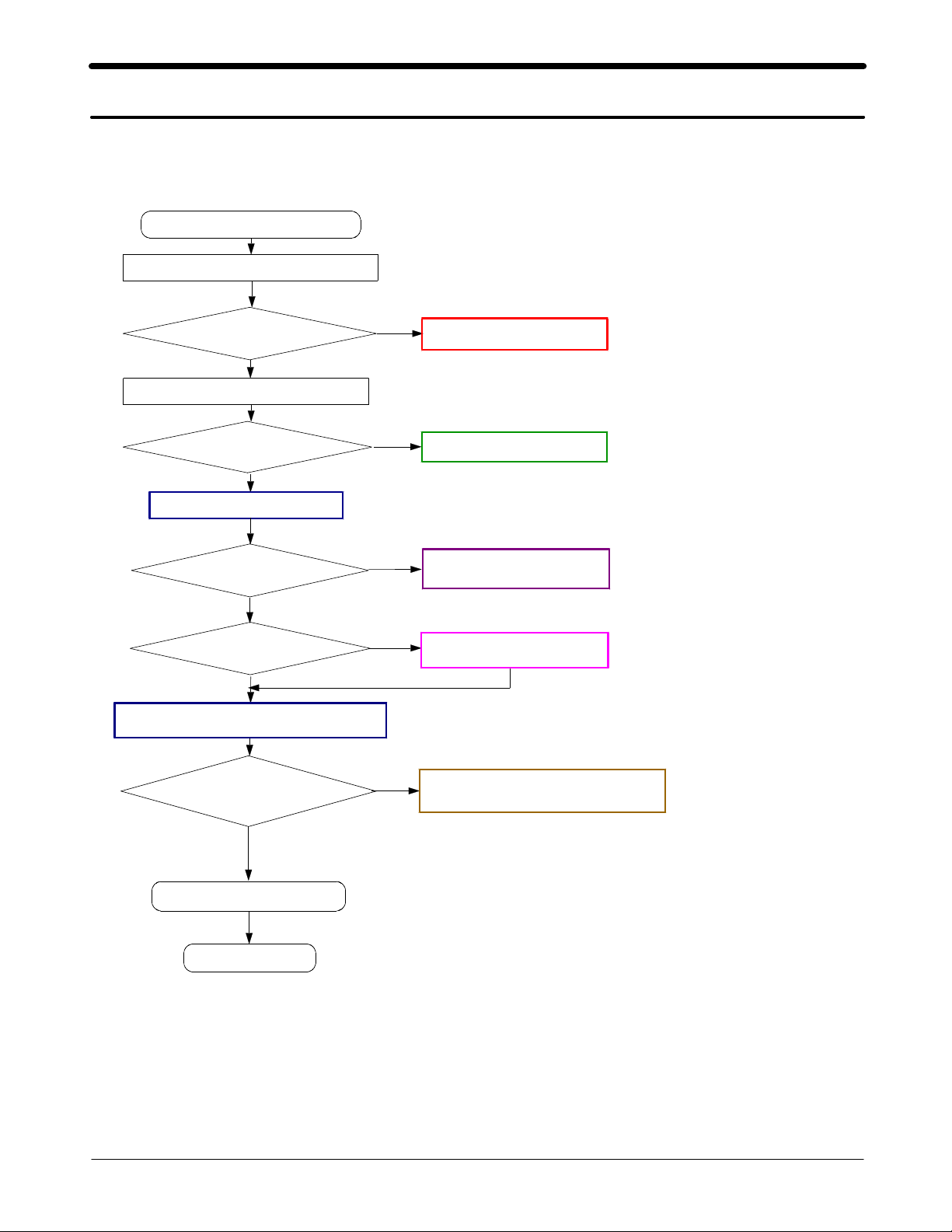
9-1.Baseband
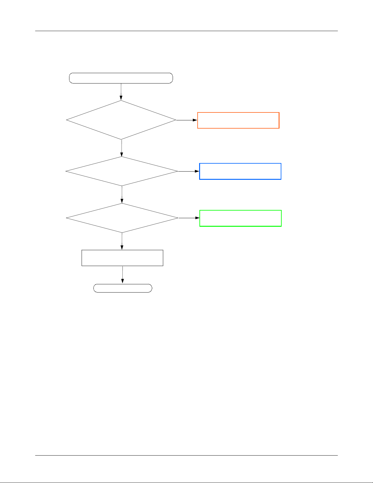
9-1-1. Power ON
'Power On' does not work
Check the current consumption
Yes
Current consumption
>= 100mA
Yes
Check the Vbat Voltage
Voltage >=3.3V
Yes
Check the pin of UCP300
Pin#A6 : 1.8V
Pin#D6 : 2.9V
Yes
Pin#M7 : 2.9V
Pin#L8,#P4 : 1.8V
Yes
Check the clock signal at Pin#12(C120) of RFT100
Yes
No
No
No
No
Download again
Charge the Battery
Check UCP300
C343 and C344
Check UCP300
C300,C301,C303
Freq = 26MHz
Vrms >=300mV
Vpp≒900mV
Yes
Check the initial operation
END
SAMSUNG Proprietary-Contents may change without notice
This Document can not be used without Samsung's authorization
No
Check the clock generation circuit
(related to OSC100, Pin#9, Pin#10)
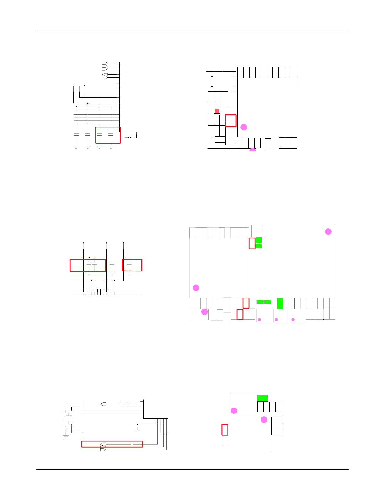
9-1
1
Page 2
Flow Chart of Troubleshooting
RTX_I_P
RTX_Q_N
V
V
V
RTX_Q_P
9
8
8
.
.
.
2
2
1
_
_
_
VAPC
A
D
D
TXPSTB
C
C
C
C
C
C
V
V
V
C337
C342
C343
C344
J3
K3
K4
H5
L5
P13
P12
C10
A6
D6
E14
F12
D14
C15
B15
C12
D13
RXTXIP
RXTXQN
RXTXQP
TXP
TXPSTB
USB_CARKIT_D_N
USB_CARKIT_D_P
USB_CHRG
VLDO_1
VLDO_2
VLDO_AUD
VLDO_AUX1
VLDO_AUX2
VLDO_COREA
VLDO_COREA_S
VLDO_COREB
VLDO_COREC
S
S
V
8
6
K
K
4
C
3
4
1
L300
C
C
C
C
3
3
3
3
3
3
9
7
3
3
3
4
Z
D
6
0
0
C331
C
C
R
3
3
3
C343
0
3
0
6
5
1
D
B
D
D
S
S
N
N
S
S
G
V
V
G
1
9
1
1
K
K
N
C344
C
R
3
3
0
0
R300
5
2
TH300
C605
C
3
2
0
C307
C
C
3
4
2
C
3
3
2
C
R
C
4
4
4
3
2
1
1
3
5
7
5
6
0
0
3
P
C
U
C
C
C
3
3
3
2
2
0
1
8
9
C
R
C
C
3
4
3
3
0
0
2
2
2
8
7
5
T
D
L
F
1
6
1
E
2
2
1
X
A
G
C
C
C
C
3
3
3
3
0
2
2
3
3
4
0
8
C
R
R
C
C
C
4
3
3
3
1
4
4
3
5
1
2
VCCA_2.8V
VCCD_2.9V
C300
4
5
2
7
1
2
1
1
1
N
K
M
C
D
N
C
A
D
D
D
1
B
D
D
D
1
D
V
V
V
D
D
V
D
V
3
0
0
1
C
S
O
4
CLK26M_BT
2
1
CLK26M_DBB
SBCK
SBDT
VCCD_1.8V
C301 C302 C303
0
5
1
5
4
8
1
1
1
L
P
K
L
P
N
L
V
D
R
B
O
O
I
I
T
D
D
K
D
_
_
C
D
P
D
D
D
D
O
V
S
V
V
D
D
A
D
V
V
_
D
D
V
D
V
C117
C120
]
m
’
p
p
0
z
H
,
2
3
0
0
6
RFT100
FSYS3
7
FSYS2
8
VDD2
9
XO
10
1
3
S
XOX
D
D
K
Y
N
L
A
D
S
V
F
C
G
D
3
2
4
1
1
1
1
1
6
0
0
3
P
C
U
C
C
C
C
3
3
3
3
2
2
2
3
0
1
8
2
K
8
6
.
7
2
[
3
6
4
-
C
1
’
M
C
3
C
S
O
2
6
C
C
4
4
3
4
0
2
2
1
5
8
5
7
C
C
C
3
3
3
2
0
3
0
9
8
C
C
3
3
2
R
1
2
6
5
0
0
OSC100
CX3225SB-H2827
C
1
2
0
C
1
2
1
C204
C
C
3
3
0
2
2
7
C206
C
O
C
R
3
E
0
0
T
D
L
F
1
6
1
E
2
2
1
X
A
G
R226
R
C
C
2
3
3
2
4
C
3
0
1
R227
0
0
1
3
V
R
R
2
2
1
0
4
1
C117
C
1
0
7
M
6
2
B
7
1
D
X
1
2
2
A
-
C
5
A
H
2
4
0
F
R
R
C
C
2
2
6
2
R225
0
0
2
1
1
0
2
0
C602 C603 C604
R
C
R
1
1
1
0
0
0
3
8
4
R102
P
U
C
D
2
0
0
V
C
C
C
R
R
R
2
2
2
2
2
0
0
8
9
V
R
6
0
1
6
0
1
0
0
7
2
9
3
V
R
R
C
R
2
2
6
6
0
1
0
0
2
0
0
6
C106
R107
T
1
0
0
R
F
9-2
SAMSUNG Proprietary-Contents may change without notice
This Document can not be used without Samsung's authorization
2
Page 3
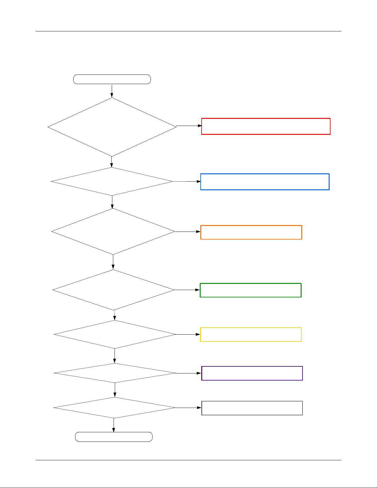
9-1-2. Initial
Flow Chart of Troubleshooting
Initial Failure
Yes
The Pin#A6 of UCP300 =
1.8V and
the Pin#D6 of UCP300 =
2.9V ?
Yes
Is the RST Pin#P5 of
UCP300 "Low→High" ?
Yes
There is 32.768kHz wave
forms at the C326 and C328
of OSC300
Is the SIM_RST Pin #B5 of
UCP300 is "High"
-
Yes
?
No
No
No
No
(if it has some problem, it is to be replaced.)
(if it has some problem, it is to be replaced.)
Check the
Check the
Check the
Check the
UCP300
UCP300
UCP300
UCP300
Yes
The voltage is "High" at the
C300,C301,C302,C303
Yes
LCD display is O.K
Yes
Sound is O.K
Yes
END
SAMSUNG Proprietary-Contents may change without notice
This Document can not be used without Samsung's authorization
No
No
No
9-3
Check the
Check the
Check the
UCP300
LCD
AUDIO
part
part
3
Page 4
Flow Chart of Troubleshooting
CNTL_DAT_CSP
SIM_CLK
SIM_IO
SIM_RST
UP_CLK
UP_IO
UP_RST
VRFLDO_1
VRFLDO_2
VREF
CNTL_EN_CSP
HV_CHRG
BATKELV
CREF
FBSW
PSW1_BUF
RTC_CLK
SCUSTB
VACC
VEXT
VRTC
SCAN
SCANTST
RING_DRV
VIB_DRV
VIB_RNG_EN
SYSCLK
SYSCLKEN
RESETN
RESET_O
X1RTC
X2RTC
VAMICREF
VAMICRTN
VAREF
VAREFRTN
VAVCM
VAVCMLSH
VAVCMRTN
CSN_PSC
SCLK_PSC
SDI_PSC
SDO_PSC
B6
E6
B5
N5
L6
M6
E3
F3
F2
P1
N9
D10
G5
AFC
N7
AINT
B11
F1
L9
DINT
B12
B13
LX
D3
NC1
L10
R3
P3
C9
A12
F5
C5
VSIM
N4
K7
E8
E9
L7
N6
R6
R4
P5
G4
G3
K13
K10
K12
J11
L14
F13
K11
M10
P10
R10
M9
L300
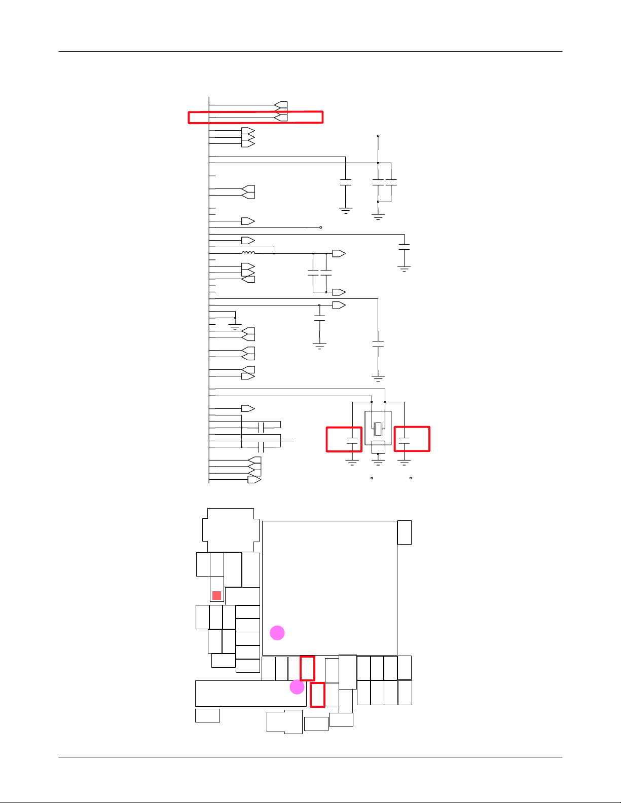
SIM1_CLK
SIM1_DATA
SIM1_RST
CNTL_DAT_CSP
CNTL_EN_CSP
AINT
DINT
PSW1_BUF
RTC_CLK
SCUSTB
MOTOR_EN
VIB_RNG_EN
CLK26M_ABB
CLK_REQ_ABB
FLASH_RST
RST
VAMICREF
C325
C327
UP_CS
UP_SCLK
UP_SDI
UP_SDO
SIM_CLK
SIM_IO
SIM_RST
C310
C307
VBAT
C320
C311
C328
VRF_2.9V
C308
DCDC_OUT
GND_SW
VSIM
23
VBAT
C321
41
C309
C315
OSC300
C326
VBAT
C
3
0
L300
C
C
3
3
3
3
7
9
Z
D
6
0
0
C
R
3
3
0
0
1
6
R
3
0
2
C307
R304
T
D
C
C
3
3
3
3
3
4
C331
C
3
C343
3
5
C344
C
3
R300
0
5
TH300
C
3
2
C605
0
]
’
z
H
,
6
K
2
p
m
7
8
0
p
[
3
6
.
2
0
0
3
C
S
O
0
0
3
P
C
U
C
C
C
3
2
8
C
3
2
6
C329
C
3
0
9
C
3
1
5
C500
3
3
3
2
2
1
-
’
C
M
1
4
0
0
3
Q
L
-
F
1
6
1
E
2
2
1
X
A
G
C
C
3
3
2
3
0
8
C
3
2
R
2
6
0
0
0
R
C
C
2
3
3
0
0
2
1
3
4
V
C
R
R
3
2
2
0
1
0
4
1
1
9-4
SAMSUNG Proprietary-Contents may change without notice
This Document can not be used without Samsung's authorization
4
Page 5
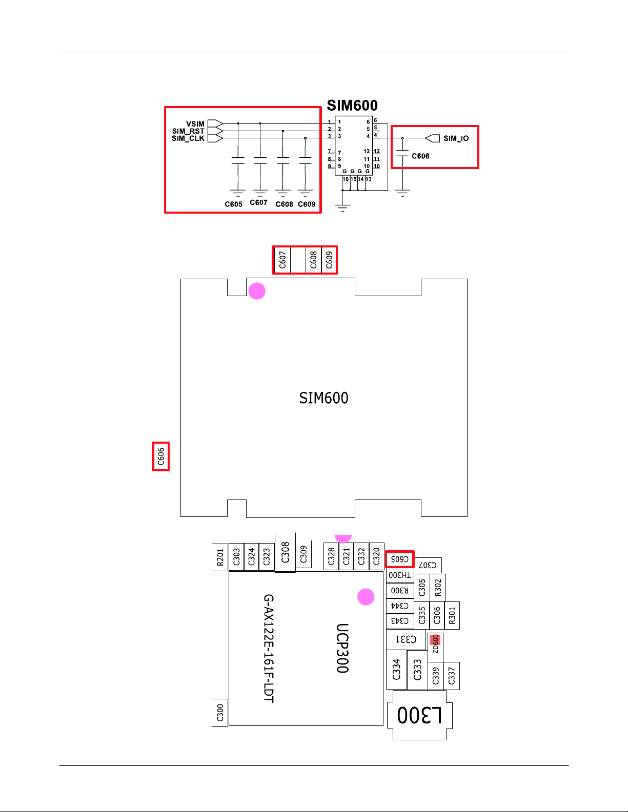
9-1-3. Sim Part
"Insert SIM is displayed on the LCD
Flow Chart of Troubleshooting
Yes
Check the SIM connector's
(SIM600) connection to
SIM card
Yes
Check the voltage at Pin#1
of SIM600 >= 2.9V ?
Yes
Is there any signals
Pin#13,#15,#16 of SIM600 ?
Yes
Check the SIM Card
END
No
No
No
Resolder or change
Check the
Check the
UCP300
UCP300
SIM600
9-5
SAMSUNG Proprietary-Contents may change without notice
This Document can not be used without Samsung's authorization
5
Page 6
Flow Chart of Troubleshooting
9-6
SAMSUNG Proprietary-Contents may change without notice
This Document can not be used without Samsung's authorization
6
Page 7

9-1-4. Microphone Part
Microphone does not work
Flow Chart of Troubleshooting
Yes
Is the assembled status of
microphone O.K?
No
Yes
Check the reference voltage on mic path
Yes
R407≒2.4V ?
No
Yes
No
Is microphone ok?
Yes
END
C413
C419
C414
C418
C415
R410
R408
C417
MONO1_IN_N MIC-
Reassembled the microphone
Resolder or change
R406,R407,C416
Check
UCP300
R406
MIC+MONO1_IN_P
R407
C416
VAMICREF
MIC+
MIC-
L403
L404
C433C432
M
I
C
4
0
0
R
V
4
V
0
0
R
1
4
0
4
0
4
L
0
3
L
4
3
3
4
4
3
2
C
C
1
0
5
A
T
VR400
2
2
6
R
0
0
3
C
0
C
6
2
0
C
4
2
3
1
2
R
3
0
2
C
MIC400
VR401
G
-
A
X
1
2
2
E
-
1
6
1
F
-
L
D
T
5
7
2
2
2
0
3
3
3
C
C
C
8
3
4
1
1
1
4
4
4
C
C
C
7
0
0
R
6
4
4
6
1
4
C
U
C
P
3
0
0
1
6
2
5
7
8
5
1
0
2
4
4
4
C
R
C
9
0
1
1
3
1
4
4
4
C
R
C
R
5
9
1
2
4
4
C
C
6
3
0
1
4
4
C
R
4
3
4
1
3
3
3
4
C
C
C
R
8
1
3
3
2
2
3
4
4
C
C
C
6
1
R
4
4
2
4
C
7
0
4
C
9-7
SAMSUNG Proprietary-Contents may change without notice
This Document can not be used without Samsung's authorization
7
Page 8

Flow Chart of Troubleshooting
9-1-5. Receiver Part
There is no sound from the Receiver
Yes
Is the terminal of Receiver
Is there any signals at the
Pin#R13 and Pin#R14 of
HI_MONO_OUT_N
HI_MONO_OUT_P
O.K ?
UCP300 ?
END
Yes
Yes
R400
R402
C402
No
No
C403
Replace the Receiver
Check
UCP300
Resolder
(OR
R400, R402)
CON400
1
1
2
2
D401D400
HI_MONO_OUT_N
HI_MONO_OUT_P
LO_MONO_OUT_N
LO_MONO_OUT_P
MONO1_IN_N
MONO1_IN_P
MONO2_IN_N
MONO2_IN_P
4
3
1
1
4
4
C
C
4
0
6
R
7
4
1
6
0
0
4
L
1
0
4
L
2
0
4
R
7
P
E
W
0
0
3
0
0
4
4
R
C
UME200
S71WS256PC0HF3SR0
3
1
2
R
3
0
2
C
5
0
4
C
4
0
4
C
2
0
4
C
9-8
SAMSUNG Proprietary-Contents may change without notice
This Document can not be used without Samsung's authorization
8
R13
HI_MONO_OUT_N
R14
HI_MONO_OUT_P
R12
LO_MONO_OUT_N
P11
LO_MONO_OUT_P
G13
MONO1_IN_N
J13
MONO1_IN_P
G12
MONO2_IN_N
G11
MONO2_IN_P
9
8
0
1
1
1
4
4
4
C
C
R
R
4
0
5
9
1
2
4
4
C
C
9
8
7
4
0
0
1
4
C
C
3
6
1
0
4
4
R
C
8
X
M
A
1
3
C
U
4
0
0
1
2
1
1
4
4
C
C
1
3
1
2
2
3
4
4
4
C
C
C
4
1
R
6
4
2
4
C
7
0
4
C
9
1
3
C
C
1
0
4
C
Page 9

9-1-6. Speaker Part
There is no sound from the Buzzer
Flow Chart of Troubleshooting
Yes
Is the terminal of Speaker
O.K ?
Yes
Is there any signals at the
Pin#R13 and Pin#R14 of
UCP300 ?
Yes
END
LO_MONO_OUT_N
LO_MONO_OUT_P
STEREO_OUT_R
STEREO_OUT_L
SDA
SCL
C406
C400
C407
VBAT
C411
C401
No
Replace the Speaker
No
1
5
B
C
D
D
D
D
V
V
P
3
D
U400
D
N
G
3
A
OUT+
D
N
S
S
G
V
P
4
C
C412
OUT-
HPR
HPL
C1N
C1P
D5
B5
A1
A2
A4
A5
1
NC
2
NC
D4
RXIN-
B4
RXIN+
D2
INA1
D1
INA2
C2
INB1
C1
INB2
B2
BIAS
B3
SDA
C3
SCL
(OR
R404
R405
Check
Resolder
L400
L401
C410
UCP300
L400, L401)
C408
C409
SPK_N
SPK_P
EAR_R
EAR_L
UME200
S71WS256PC0HF3SR0
8
4
1
3
4
1
C
2
R
4
0
7
3
0
2
C
5
0
0
0
4
4
L
C
4
1
0
0
4
4
L
C
2
0
2
0
0
0
4
4
4
C
R
R
0
3
1
1
1
4
4
4
C
R
C
R
R
0
6
4
5
1
4
C
1
6
4
C
3
1
4
R
7
P
9
W
7
8
X
E
A
M
U
4
0
0
3
0
2
0
1
1
4
4
4
C
C
C
3
1
9
2
3
1
4
4
4
C
C
C
9
4
2
2
4
4
C
C
6
7
0
0
4
4
C
C
8
9
1
1
3
3
C
C
4
C
0
0
1
1
0
1
4
4
C
C
9-9
SAMSUNG Proprietary-Contents may change without notice
This Document can not be used without Samsung's authorization
9
Page 10

Flow Chart of Troubleshooting
9-1-7. Charging Part
Abnormal charging part
What is the type of Charging?
Yes
TA Charging
Is the U300
VEXT(Pin#1)≒5V ?
Yes
Is the U300
CHG_ON(Pin#6) "LOW"?
ABI,ABO "HIGH"?
Yes
Charging Current is
100mA ~ 450mA ?
Yes
Check The Battery
No
No
No
Check
Check
Check
IFC500
UCD200
U300
END
9-10
SAMSUNG Proprietary-Contents may change without notice
This Document can not be used without Samsung's authorization
10
Page 11

Flow Chart of Troubleshooting
EAR_MIC+
EAR_MIC-
EAR_R
EAR_L
EAR_SW
EAR_JACK_IN
SDS_TXD
SDS_RXD
JIG_ON_IF
USB_D+
USB_D-
C503
VEXT_5V
VCCD_1.8V
RADIO_ANT
VBAT
L500
R500
IFC500
1
1
2
L501
L503
ZD500
0
0
5
R
V
1
2
3
6
5
4
ZD501
1
2
3
6
5
4
C504
VBAT
VEXT_5V
VCCD_1.8V
R505
L504
L502
R501
R502
R503
R504
R508
5
0
5
L
2
3
3
4
4
5
5
6
6
7
7
8
8
9
9
10
10
11
11
12
12
13
13
14
14
15
15
16
16
17
17
18
18
19
19
20
20
21
NC
22
NC
23
NC
24
NC
25
NC
26
NC
27
NC
SDS_TXD_J
SDS_RXD_J
JIG_ON_IF_J
U300
1
IN
2
GND
36
C313
1
0
5
C
MIC5235-5.0YM5
9
4
3
3
0
U301
2
3
C
ISET
ABI ABO
C
Q
3
0
0
ICHRG CHG_ON
JIG_ON_IF
R304
C312
2
7
6
0
0
0
5
5
5
C
R
R
U500
RT9363APQW
0
5
C
0
8
BATT
7
_POK|
_EN|
5
D
N
G
9
R305
5
0
3
R
T
E
A
4
1
0
0
0
3
3
R
6
0
3
R
4
1
3
C
C314
3
8
8
3
4
R303
1
3
C
X
A
M
U
2
1
3
C
0
3
R
CHG_DET
JIG_ON
9-11
SAMSUNG Proprietary-Contents may change without notice
This Document can not be used without Samsung's authorization
11
Page 12

Flow Chart of Troubleshooting
9-1-8. FM Receiver part
Abnormal FM part
What is the type of Charging?
Yes
TA Charging
Check the voltage at Pin#10,
Pin#11 of U401.
Is it OK?
Yes
Is there any signals at the
Pin#R13 and Pin#R14 of
U401 ?
Yes
Is there any signals at the
Pin#M13 and Pin#M14 of
UCP300 ?
Yes
END
No
No
No
Resolder or change
Resolder or change
Check
UCP300
(or Resolder
C318, C319
U401
U401
)
9-12
SAMSUNG Proprietary-Contents may change without notice
This Document can not be used without Samsung's authorization
12
Page 13

RADIO_ANT
C420
FM_BUS_EN
L402
Flow Chart of Troubleshooting
VCCD_1.8V
VCCD_2.9V
R420R419
R409
R411
2223
21
19
18 17
20
C
C
D
1
T
C
N
N
N
N
G
1
NC
2
FMI
RFGND
LPI
RST
SEN
U401
K
O
L
I
C
D
S
S
7
8
3
4
5
611
K
L
O
N
I
P
C
_
|
D
G
2
|
3
O
DFS
O
P
P
G
G
DOUT
LOUT
ROUT
GND
K
VDD
L
O
C
I
V
R
10
9
R412
16
15
R414
14
13
12
FM_INT
PCM_CLK
PCM_SYNC
PCM_RXD
RADIO_L
RADIO_R
FM_SCL
FM_SDA
RTC_CLK
C428C426
C427
R421
C434
RADIO_L
RADIO_R
STEREO_OUT_L
STEREO_OUT_R
G
-
A
X
1
2
2
E
-
1
6
1
F
-
L
D
R
6
2
2
C
2
0
6
C
2
0
4
T
0
0
3
C
3
1
2
R
3
0
2
C
5
0
4
C
4
0
4
C
2
0
4
C
5
7
2
2
2
0
3
3
3
C
C
C
3
4
8
1
1
1
4
4
4
C
C
C
R
4
6
0
R
4
0
7
4
1
C
6
0
9
P
8
W
X
7
A
7
E
0
4
L
4
0
U
0
1
0
4
L
0
3
0
2
1
0
0
0
4
4
4
4
C
C
R
R
C316
C317
C318
JIG_ON
PWR_ON
U
C
P
3
0
0
5
1
4
R
3
2
4
C
1
6
9
1
3
C
9
0
4
C
C319
2
6
4
3
3
3
C
C
1
8
2
3
4
3
C
C
R
4
0
2
PWR_KEEP
5
7
8
2
1
0
4
4
4
C
C
R
1
9
0
1
3
1
4
4
4
R
C
C
5
4
9
1
2
2
4
4
4
C
C
C
7
6
3
0
0
1
4
4
4
C
C
R
8
M
1
3
C
C
4
0
0
1
1
2
0
1
1
4
4
4
C
C
C
8
0
4
C
K15
STEREO1_IN_L
K14
STEREO1_IN_R
H11
STEREO2_IN_L/M
J12
STEREO2_IN_R/M
M14
STEREO_OUT_L
M13
STEREO_OUT_R
P6
PWR_KEEP
E5
PWR_SW2
C4
PWR_SW1N
T
H
3
0
0
5
2
R
3
0
0
0
0
3
3
C
R
3
4
4
C
6
5
1
0
3
C
3
4
3
3
1
4
3
3
C
1
4
3
C
0
4
3
C
6
7
1
1
3
3
C
C
1
0
4
U
L
4
0
3
3
3
C
C
R
3
C
0
0
6
D
Z
3
3
7
9
3
3
3
3
3
C
C
C
L
3
0
0
4
0
0
1
3
1
1
C
3
3
C
C
5
0
G
R
4
2
0
C
4
2
8
4
1
3
2
4
4
C
R
R
7
M
G
0
2
6
B
5
0
9
7
4
I
S
9
5
C
4
2
C
4
2
R
4
0
R
4
1
9-13
SAMSUNG Proprietary-Contents may change without notice
This Document can not be used without Samsung's authorization
13
Page 14

Flow Chart of Troubleshooting
9-2. RF
10-2-1. EGSM RX
Continuous Rx on, Rx input=-60dBm, Channel=37
NORMAL CONDITION
catch the channel?
YES
PAM100 CHECK
Pin#17≥-65dBm ?
YES
PAM100 CHECK
Pin#12≥-65dBm ?
YES
F100 CHECK
Pin#6, #7≥-65dBm ?
YES
RFT100 CHECK
Pin#22, #23≥-65dBm ?
YES
RFT100 CHECK
Pin#12 : 26MHz
NO
NO
NO
ANT, ANT_PAD, L102, C125
NO
RFS100,L100,L101,C104
resolder or change
NO
resolder or change
NO
resolder or change
resolder or change
resolder or change
CHECK
contact ?
PAM100
F100
RFT100
OSC100
YES
RFT100 CHECK
Pin#1,#2,#3,#4
Vp-p : 550mV?
YES
GSM Receiver is OK?
END
NO
NO
RFT100
resolder or change
GSM RX path componet
resolder or change
9-14
SAMSUNG Proprietary-Contents may change without notice
This Document can not be used without Samsung's authorization
14
Page 15

9-2-2. DCS RX
Flow Chart of Troubleshooting
Continuous Rx on, Rx input=-60dBm, Channel=698
NORMAL CONDITION
catch the channel?
YES
PAM100 CHECK
Pin#17≥-65dBm ?
YES
PAM100 CHECK
Pin#13≥-65dBm ?
YES
F100 CHECK
Pin#8, #9≥-65dBm ?
YES
RFT100 CHECK
Pin#19, #20≥-65dBm ?
YES
RFT100 CHECK
Pin#12 : 26MHz
NO
NO
NO
ANT, ANT_PAD, L102, C125
NO
RFS100,L100,L101,C104
resolder or change
NO
resolder or change
NO
resolder or change
resolder or change
resolder or change
CHECK
contact ?
PAM100
F100
RFT100
OSC100
YES
RFT100 CHECK
Pin#1, #2, #3, #4
Vp-p : 550mV?
YES
DCS Receiver is OK?
END
NO
NO
RFT100
resolder or change
DCS RX path componet
resolder or change
9-15
SAMSUNG Proprietary-Contents may change without notice
This Document can not be used without Samsung's authorization
15
Page 16

Flow Chart of Troubleshooting
9-2-3. EGSM TX
MS TX level 19, CH : 62, RBW : 100KHz, VBW : 100KHz, SPAN : 10MHz, REF LEV. : 10dBm
Check PAM100
Pin#17=2~5dBm
Yes
Check and Change
RFS100, L104, C100
L101, L100, C104
No
PAM100 TX_EN
Pin #4 : 2.85V ?
Yes
PAM100 VBATT
Pin #30 :3.8V
Yes
PAM100 BS1
Pin #5="LOW"
Yes
PAM100 VLOGIC
Pin #2="HIGH"
Yes
PAM100 VRAMP
Pin #3≤1.8V ?
Yes
Check PAM100
Pin #27=-5dBm
No
Check and Change
No
Check the battery
No
Check and Change
No
No
Check and Change
No
UCP300
block
UCP300
UCP300
Check or Change
RFT100
Check or Change
UCP300
NO
Yes
Check and Change
PAM100
Check RFT100
Pin#28=1.5~5.5dBm
RFT100
YES
RFT100
RFT100
Pin#1,#2,#3,#4
=550mV
No
YES
Pin#12=26MHz
Check or Change
9-16
SAMSUNG Proprietary-Contents may change without notice
This Document can not be used without Samsung's authorization
16
Yes
NO
Check or Change
OSC100
Page 17

9-2-5. DCS/PCS TX
DCS: MS TX level 15 CH : 698, RBW : 100KHz, VBW : 100KHz, SPAN : 10MHz, REF LEV. : 10dBm
Flow Chart of Troubleshooting
Check PAM100
Pin#17=2~5dBm
Yes
Check and Change
RFS100, L104, C100
L101, L100, C104
No
PAM100 TX_EN
Pin #4 : 2.85V ?
Yes
PAM100 VBATT
Pin #30 :3.8V
Yes
PAM100 BS1
Pin #5="HIGH"
Yes
PAM100 VLOGIC
Pin #2="HIGH"
Yes
PAM100 VRAMP
Pin #3≤1.8V ?
Yes
Check PAM100
Pin #29=-5dBm
Yes
No
Check and Change
No
Check the battery
Check and Change
No
No
No
Check and Change
No
UCP300
block
UCP300
UCP300
Check or Change
RTF100
Check or Change
UCP300
NO
Check and Change
PAM100
Check RFT100
Pin#28=1.5~5.5dBm
RFT100
NO
RFT100
RFT100
Pin#1,#2,#3,#4
=550mV
No
YES
Pin#12=26MHz
Check or Change
9-17
SAMSUNG Proprietary-Contents may change without notice
This Document can not be used without Samsung's authorization
17
Yes
NO
Check or Change
OSC100
Page 18

Flow Chart of Troubleshooting
VRF_2.9V
R104
1
2
3
4
5
6
7
8
9
10
VRF_2.9V
R102
C106
A
AX
B
BX
VDD1
FSYS3
FSYS2
VDD2
XO
XOX
C
N
VRF_2.9V
R103
C107
RTX_I_P
RTX_I_N
RTX_Q_P
RTX_Q_N
CLK26M_BT
3
2
0
0
1
C
S
O
4
1
CLK26M_DBB
SBCK
SBDT
SBLE
C108
C117
C120
VRF_1.5V
7
0
1
5
3
R
3
4
3
3
C
D
D
N
N
N
G
G
RFT100
1
S
D
Y
N
S
F
G
1
1
8
9
2
0
1
2
2
3
3
3
5
1
6
2
F
X
X
D
E
D
T
T
D
R
D
VDD4
V
V
R
RX1X
RX1
RX2X
RX2
GND
RX3X
RX3
RX4X
3
RX4
D
K
A
L
N
D
D
E
V
C
5
6
2
3
4
1
1
1
1
1
VRF_1.5V
C110C109
C111
C112
7
2
26
25
24
23
22
21
20
19
18
17
DCS_LNA_IN_N
VRF_1.5V
C121
R105
R106
GSM_PAM_IN
DPCS_PAM_IN
UCD200
SAMSUNG Proprietary-Contents may change without notice
This Document can not be used without Samsung's authorization
OCTL_0
OCTL_1
OCTL_2
OCTL_3
OCTL_4
OCTL_5
OCTL_6
OCTL_7
T18
P17
M15
N18
P19
N15
P18
R17
9-18
18
BAND_SEL
VMOD_EN
TX_EN
Page 19

Flow Chart of Troubleshooting
DCS_LNA_IN_N
DCS_LNA_IN_P
GSM_LNA_IN_N
GSM_LNA_IN_P
C119
C122
C123
C124
C105
RFS100
G
G
C
C116
C118
A
4
3
1
2
R100
R101
L102
R108
VMOD_EN
VAPC
TX_EN
GSM_PAM_IN
DPCS_PAM_IN
C101
ANT100
TP
ANT101
TP
ANT102
TP
VBAT
C103C102
5
BS1
6
BS2
12
RX1
13
RX2
11
NC
14
NC
G
4
3
1
1
1
C
F100
L107
9
BAL1
8
OUT1
7
L108
BAL2
6
OUT2
G
510
6
1
3
C
1
IN1
4
IN2
G2G3G
PAM100
G
G
G
G
G
G
G
G
G
5
3
4
2
1
8
6
5
3
3
3
3
3
2
2
2
L100
L101
C104
0
7
3
1
T
T
T
N
A
A
G
G
0
2
G
G
9
8
1
1
VLOGIC
VRAMP
TX_EN
GSM_IN
DCS|PCS_IN
G
G
G
G
6
5
0
1
1
1
9
G
G
7
8
B
V
G
G
G
3
2
1
4
2
2
2
2
C100
L103
2
3
4
27
29
1
L104
C115
C
1
4
0
0
1
M
A
P
1
C
1
C
1
1
2
0
C
F
1
1
1
0
L
1
C
1
3
0
C
1
5
0
C
1
5
1
R
1
8
0
C
1
8
1
C
1
0
C
1
6
1
3
0
1
C
2
R
C
L
1
1
1
0
0
1
5
6
2
9
1
0
7
1
C
2
2
L
1
1
C
2
3
0
8
1
C
2
4
C
C
1
1
0
1
9
0
2
O
S
C
0
0
1
T
F
R
R
R
C
1
1
1
0
0
0
2
7
6
1
0
0
C
0
1
7
C
1
1
7
R
0
1
3
C
0
1
8
R
0
1
4
3
0
1
L
2
0
1
T
N
A
0
0
1
T
N
A
1
0
1
T
N
A
4
0
1
L
C
1
1
0
C
1
2
5
0
2
1
L
C
4
1
0
C
1
0
0
L
1
0
0
L
0
1
1
001SFR
R
1
0
0
R
C
L
1
1
1
0
0
1
6
5
1
9-19
SAMSUNG Proprietary-Contents may change without notice
This Document can not be used without Samsung's authorization
19
 Loading...