

Page 1

AlphaPC 164UX/BX Motherboard
Technical Reference Manual
Preliminary
Page 2

Notice
The information in this publication has been carefully checked and is believed to be entirely accurate at the time of publication.
Samsung assumes no responsibility, however, for possible errors or omissions, or for any consequences resulting from the use
of the information contained herein.
Samsung reserves the right to make changes in its products or product specifications with the intent to improve function or
design at any time and without notice and is not required to update this documentation to reflect such changes.
This publication does not convey to a purchaser of semiconductor devices described herein any license under the patent rights of
Samsung or others.
AlphaPC 164UX/BX Motherboard
Technical Reference Manual
©1998 Samsung Electronics
All rights reserved. No part of this publication may be reproduced, stored in a retrieval system, or transmitted in any form or by
any means, electric or mechanical, by photocopying, recording, or otherwise, without the prior written consent of Samsung
Electronics.
Samsung and Samsung logo are trademarks of Samsung Electronics Co., Ltd.
Alpha, Digital Semiconductor are trademarks of Digital Equipment Corporation.
FaxBACK and Intel are registered trademarks of Intel Corporation.
GRAFOIL is a registered trademark of Union Carbide Corporation.
Microsoft, MS-DOS, Windows, and Windows 95 are registered trademarks and Windows NT is a trademark of Microsoft
Corporation.
Dallas is a registered trademark of Dallas Semiconductor Corporation.
Q is a registered trademark of Quality Semiconductor,Inc.
SYMBIOS is a registered trademark of Symbios,Inc.
AMD is a registered trademark of Advanced Micro Devices,Inc.
SMC is a registered trademark of Standard Microsystems Corporation.
All other trademarks and registered trademarks are the property of their respective owners.
San #24 Nongseo-ri, Kiheung-eup
Yongin-city, Kyungki-do, Korea
449-900
FAX : 82-331-209-4492
TEL : 82-331-209-3282
Printed in the Republic of Korea
Page 3

Contents
Preface
1 Introduction to the AlphaPC 164UX Motherboard
1.1 System Components and Features . . . . . . . . . . . . . . . . . . . . . . . . . . . . . . . . . . . 1–1
1.1.1 Digital Semiconductor 21174 Core Logic Chip . . . . . . . . . . . . . . . . . . . . . . . 1–3
1.1.2 Memory Subsystem . . . . . . . . . . . . . . . . . . . . . . . . . . . . . . . . . . . . . . . . . . . . 1–3
1.1.3 L3 Bcache Subsystem Overview . . . . . . . . . . . . . . . . . . . . . . . . . . . . . . . . . . 1–5
1.1.4 PCI Interface Overview . . . . . . . . . . . . . . . . . . . . . . . . . . . . . . . . . . . . . . . . . 1–6
1.1.5 ISA Interface Overview . . . . . . . . . . . . . . . . . . . . . . . . . . . . . . . . . . . . . . . . . 1–6
1.1.6 Miscellaneous Logic . . . . . . . . . . . . . . . . . . . . . . . . . . . . . . . . . . . . . . . . . . . 1–6
1.2 Software Support . . . . . . . . . . . . . . . . . . . . . . . . . . . . . . . . . . . . . . . . . . . . . . . . . 1–7
1.2.1 ARCSBIOS Windows NT Firmware. . . . . . . . . . . . . . . . . . . . . . . . . . . . . . . . 1–7
1.3 Hardware Design Support. . . . . . . . . . . . . . . . . . . . . . . . . . . . . . . . . . . . . . . . . . . 1–7
2 System Configuration and Connectors
2.1 AlphaPC 164UX Jumper Configuration . . . . . . . . . . . . . . . . . . . . . . . . . . . . . . . . 2–3
2.2 CPU Speed Selection (Option 1,2,3,&4). . . . . . . . . . . . . . . . . . . . . . . . . . . . . . . . 2–5
2.3 Bcache Size Jumpers (Option 14,15) . . . . . . . . . . . . . . . . . . . . . . . . . . . . . . . . . . 2–5
2.4 Boot Option Jumper (Option 11) . . . . . . . . . . . . . . . . . . . . . . . . . . . . . . . . . . . . . . 2–5
2.5 AlphaPC 164UX Connector Pinouts . . . . . . . . . . . . . . . . . . . . . . . . . . . . . . . . . . . 2–5
2.5.1 PCI Bus Connector Pinouts. . . . . . . . . . . . . . . . . . . . . . . . . . . . . . . . . . . . . . 2–5
2.5.2 ISA Expansion Bus Connector Pinouts . . . . . . . . . . . . . . . . . . . . . . . . . . . . . 2–8
2.5.3 SDRAM DIMM Connector Pinouts. . . . . . . . . . . . . . . . . . . . . . . . . . . . . . . . . 2–9
2.5.4 EIDE Drive Bus Connector Pinouts . . . . . . . . . . . . . . . . . . . . . . . . . . . . . . . . 2–10
2.5.5 Diskette Drive Bus Connector Pinouts. . . . . . . . . . . . . . . . . . . . . . . . . . . . . . 2–11
2.5.6 Parallel Bus Connector Pinouts . . . . . . . . . . . . . . . . . . . . . . . . . . . . . . . . . . . 2–11
2.5.7 COM1/COM2 Serial Line Connector Pinouts. . . . . . . . . . . . . . . . . . . . . . . . . 2–12
2.5.8 Keyboard/Mouse Connector Pinouts . . . . . . . . . . . . . . . . . . . . . . . . . . . . . . . 2–12
2.5.9 Input Power Connector Pinouts. . . . . . . . . . . . . . . . . . . . . . . . . . . . . . . . . . . 2–13
iii
Page 4

2.5.10 Narrow SCSI Bus Connector. . . . . . . . . . . . . . . . . . . . . . . . . . . . . . . . . . . . . 2–13
2.5.11 Fast and Wide SCSI Bus Connector . . . . . . . . . . . . . . . . . . . . . . . . . . . . . . . 2–14
2.5.12 10/100 Mbit Ethernet Connector Pinouts. . . . . . . . . . . . . . . . . . . . . . . . . . . . 2–14
2.5.13 Speaker Connector Pinouts. . . . . . . . . . . . . . . . . . . . . . . . . . . . . . . . . . . . . . 2–15
2.5.14 Microprocessor Fan Power Connector Pinouts . . . . . . . . . . . . . . . . . . . . . . . 2–15
2.5.15 Pin Power LED Connector Pinouts . . . . . . . . . . . . . . . . . . . . . . . . . . . . . . . . 2–15
2.5.16 IDE Drive LED Connector Pinouts. . . . . . . . . . . . . . . . . . . . . . . . . . . . . . . . . 2–16
2.5.17 Reset Switch Connector Pinouts . . . . . . . . . . . . . . . . . . . . . . . . . . . . . . . . . . 2–16
2.5.18 Soft Power Connector Pinouts. . . . . . . . . . . . . . . . . . . . . . . . . . . . . . . . . . . . 2–16
2.5.19 SCSI LED Connector Pinouts . . . . . . . . . . . . . . . . . . . . . . . . . . . . . . . . . . . . 2–16
3 Functional Description
3.1 AlphaPC 164UX Bcache Interface . . . . . . . . . . . . . . . . . . . . . . . . . . . . . . . . . . . . 3–2
3.2 Digital Semiconductor 21174 Core Logic Chip . . . . . . . . . . . . . . . . . . . . . . . . . . . 3–2
3.2.1 21174 Chip Overview . . . . . . . . . . . . . . . . . . . . . . . . . . . . . . . . . . . . . . . . . . 3–3
3.2.2 Main Memory Interface . . . . . . . . . . . . . . . . . . . . . . . . . . . . . . . . . . . . . . . . . 3–4
3.2.3 PCI Devices . . . . . . . . . . . . . . . . . . . . . . . . . . . . . . . . . . . . . . . . . . . . . . . . . . 3–4
3.2.4 System-IO (SIO) Chip . . . . . . . . . . . . . . . . . . . . . . . . . . . . . . . . . . . . . . . . . . 3–6
3.2.5 Ethernet LAN Controller Chip . . . . . . . . . . . . . . . . . . . . . . . . . . . . . . . . . . . . 3–6
3.2.6 PCI-Ultra SCSI (Fast-20) I/O Processor Chip . . . . . . . . . . . . . . . . . . . . . . . . 3–7
3.2.7 PCI Expansion Slots . . . . . . . . . . . . . . . . . . . . . . . . . . . . . . . . . . . . . . . . . . . 3–8
3.3 ISA Bus Devices . . . . . . . . . . . . . . . . . . . . . . . . . . . . . . . . . . . . . . . . . . . . . . . . . . 3–8
3.3.1 Combination Controller . . . . . . . . . . . . . . . . . . . . . . . . . . . . . . . . . . . . . . . . . 3–9
3.3.2 XD Bus Device. . . . . . . . . . . . . . . . . . . . . . . . . . . . . . . . . . . . . . . . . . . . . . . . 3–10
3.3.3 ISA Expansion Slots . . . . . . . . . . . . . . . . . . . . . . . . . . . . . . . . . . . . . . . . . . . 3–10
3.3.4 ISA I/O Address Map. . . . . . . . . . . . . . . . . . . . . . . . . . . . . . . . . . . . . . . . . . . 3–10
3.4 Flash ROM Address Map . . . . . . . . . . . . . . . . . . . . . . . . . . . . . . . . . . . . . . . . . . . 3–10
3.5 Interrupts. . . . . . . . . . . . . . . . . . . . . . . . . . . . . . . . . . . . . . . . . . . . . . . . . . . . . . . . 3–11
3.6 System Clocks . . . . . . . . . . . . . . . . . . . . . . . . . . . . . . . . . . . . . . . . . . . . . . . . . . . 3–15
3.7 Reset and Initialization . . . . . . . . . . . . . . . . . . . . . . . . . . . . . . . . . . . . . . . . . . . . . 3–17
3.8 DC Power Distribution. . . . . . . . . . . . . . . . . . . . . . . . . . . . . . . . . . . . . . . . . . . . . . 3–18
4 Upgrading the AlphaPC 164UX
4.1 Upgrading SDRAM Memory . . . . . . . . . . . . . . . . . . . . . . . . . . . . . . . . . . . . . . . . . 4–1
4.2 Increasing Microprocessor Speed. . . . . . . . . . . . . . . . . . . . . . . . . . . . . . . . . . . . . 4–1
4.2.1 Preparatory Information. . . . . . . . . . . . . . . . . . . . . . . . . . . . . . . . . . . . . . . . . 4–2
4.2.2 Required Tools . . . . . . . . . . . . . . . . . . . . . . . . . . . . . . . . . . . . . . . . . . . . . . . 4–2
4.2.3 Removing the 21164 Microprocessor . . . . . . . . . . . . . . . . . . . . . . . . . . . . . . 4–2
4.2.4 Installing the 21164 Microprocessor . . . . . . . . . . . . . . . . . . . . . . . . . . . . . . . 4–3
iv
Page 5

5 Power and Environmental Requirements
5.1 Power Requirements . . . . . . . . . . . . . . . . . . . . . . . . . . . . . . . . . . . . . . . . . . . . . . 5–1
5.2 Environmental Requirements . . . . . . . . . . . . . . . . . . . . . . . . . . . . . . . . . . . . . . . . 5–1
5.3 Physical Parameters. . . . . . . . . . . . . . . . . . . . . . . . . . . . . . . . . . . . . . . . . . . . . . . 5–2
5.3.1 Board Dimensions . . . . . . . . . . . . . . . . . . . . . . . . . . . . . . . . . . . . . . . . . . . . . 5–2
5.3.2 Board Measurements and Hole Locations. . . . . . . . . . . . . . . . . . . . . . . . . . . 5–3
5.3.3 Board Vertical Clearance. . . . . . . . . . . . . . . . . . . . . . . . . . . . . . . . . . . . . . . . 5–4
5.3.4 ATX I/O Shield Requirements . . . . . . . . . . . . . . . . . . . . . . . . . . . . . . . . . . . . 5–5
A System Address Space
A.1 Address Map. . . . . . . . . . . . . . . . . . . . . . . . . . . . . . . . . . . . . . . . . . . . . . . . . . . . . A–1
A.2 PCI Address Space. . . . . . . . . . . . . . . . . . . . . . . . . . . . . . . . . . . . . . . . . . . . . . . . A–6
A.3 21164 Address Space. . . . . . . . . . . . . . . . . . . . . . . . . . . . . . . . . . . . . . . . . . . . . . A–7
A.3.1 System Address Map. . . . . . . . . . . . . . . . . . . . . . . . . . . . . . . . . . . . . . . . . . . A–10
A.4 21164 Byte/Word PCI Space . . . . . . . . . . . . . . . . . . . . . . . . . . . . . . . . . . . . . . . . A–12
A.4.1 21164 Size Field . . . . . . . . . . . . . . . . . . . . . . . . . . . . . . . . . . . . . . . . . . . . . . A–14
A.5 Cacheable Memory Space . . . . . . . . . . . . . . . . . . . . . . . . . . . . . . . . . . . . . . . . . . A–15
A.6 PCI Dense Memory Space . . . . . . . . . . . . . . . . . . . . . . . . . . . . . . . . . . . . . . . . . . A–15
A.7 PCI Sparse Memory Space . . . . . . . . . . . . . . . . . . . . . . . . . . . . . . . . . . . . . . . . . A–17
A.7.1 Hardware Extension Register (HAE_MEM). . . . . . . . . . . . . . . . . . . . . . . . . . A–18
A.7.2 Memory Access Rules and Operation . . . . . . . . . . . . . . . . . . . . . . . . . . . . . . A–18
A.8 PCI Sparse I/O Space. . . . . . . . . . . . . . . . . . . . . . . . . . . . . . . . . . . . . . . . . . . . . . A–23
A.8.1 Hardware Extension Register (HAE_IO) . . . . . . . . . . . . . . . . . . . . . . . . . . . . A–23
A.8.2 PCI Sparse I/O Space Access Operation . . . . . . . . . . . . . . . . . . . . . . . . . . . A–23
A.9 PCI Configuration Space . . . . . . . . . . . . . . . . . . . . . . . . . . . . . . . . . . . . . . . . . . . A–26
A.10 PCI Special/Interrupt Cycles . . . . . . . . . . . . . . . . . . . . . . . . . . . . . . . . . . . . . . . . . A–31
A.11 Hardware-Specific and Miscellaneous Register Space . . . . . . . . . . . . . . . . . . . . A–31
A.12 PCI to Physical Memory Address . . . . . . . . . . . . . . . . . . . . . . . . . . . . . . . . . . . . . A–32
A.13 Direct-Mapped Addressing . . . . . . . . . . . . . . . . . . . . . . . . . . . . . . . . . . . . . . . . . . A–37
A.14 Scatter-Gather Addressing . . . . . . . . . . . . . . . . . . . . . . . . . . . . . . . . . . . . . . . . . . A–38
A.15 Scatter-Gather TLB. . . . . . . . . . . . . . . . . . . . . . . . . . . . . . . . . . . . . . . . . . . . . . . . A–40
A.15.1 Scatter-Gather TLB Hit Process . . . . . . . . . . . . . . . . . . . . . . . . . . . . . . . . . . A–42
A.15.2 Scatter-Gather TLB Miss Process . . . . . . . . . . . . . . . . . . . . . . . . . . . . . . . . . A–42
A.16 Suggested Use of a PCI Window . . . . . . . . . . . . . . . . . . . . . . . . . . . . . . . . . . . . . A–44
A.16.1 Peripheral Component Architecture Compatibility Addressing and Holes. . . A–45
A.16.2 Memory Chip Select Signal mem_cs_l . . . . . . . . . . . . . . . . . . . . . . . . . . . . . A–45
B Supporting Products
B.1 Memory. . . . . . . . . . . . . . . . . . . . . . . . . . . . . . . . . . . . . . . . . . . . . . . . . . . . . . . . . B–1
B.2 Thermal Products . . . . . . . . . . . . . . . . . . . . . . . . . . . . . . . . . . . . . . . . . . . . . . . . . B–3
B.3 Power Supply . . . . . . . . . . . . . . . . . . . . . . . . . . . . . . . . . . . . . . . . . . . . . . . . . . . . B–3
v
Page 6

B.4 Enclosure . . . . . . . . . . . . . . . . . . . . . . . . . . . . . . . . . . . . . . . . . . . . . . . . . . . . . . . B–4
C Support, Products, and Documentation
Index
vi
Page 7

Figures
1–1 AlphaPC 164UX Functional Block Diagram . . . . . . . . . . . . . . . . . . . . . . . . . . . . . 1–2
2–1 AlphaPC 164UX Jumper/Connector Location. . . . . . . . . . . . . . . . . . . . . . . . . . . . 2–2
2–2 AlphaPC 164UX Configuration Jumpers. . . . . . . . . . . . . . . . . . . . . . . . . . . . . . . . 2–4
3–1 AlphaPC 164UX L3 Bcache Array . . . . . . . . . . . . . . . . . . . . . . . . . . . . . . . . . . . . 3–2
3–2 Main Memory Interface . . . . . . . . . . . . . . . . . . . . . . . . . . . . . . . . . . . . . . . . . . . . . 3–3
3–3 AlphaPC 164UX PCI Bus Devices . . . . . . . . . . . . . . . . . . . . . . . . . . . . . . . . . . . . 3–5
3–4 AlphaPC 164UX ISA Bus Devices . . . . . . . . . . . . . . . . . . . . . . . . . . . . . . . . . . . . 3–8
3–5 Interrupt Logic . . . . . . . . . . . . . . . . . . . . . . . . . . . . . . . . . . . . . . . . . . . . . . . . . . . . 3–12
3–6 AlphaPC 164UX System Clocks. . . . . . . . . . . . . . . . . . . . . . . . . . . . . . . . . . . . . . 3–16
3–7 System Reset and Initialization. . . . . . . . . . . . . . . . . . . . . . . . . . . . . . . . . . . . . . . 3–17
3–8 AlphaPC 164UX Power Distribution . . . . . . . . . . . . . . . . . . . . . . . . . . . . . . . . . . . 3–19
4–1 Fan/Heat-Sink Assembly . . . . . . . . . . . . . . . . . . . . . . . . . . . . . . . . . . . . . . . . . . . 4–4
5–1 Board measurement and Hole Position Diagram . . . . . . . . . . . . . . . . . . . . . . . . . 5–3
5–2 Board Vertical Clearance Diagram . . . . . . . . . . . . . . . . . . . . . . . . . . . . . . . . . . . . 5–4
5–3 ATX I/O Shield Dimensions . . . . . . . . . . . . . . . . . . . . . . . . . . . . . . . . . . . . . . . . . 5–5
A–1 Address Space Overview . . . . . . . . . . . . . . . . . . . . . . . . . . . . . . . . . . . . . . . . . . . A–5
A–2 Memory Remapping . . . . . . . . . . . . . . . . . . . . . . . . . . . . . . . . . . . . . . . . . . . . . . . A–6
A–3 21164 Address Space Configuration . . . . . . . . . . . . . . . . . . . . . . . . . . . . . . . . . . A–8
A–4 21164 and DMA Read and Write Transactions. . . . . . . . . . . . . . . . . . . . . . . . . . . A–9
A–5 System Address Map . . . . . . . . . . . . . . . . . . . . . . . . . . . . . . . . . . . . . . . . . . . . . . A–11
A–6 21174 CSR Space . . . . . . . . . . . . . . . . . . . . . . . . . . . . . . . . . . . . . . . . . . . . . . . . A–12
A–7 Byte/Word PCI Space. . . . . . . . . . . . . . . . . . . . . . . . . . . . . . . . . . . . . . . . . . . . . . A–13
A–8 Dense-Space Address Generation . . . . . . . . . . . . . . . . . . . . . . . . . . . . . . . . . . . . A–17
A–9 PCI Memory Sparse-Space Address Generation – Region 1. . . . . . . . . . . . . . . . A–21
A–10 PCI Memory Sparse-Space Address Generation – Region 2. . . . . . . . . . . . . . . . A–22
A–11 PCI Memory Sparse-Space Address Generation – Region 3. . . . . . . . . . . . . . . . A–22
A–12 PCI Sparse I/O Space Address Translation (Region A, Lower 32MB) . . . . . . . . . A–25
A–13 PCI Sparse I/O Space Address Translation (Region B, Higher Area) . . . . . . . . . A–25
A–14 PCI Configuration Space Definition (Sparse) . . . . . . . . . . . . . . . . . . . . . . . . . . . . A–27
A–15 PCI Configuration Space Definition (Dense). . . . . . . . . . . . . . . . . . . . . . . . . . . . . A–27
A–16 PCI Bus Hierarchy . . . . . . . . . . . . . . . . . . . . . . . . . . . . . . . . . . . . . . . . . . . . . . . . A–30
A–17 PCI DMA Addressing Example. . . . . . . . . . . . . . . . . . . . . . . . . . . . . . . . . . . . . . . A–35
A–18 PCI Target Window Compare. . . . . . . . . . . . . . . . . . . . . . . . . . . . . . . . . . . . . . . . A–36
A–19 Scatter-Gather PTE Format. . . . . . . . . . . . . . . . . . . . . . . . . . . . . . . . . . . . . . . . . A–39
A–20 Scatter-Gather Associative TLB . . . . . . . . . . . . . . . . . . . . . . . . . . . . . . . . . . . . . . A–41
A–21 Scatter-Gather Map Translation . . . . . . . . . . . . . . . . . . . . . . . . . . . . . . . . . . . . . . A–43
A–22 Default PCI Window Allocation . . . . . . . . . . . . . . . . . . . . . . . . . . . . . . . . . . . . . . . A–44
A–23 mem_cs_l Decode Area . . . . . . . . . . . . . . . . . . . . . . . . . . . . . . . . . . . . . . . . . . . . A–46
A–24 mem_cs_l Logic . . . . . . . . . . . . . . . . . . . . . . . . . . . . . . . . . . . . . . . . . . . . . . . . . . A–47
vii
Page 8

UXTables
1–1 AlphaPC 164UX SDRAM Memory Configurations . . . . . . . . . . . . . . . . . . . . . . . . . . . . 1–3
2–1 AlphaPC 164UX Jumper/Connector List . . . . . . . . . . . . . . . . . . . . . . . . . . . . . . . . . . . 2–3
2–2 PCI Bus Connector Pinouts . . . . . . . . . . . . . . . . . . . . . . . . . . . . . . . . . . . . . . . . . . . . . 2–5
2–3 ISA Expansion Bus Connector Pinouts (J10) . . . . . . . . . . . . . . . . . . . . . . . . . . . . . . . . 2–8
2–4 SDRAM DIMM Connector Pinouts (U3 through U8). . . . . . . . . . . . . . . . . . . . . . . . . . . 2–9
2–5 EIDE Drive Bus Connector Pinouts (J24) . . . . . . . . . . . . . . . . . . . . . . . . . . . . . . . . . . . 2–10
2–6 Diskette (Floppy) Drive Bus Connector Pinouts (J33) . . . . . . . . . . . . . . . . . . . . . . . . . 2–11
2–7 Parallel Bus Connector Pinouts (J13). . . . . . . . . . . . . . . . . . . . . . . . . . . . . . . . . . . . . . 2–11
2–8 COM1/COM2 Serial Line Connector Pinouts (J12) . . . . . . . . . . . . . . . . . . . . . . . . . . . 2–12
2–9 Keyboard/Mouse Connector Pinouts (J25). . . . . . . . . . . . . . . . . . . . . . . . . . . . . . . . . . 2–12
2–10 Input Power Connector Pinouts (J18). . . . . . . . . . . . . . . . . . . . . . . . . . . . . . . . . . . . . . 2–13
2–11 Narrow SCSI Bus Connector (J16). . . . . . . . . . . . . . . . . . . . . . . . . . . . . . . . . . . . . . . . 2–13
2–12 Fast and Wide SCSI Bus Connector Pinouts(J15)) . . . . . . . . . . . . . . . . . . . . . . . . . . . 2–14
2–13 10/100 Mbit Ethernet Connector Pinouts (J34). . . . . . . . . . . . . . . . . . . . . . . . . . . . . . . 2–14
2–14 Speaker Connector Pinouts (J23). . . . . . . . . . . . . . . . . . . . . . . . . . . . . . . . . . . . . . . . . 2–15
2–15 Microprocessor Fan Power Connector Pinouts (J35) . . . . . . . . . . . . . . . . . . . . . . . . . . 2–15
2–16 Power LED Connector Pinouts (J31) . . . . . . . . . . . . . . . . . . . . . . . . . . . . . . . . . . . . . . 2–15
2–17 IDE Drive LED Connector Pinouts (J29). . . . . . . . . . . . . . . . . . . . . . . . . . . . . . . . . . . . 2–16
2–18 Reset Switch Connector Pinouts (J37). . . . . . . . . . . . . . . . . . . . . . . . . . . . . . . . . . . . . 2–16
2–19 Soft Power Switch Connector Pinouts (J36). . . . . . . . . . . . . . . . . . . . . . . . . . . . . . . . . 2–16
2–20 SCSI LED Connector Pinouts (J17) . . . . . . . . . . . . . . . . . . . . . . . . . . . . . . . . . . . . . . . 2–16
3–1 ISA I/O Address Map . . . . . . . . . . . . . . . . . . . . . . . . . . . . . . . . . . . . . . . . . . . . . . . . . . 3–10
3–2 AlphaPC 164UX System Interrupts . . . . . . . . . . . . . . . . . . . . . . . . . . . . . . . . . . . . . . . 3–13
3–3 ISA Interrupts . . . . . . . . . . . . . . . . . . . . . . . . . . . . . . . . . . . . . . . . . . . . . . . . . . . . . . . . 3–14
5–1 Power Supply DC Current Requirements . . . . . . . . . . . . . . . . . . . . . . . . . . . . . . . . . . . 5–1
5–2 AlphaPC 164UX Motherboard Environmental Requirements. . . . . . . . . . . . . . . . . . . . 5–2
A–1 Physical Address Map (Byte/Word Mode Disabled) . . . . . . . . . . . . . . . . . . . . . . . . . . . A–1
A–2 Physical Address Map (Byte/Word Mode Enabled) . . . . . . . . . . . . . . . . . . . . . . . . . . . A–2
A–3 21164 Byte/Word Addressing . . . . . . . . . . . . . . . . . . . . . . . . . . . . . . . . . . . . . . . . . . . . A–14
A–4 21164 Byte/Word Translation Values . . . . . . . . . . . . . . . . . . . . . . . . . . . . . . . . . . . . . . A–14
A–5 Int4_valid and 21164 Address Relationship . . . . . . . . . . . . . . . . . . . . . . . . . . . . . . . . . A–19
A–6 PCI Memory Sparse-Space Read/Write Encodings . . . . . . . . . . . . . . . . . . . . . . . . . . . A–20
A–7 PCI Address Mapping. . . . . . . . . . . . . . . . . . . . . . . . . . . . . . . . . . . . . . . . . . . . . . . . . . A–21
A–8 PCI Sparse I/O Space Read/Write Encodings . . . . . . . . . . . . . . . . . . . . . . . . . . . . . . . A–24
A–9 CPU Address to IDSEL Conversion . . . . . . . . . . . . . . . . . . . . . . . . . . . . . . . . . . . . . . . A–28
A–10 PCI Configuration Space Read/Write Encodings . . . . . . . . . . . . . . . . . . . . . . . . . . . . . A–29
A–11 Hardware and Miscellaneous Address Map . . . . . . . . . . . . . . . . . . . . . . . . . . . . . . . . . A–31
A–12 PCI Target Window Mask Register Fields . . . . . . . . . . . . . . . . . . . . . . . . . . . . . . . . . . A–33
A–13 Direct-Mapped PCI Target Address Translation. . . . . . . . . . . . . . . . . . . . . . . . . . . . . . A–37
A–14 Scatter-Gather Mapped PCI Target Address Translation. . . . . . . . . . . . . . . . . . . . . . . A–39
A–15 PCI Window Power-Up Configuration. . . . . . . . . . . . . . . . . . . . . . . . . . . . . . . . . . . . . . A–45
B–1 Samsung DIMM Part Number List . . . . . . . . . . . . . . . . . . . . . . . . . . . . . . . . . . . . . . . . B–1
B–2 VisionTek DIMM Part Number List . . . . . . . . . . . . . . . . . . . . . . . . . . . . . . . . . . . . . . . . B–2
B–3 Viking Components DIMM Part Number List . . . . . . . . . . . . . . . . . . . . . . . . . . . . . . . . B–2
B–4 QesTec DIMM Part Number List . . . . . . . . . . . . . . . . . . . . . . . . . . . . . . . . . . . . . . . . . B–2
B–5 Dense-Pac Microsystems DIMM Part Number List. . . . . . . . . . . . . . . . . . . . . . . . . . . . B–3
viii
Page 9

Overview
This manual describes the DIGITAL AlphaPC 164UX/BX motherboard, a module
for computing systems based on the Samsung Alpha 21164 microprocessor and the
Digital Semiconductor 21174 core logic chip.
N Difference between AlphaPC 164UX and 164BX
• AlphaPC 164UX motherboard has the Ethernet LAN Controller and Ultra Wide
SCSI Controller which are not on AlphaPC 164BX motherboard.
• The size of AlphaPC 164BX motherboard’s L3 cache is 2MB.
• The size of AlphaPC 164UX motherboard’s L3 cache is 2MB or 4MB.
• Except the above, AlphaPC 164UX motherboard and 164BX motherboard are
the same.
• The following sections are about AlphaPC 164UX motherboard only.
Audience
This manual is intended for system designers and others who use the AlphaPC
164UX motherboard to design or evaluate computer systems based on the Samsung
Alpha 21164 microprocessor and the Digital Semiconductor 21174 core logic chip.
Preface
Scope
This manual describes the features, configuration, functional operation, and interfaces of the AlphaPC 164UX motherboard. This manual does not include specific
bus specifications (for example, PCI or ISA buses). Additional information is available in the AlphaPC 164UX schematics, program source files, and the appropriate
vendor and IEEE specifications. See Appendix C for information on how to order
related documentation and obtain additional technical support.
ix
Page 10

Manual Organization
As outlined on the next page, this manual includes the following chapters, appendixes, and an index.
• Chapter 1, Introduction to the AlphaPC 164UX motherboard, is an overview of
the AlphaPC 164UX motherboard, including its components, features, and uses.
• Chapter 2, System Configuration and Connectors, describes the user-environ-
ment configuration, board connectors and functions, and jumper functions. It
also identifies jumper and connector locations.
• Chapter 3, Functional Description, provides a functional description of the
AlphaPC 164UX motherboard, including the 21174 core logic chip, L3 backup
cache (Bcache) and memory subsystems, system interrupts, clock and power
subsystems, and peripheral component interconnect (PCI) and Industry Standard
Architecture (ISA) devices.
• Chapter 4, Configuring the ARCSBIOS for Windows NT, describes the ARCS-
BIOS and gives instruction to begin the installation of Windows NT
• Chapter 5, Upgrading the AlphaPC 164UX, describes how to upgrade the
AlphaPC 164UX motherboard’s DRAM memory and microprocessor speed.
• Chapter 6, Troubleshooting, describes information about trouble shooting hard-
ware and software during AlphaPC 164UX startup.
• Chapter 7, Power and Environmental Requirements, describes the AlphaPC
164UX power and environmental requirements and provides board dimensions.
• Appendix A, System Address Space, describes the mapping of the 40-bit processor
address space into memory and I/O space addresses. It also lists the physical PCI
address spaces and regions, including the 21174 operating registers and PCI/ISA
device registers.
• Appendix B, Supporting Products, lists sources for components and accessories
not included with the AlphaPC 164UX motherboard.
• Appendix C, Support, Products, and Documentation, describes how to obtain
Samsung Alpha information and technical support, and how to order Samsung
Semiconductor products and associated literature.
x
Page 11

Conventions
This section defines product-specific terminology, abbreviations, and other conventions used throughout this manual.
Abbreviations
Register Access
•
The following list describes the register bit and field abbreviations:
Bit/Field Abbreviation Description
RO (read only) Bits and fields specified as RO can be read but not written.
RW (read/write) Bits and fields specified as RW can be read and written.
WO (write only) Bits and fields specified as WO can be written but not read.
• Binary Multiples
The abbreviations K, M, and G (kilo, mega, and giga) represent binary multiples
and have the following values.
K
M
G
10
=2
20
=2
30
=2
(1024)
(1,048,576)
(1,073,741,824)
For example:
2KB = 2 kilobytes
4MB = 4 megabytes
8GB = 8 gigabytes
Addresses
=2 × 2
=4 × 220 bytes
=8 × 230 bytes
10
bytes
Unless otherwise noted, all addresses and offsets are hexadecimal.
Bit Notation
Multiple-bit fields can include contiguous and noncontiguous bits contained in angle
brackets (< >). Multiple contiguous bits are indicated by a pair of numbers separated
by a colon (:). For example, <9:7,5,2:0> specifies bits 9,8,7,5,2,1, and 0. Similarly,
single bits are frequently indicated with angle brackets. For example, <27> specifies
bit 27.
xi
Page 12

Caution
Cautions indicate potential damage to equipment, software, or data.
Data Field Size
The term INTnn, where nn is one of 2, 4, 8, 16, 32, or 64, refers to a data field of
nn contiguous NATURALLY ALIGNED bytes. For example, INT4 refers to a
NATURALLY ALIGNED longword.
Data Units
The following data-unit terminology is used throughout this manual.
Term Words Bytes Bits Other
Byte ½1 8—
Word 1 2 16 —
Longword/Dword 2 4 32 Longword
Quadword 4 8 64 2 Longwords
Octaword 8 16 128 2 Quadwords
Hexword 16 32 256 2 Octawords
Note
Notes emphasize particularly important information.
Numbering
xii
All numbers are decimal or hexadecimal unless otherwise indicated. The prefix 0x
indicates a hexadecimal number. For example, 19 is decimal, but 0x19 and 0x19A
are hexadecimal (also see Addresses). Otherwise, the base is indicated by a subscript; for example, 100
Ranges and Extents
is a binary number.
2
Ranges are specified by a pair of numbers separated by two periods (..) and are inclusive. For example, a range of integers 0..4 includes the integers 0, 1, 2, 3, and 4.
Extents are specified by a pair of numbers in angle brackets (< >) separated by a
colon (:) and are inclusive. Bit fields are often specified as extents. For example, bits
<7:3> specifies bits 7, 6, 5, 4, and 3.
Register and Memory Figures
Register figures have bit and field position numbering starting at the right (low order)
and increasing to the left (high order).
Page 13

Memory figures have addresses starting at the top and increasing toward the bottom.
Schematic References
Logic schematics are included in the AlphaPC 164UX design package. In this manual, references to schematic pages are printed in italics. For example, the following
specifies schematic page 26:
“. . . the ethernet controller (pc164ux.26) provide . . .”
Signal Names
All signal names are printed in boldface type. Signal names that originate in an
industry-standard specification, such as PCI or IDE, are printed in the case as found
in the specification (usually uppercase). Active-low signals have a pound sign “*”
appended, or a “not” overscore bar. Signals with no suffix are considered highasserted signals. For example, signals pdata<127:0> is active-high signals. Signals
*CPURESET is active-low signals.
UNPREDICTABLE and UNDEFINED
Throughout this manual the terms UNPREDICTABLE and UNDEFINED are used.
Their meanings are quite different and must be carefully distinguished.
In particular, only privileged software (that is, software running in kernel mode)
can trigger UNDEFINED operations. Unprivileged software cannot trigger UNDEFINED operations. However, either privileged or unprivileged software can trigger
UNPREDICTABLE results or occurrences.
UNPREDICTABLE results or occurrences do not disrupt the basic operation of the
processor. The processor continues to execute instructions in its normal manner. In
contrast, UNDEFINED operations can halt the processor or cause it to lose information.
The terms UNPREDICTABLE and UNDEFINED can be further described as follows:
• UNPREDICTABLE
– Results or occurrences specified as UNPREDICTABLE might vary
from moment to moment, implementation to implementation, and
instruction to instruction within implementations. Software can never
depend on results specified as UNPREDICTABLE.
– An UNPREDICTABLE result might acquire an arbitrary value that is
subject to a few constraints. Such a result might be an arbitrary func-
tion of the input operands or of any state information that
xiii
Page 14

is accessible to the process in its current access mode. UNPREDICTABLE results may be unchanged from their previous values.
Operations that produce UNPREDICTABLE results might also produce exceptions.
– An occurrence specified as UNPREDICTABLE may or may not hap-
pen based on an arbitrary choice function. The choice function is
subject to the same constraints as are UNPREDICTABLE results and
must not constitute a security hole.
Specifically, UNPREDICTABLE results must not depend upon, or be
a function of, the contents of memory locations or registers that are
inaccessible to the current process in the current access mode.
Also, operations that might produce UNPREDICTABLE results must
not write or modify the contents of memory locations or registers to
which the current process in the current access mode does not have
access. They must also not halt or hang the system or any of its components.
For example, a security hole would exist if some UNPREDICTABLE
result depended on the value of a register in another process, on the
contents of processor temporary registers left behind by some previously running process, or on a sequence of actions of different processes.
xiv
• UNDEFINED
– Operations specified as UNDEFINED can vary from moment to
moment, implementation to implementation, and instruction to
instruction within implementations. The operation can vary in effect
from nothing, to stopping system operation.
– UNDEFINED operations can halt the processor or cause it to lose
information. However, UNDEFINED operations must not cause the
processor to hang, that is, reach an unhalted state from which there is
no transition to a normal state in which the machine executes instructions. Only privileged software (that is, software running in kernel
mode) can trigger UNDEFINED operations.
Page 15

Introduction to the AlphaPC 164UX
This chapter provides an overview of AlphaPC 164UX motherboard, including its
components, features, and uses. The motherboard is a module for computing systems
based on the Digital Semiconductor 21174 core logic chip.
The AlphaPC 164UX provides a single-board hardware and software development
platform for the design, integration, and analysis of supporting logic and subsystems.
The board also provides a platform for PCI I/O device hardware and software development.
1.1 System Components and Features
The AlphaPC 164UX is implemented in industry-standard parts and uses a Samsung
Alpha 21164 microprocessor running at 400,433,466,500,533,600,633,and 667MHz.
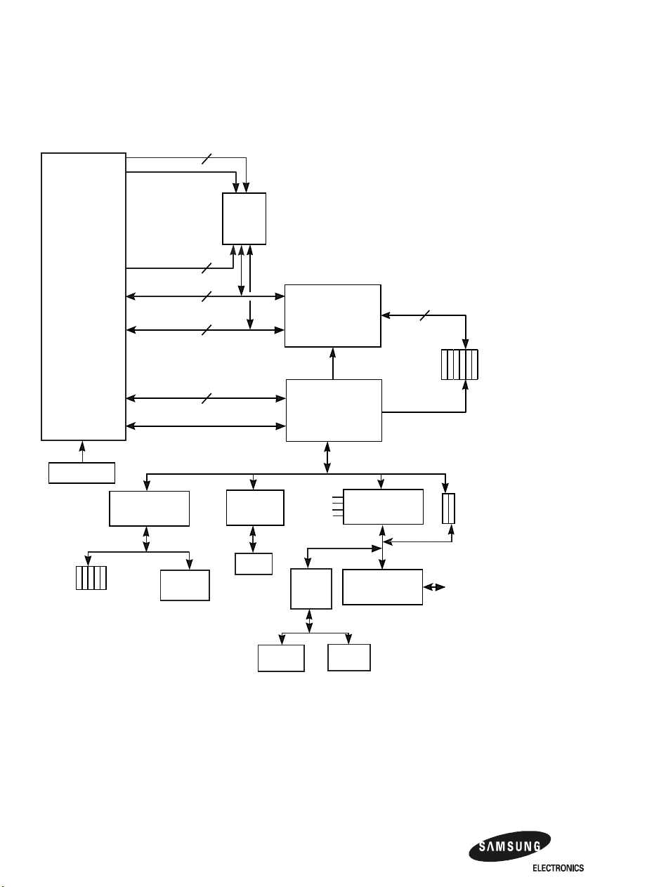
Figure 1-1 shows the board’s functional components.
1
Motherboard
Introduction to the AlphaPC 164UX Motherboard 1–1
Page 16
System Components and Features
Figure 1–1 AlphaPC 164UX Functional Block Diagram
18
2/4MB L3
Bcache
Alpha 21164
Microprocessor
Index
Control
Tag Data
Pdata
Pecc
Address
Commands
Flash ROM
PCI-to-PCI
Bridge
Secondary PCI Bus
5 Dedicated 32-Bit PCI Slots
SCSI
Controller
12
128
16
36
Primary PCI Bus
Ethernet
Controller
SROM
Data Switches
Control
DECchip 21174-CA
Control, I/O Interface,
Buffer
Real Time
Clock
(X5)
and Address
4 Devices
KBD
Controller
PCI-to-ISA
Bridge
Combination
Controller
128-Bit Data
Address/Control
Diskette
Parallel Port
2 Serial Ports
168-Pin
Unbuffered
SDRAM
DIMM
Sockets
(X6)
1 Dedicated 64-Bit PCI Slot
1 Dedicated ISA Slot
1–2 Introduction to the AlphaPC 164UX Motherboard
Page 17
System Components and Features
1.1.1 Digital Semiconductor 21174 Core Logic Chip
The Alpha 21164 microprocessor is supported by the 21174 core logic chip, which
provides an interface between three units—memory, the PCI bus, and the 21164.
This core logic chip is the interface between the 21164 microprocessor, main memory (addressing and control), and the PCI bus.
Five Data switches provide the memory interface data path.
The 21174 includes the majority of functions necessary to develop a high-performance PC or workstation, requiring minimum discrete logic on the module. It provides flexible and generic functions to allow its use in a wide range of systems.
1.1.2 Memory Subsystem
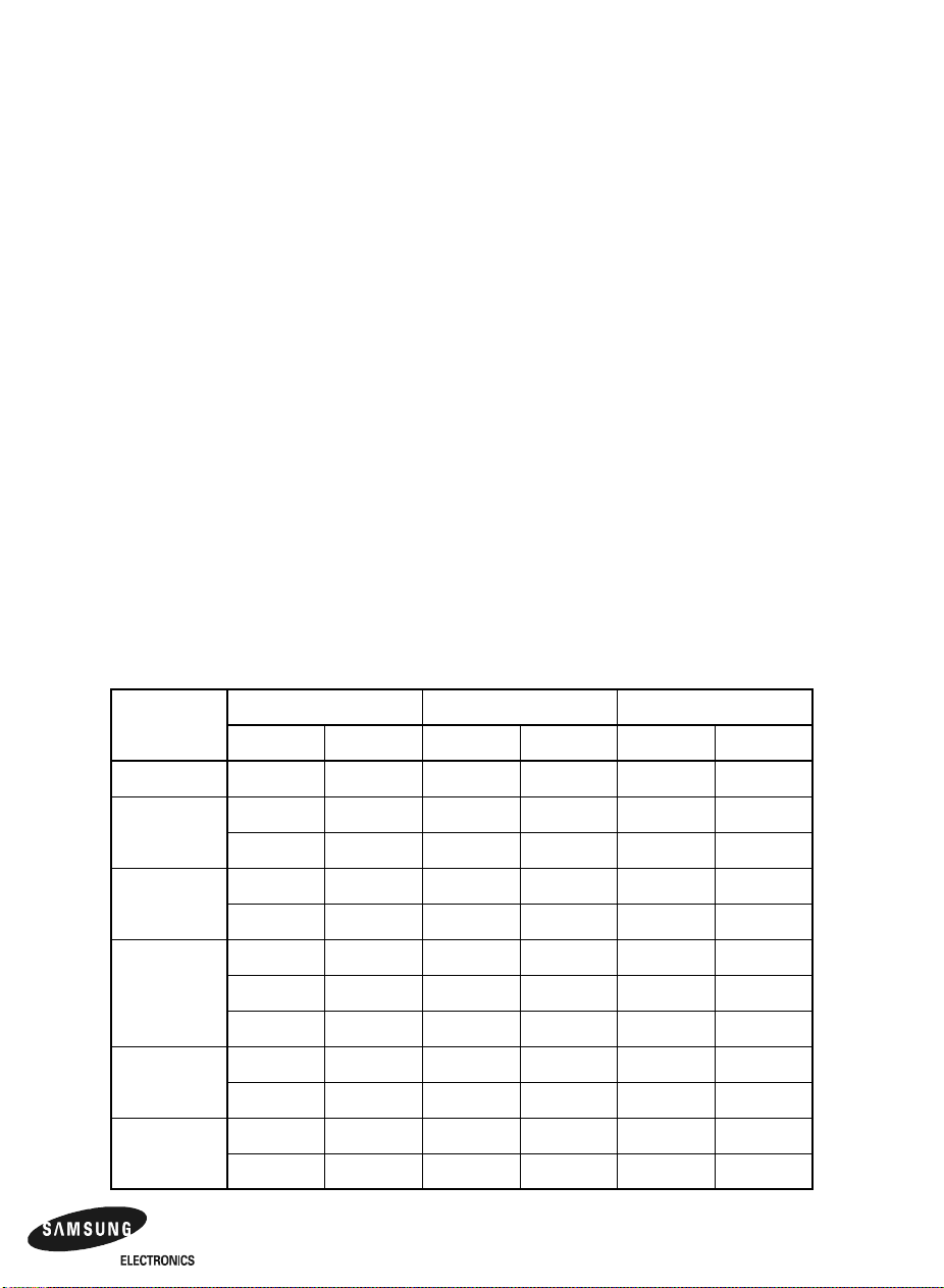
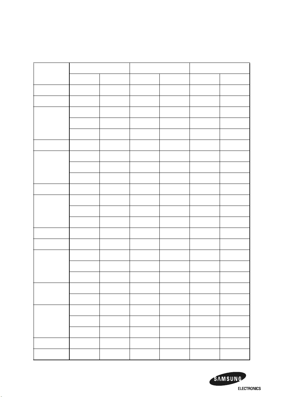
The synchronous dynamic random-access memory (SDRAM) is contained in three
banks of dual inline memory modules (DIMMs). Single- or double-sided DIMMs
may be used. Each DIMM is 72 bits wide, with 64 data bits and 8 check bits, with
100 MHz or faster speed. Two DIMMs provide 32Mb to 512MB of memory, while
six DIMMs provide up to 1536MB. Table 1–1 lists the DIMM sizes tested
Table 1–1 AlphaPC 164UX SDRAM Memory Configurations
Total
Memory
32MB 16MB 16MB
64MB 16MB 16MB 16MB 16MB
96MB 16MB 16MB 16MB 16MB 16MB 16MB
128MB 32MB 32MB 16MB 16MB 16MB 16MB
160MB 32MB 32MB 32MB 32MB 16MB 16MB
192MB 32MB 32MB 32MB 32MB 32MB 32MB
Bank 0 Bank 1 Bank 2
U3 U4 U5 U6 U7 U8
32MB 32MB
32MB 32MB 16MB 16MB
32MB 32MB 32MB 32MB
64MB 64MB
64MB 64MB 16MB 16MB
64MB 64MB 16MB 16MB
Introduction to the AlphaPC 164UX Motherboard 1–3
(Sheet 1 of 3)
Page 18
System Components and Features
Table 1–1 AlphaPC 164UX SDRAM Memory Configurations
Total
Memory
Bank 0 Bank 1 Bank 2
U3 U4 U5 U6 U7 U8
192MB 64MB 64MB 32MB 32MB
224MB 64MB 64MB 32MB 32MB 16MB 16MB
256MB 64MB 64MB 32MB 32MB 32MB 32MB
64MB 64MB 64MB 64MB
128MB 128MB
288MB 128MB 128MB 16MB 16MB
320MB 64MB 64MB 64MB 64MB 32MB 32MB
128MB 128MB 16MB 16MB 16MB 16MB
128MB 128MB 32MB 32MB
352MB 128MB 128MB 32MB 32MB 16MB 16MB
384MB 64MB 64MB 64MB 64MB 64MB 64MB
128MB 128MB 32MB 32MB 32MB 32MB
128MB 128MB 64MB 64MB
416MB 128MB 128MB 64MB 64MB 16MB 16MB
(Sheet 2 of 3)
448MB 128MB 128MB 64MB 64MB 32MB 32MB
512MB 128MB 128MB 64MB 64MB 64MB 64MB
128MB 128MB 128MB 128MB
256MB 256MB
544MB 128MB 128MB 128MB 128MB 16MB 16MB
256MB 256MB 16MB 16MB
576MB 128MB 128MB 128MB 128MB 32MB 32MB
256MB 256MB 16MB 16MB 16MB 16MB
256MB 256MB 32MB 32MB
608MB 256MB 256MB 32MB 32MB 16MB 16MB
640MB 128MB 128MB 128MB 128MB 64MB 64MB
1–4 Introduction to the AlphaPC 164UX Motherboard
Page 19

System Components and Features
Table 1–1 AlphaPC 164UX SDRAM Memory Configurations
Total
Memory
672MB 256MB 256MB 64MB 64MB 16MB 16MB
704MB 256MB 256MB 64MB 64MB 32MB 32MB
768MB 128MB 128MB 128MB 128MB 128MB 128MB
800MB 256MB 256MB 128MB 128MB 16MB 16MB
832MB 256MB 256MB 128MB 128MB 32MB 32MB
896MB 256MB 256MB 128MB 128MB 64MB 64MB
1024MB 256MB 256MB 128MB 128MB 128MB 128MB
1056MB 256MB 256MB 256MB 256MB 16MB 16MB
1088MB 256MB 256MB 256MB 256MB 32MB 32MB
Bank 0 Bank 1 Bank 2
U3 U4 U5 U6 U7 U8
256MB 256MB 32MB 32MB 32MB 32MB
256MB 256MB 64MB 64MB
256MB 256MB 64MB 64MB 64MB 64MB
256MB 256MB 128MB 128MB
256MB 256MB 256MB 256MB
(Sheet 3 of 3)
1152MB 256MB 256MB 256MB 256MB 64MB 64MB
1280MB 256MB 256MB 256MB 256MB 128MB 128MB
1536MB 256MB 256MB 256MB 256MB 256MB 256MB
Note : The following are important items to remember
- in order for the ECC memory feature to work, all DIMMs must be 72bit.
- To populate a bank,you must use 2 matched DIMMs.
1.1.3 L3 Bcache Subsystem Overview
The AlphaPC 164UX board-level L3 backup cache (Bcache) is a 2MB, directmapped, synchronous SRAM with a 128-bit data path. The board is capable of handling an L3 cache size of 4MB. See Section 2.3 for more information about the
Bcache.
Introduction to the AlphaPC 164UX Motherboard 1–5
Page 20

System Components and Features
1.1.4 PCI Interface Overview
The AlphaPC 164UX PCI interface is the main I/O bus for the majority of functions
(SCSI interface, graphics accelerator, and so on). The PCI interface has a 33-MHz
data transfer rate. An onboard PCI-to-ISA bridge is provided through an Intel
82371SB (SIO) chip.An onboard PCI-to-PCI bridge is provided through an DEC
21052 chip.The AlphaPC 164UX includes advanced features,Such as :six PCI
slots;on-board Ultra-Wide SCSI; on-board 10/100 Mbs Ethernet.
1.1.5 ISA Interface Overview
The ISA bus provides the following system support functions:
• One expansion slots.
• An SMC FDC37C666 combination controller chip that provides:
– A diskette controller.
– Two universal asynchronous receiver-transmitters (UARTs) with full
modem control.
– A bidirectional parallel port.
• A mouse and keyboard controller.
• Real Time Clock.
1.1.6 Miscellaneous Logic
The AlphaPC 164UX contains the following miscellaneous components:
• Synthesizer for clocks:
– A clock synthesizer (TQ2061) provides a programmable clock source from
300MHz to 800MHz to the 21164 microprocessor. The microprocessor
supplies a clock to the system PLL/clock buffer for the 21174.
– The 21174 core logic chip provides the SDRAM and PCI clocks.
– 24MHz clock generator provide a clock source for the FDC37C666 ISA
device controller. The controller’s onchip generator then provides other
clocks as needed.
• AMD PALLV22V1015 and PALCE16V8H programmable logic devices (PLDs)
for PCI bus arbitration.
• Altera EPM7032-7 for DMA boundary issue.
1–6 Introduction to the AlphaPC 164UX Motherboard
Page 21

• AMD PALLV22V1015JC for clock controller.
1.2 Software Support
The support elements described in this section are either included with the
AlphaPC 164UX or are available separately.
1.2.1 ARCSBIOS Windows NT Firmware
The AlphaPC 164UX motherboard ships with ARCSBIOS firmware and online documentation that describes how to configure the firmware for Windows NT. This firmware
initializes the system and enables you to install and boot the Windows NT operating
system. The ARCSBIOS firmware resides in the flash ROM on the AlphaPC 164UX
motherboard. Binary images of the ARCSBIOS firmware are included in the Firmware
update diskette, along with a license describing the terms for use and distribution.
1.3 Hardware Design Support
The full design database, including schematics and source files, is supplied. User
documentation is also included. The database allows designers with no previous
Alpha architecture experience to successfully develop a working Alpha system with
minimal assistance.
Software Support
Introduction to the AlphaPC 164UX Motherboard 1–7
Page 22

2
System Configuration and Connectors
This chapter describes the AlphaPC 164UX configuration, board connectors and
functions, and jumper functions. It also identifies jumper and connector locations.
The AlphaPC 164UX uses jumpers to implement configuration parameters such as
system speed and boot parameters. These jumpers must be configured for the user’s
environment. Onboard connectors are provided for the I/O interfaces, DIMMs, and
serial and parallel peripheral ports.
Figure 2–1 shows the board outlines and identifies the location of jumpers, connectors, and major components. Table 2–1 lists and defines these items.
System Configuration and Connectors 2–1
Page 23
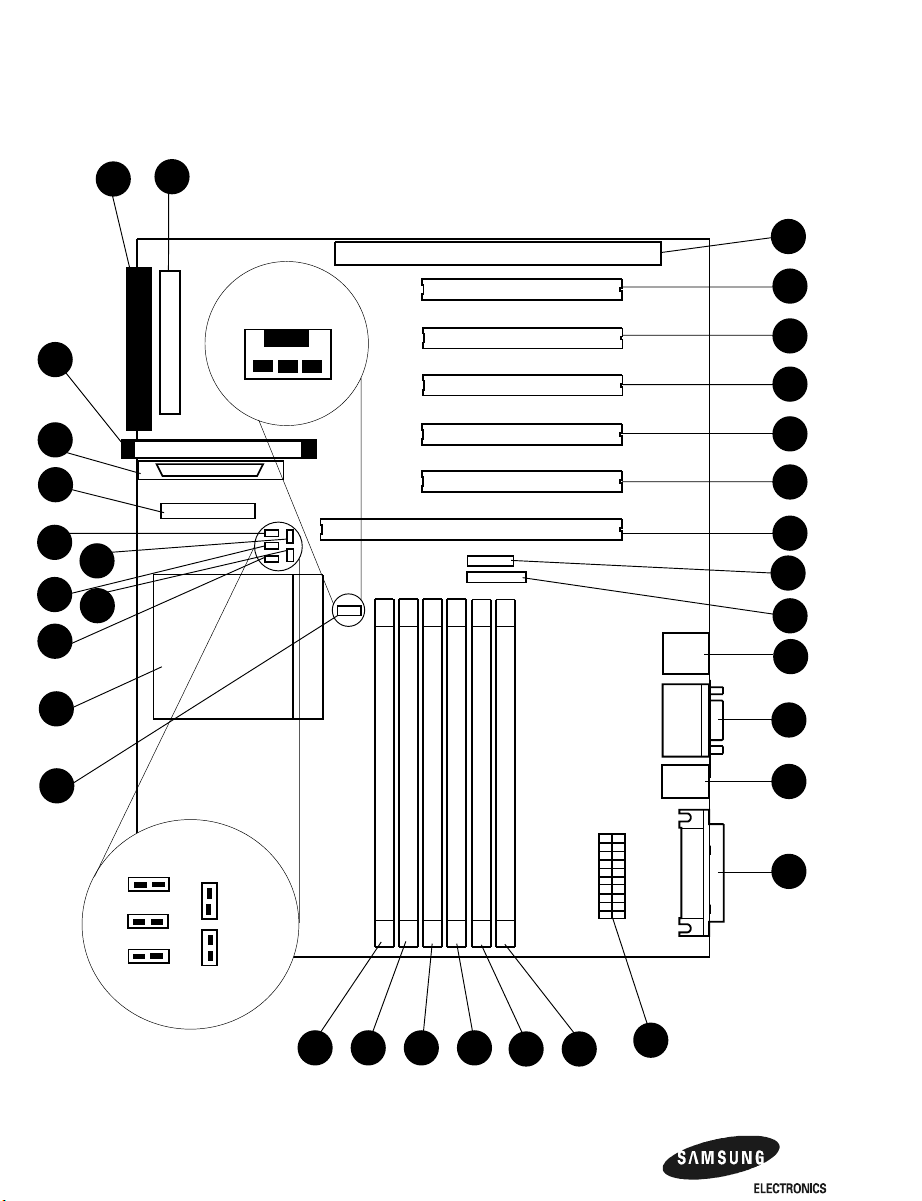
Figure 2–1 AlphaPC 164UX Jumper/Connector Location
J24
J33
J10
J16
J15
J28
J30
J29
J17
U55
J35
J36
J37
Blk
wire
GND
Yellow
wire
FOK
+12
Red
wire
J22
J21
J7
J6
J5
J2
J23
J31
J34
J12
J25
Pwr LED
IDE LED
SCSI LED
Pwr
Switch
Reset
Switch
2–2 System Configuration and Connectors
J13
U5U6U7U8
U3U4
J18
Page 24
AlphaPC 164UX Jumper Configuration
Table 2–1 AlphaPC 164UX Jumper/Connector List
Item
No. Description
J2 Full length 64 bit PCI slot U3 DIMM socket 0
J5 Half length 32 bit PCI slot U4 DIMM socket 1
J6 Full length 32 bit PCI slot U5 DIMM socket 2
J7 Full length 32 bit PCI slot U6 DIMM socket 3
J10 Full length ISA slot U7 DIMM socket 4
J12 Serial Port connector U8 DIMM socket 5
J13 Parallel port connector U55 Microprocessor socket(21164 Alpha)
J15 Ultra Fast and Wide SCSI Connector
J16 Narrow SCSI connector
J17 SCSI LED connector
J18 Power connector
J21 Full length 32 bit PCI slot
J22 Full length 32 bit PCI slot
J23 Speaker connector
J24 IDE drive connector
J25 Keyboard/Mouse connector
J28 Configuration jumpers
J29 IDE LED connector
J30 2 pin Power LED connector
J31 5 pin Power LED connector
J33 Floppy drive connector
J34 10/100 Mbit ethernet connector
J35 Microprocessor fan/fan sense connector
J36 Power switch connector
J37 Reset switch connector
Item
No. Description
2.1 AlphaPC 164UX Jumper Configuration
The AlphaPC 164UX has one set of jumpers located at J28. These jumpers set the
hardware configuration and boot options. Figure 2–1 shows the jumper location on
the AlphaPC 164UX motherboard. Figure 2–2 shows the jumper functions for each
group.
System Configuration and Connectors 2–3
Page 25
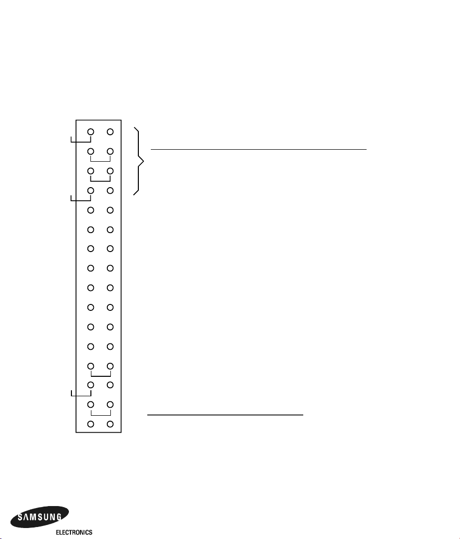
Figure 2–2 AlphaPC 164UX Configuration Jumpers
)
J28 System Configuration Jumpers
Option 1
Option 2
Option 3
Option 4
Option 5
Option 6
Frequency
300 MHz In In In In
333 MHz
366 MHz
400 MHz Out Out In In
433 MHz
466 MHz
500 MHz In Out Out In
533 MHz
566 MHz
Option1 Option2 Option3 Option4
Out
In
In
Out
Out
In
600 MHz Out In In Out
Option 7
Option 8
Option 9
Option 10
Option 11
Option 12
Option 13
Option 14
Option 15
Option 16
633 MHz
666 MHz
700 MHz In In Out Out
733 MHz
766 MHz
800 MHz Out Out Out Out
Option 5 : Pyxis Bus Speed Select(Default Out)
Option 6 : Reserved Default Out
Option 7 : Enable SROM Debug Mode(Default Out)
Option 8 : Enable Firmware Debug Mode(Default Out)
Option 9 : Enable only 1 set of Scache(Default Out)
Option 10 : Reserved Default Out
Option 11 : Boot SAFE ARCSBIOS Image(Default Out)
Option 12 : Reserved Default Out
Option 13 : Must be In
Bcache Size
0MB
1MB
2MB
4MB
In
Out
Out
In
Option14 Option15
In
In
Out
Out
In In In
Out In In
In Out In
In Out In
Out Out In
In In Out
Out In Out
Out In Out
In Out Out
Out Out Out
Out
In
Out
In
Option 16 : FAN OK Signal Do not ever populate(Default Out
System Configuration and Connectors 2–4
Page 26

CPU Speed Selection (Option 1,2,3, &4)
2.2 CPU Speed Selection (Option 1,2,3, &4)
The clock synthesizer makes it possible to change the frequency of the microprocessor’s clock input without having to change the clock crystal. Simply set the speed
jumpers to adjust the frequency of the microprocessor’s clock. These speed jumpers
are located at J28-1/2 (Option 1), J28-3/4 (Option 2), J28-5/6 (Option 3), and J28-7/8
(Option 4). These four jumpers set speed at power-up as listed in Figure 2–2.
2.3 Bcache Size Jumpers (Option 14,15)
The Bcache size jumpers are located at J28–27/28 (Option14) and J28–29/30
(Option15), as shown in Figure 2–2. The AlphaPC 164UX-2/-4 is configured with
2MB/4MB of Bcache during production ; the other jumpers shown in Figure 2–2
(0,1) are for other implementations.
Note: The standard motherboard is manufactured with 128K X 18 or 256K X
18 data SSRAMs.
2.4 Boot Option Jumper (Option 11)
The boot option jumper is located at J28-21/22 (Option 11). The default position for
this jumper is out (Figure 2–2). This jumper selects the image to be loaded into memory from the system flash ROM. With the jumper out the ARCSBIOS firmware is
loaded. With the jumper in, the Safe ARCSBIOS is loaded.
2.5 AlphaPC 164UX Connector Pinouts
This section lists the pinouts of all AlphaPC 164UX connectors. See Figure 2–1 for
connector locations.
2.5.1 PCI Bus Connector Pinouts
Table 2–2 shows the PCI bus connector pinouts.
Table 2–2 PCI Bus Connector Pinouts
Pin Signal Pin Signal Pin Signal Pin Signal
32-Bit and 64-Bit PCI Connectors (J2, J5, J6, J7, J21, J22)
A1 TRST# A2 +12V A3 TMS A4 TDI
A5 Vdd A6 INTA A7 INTC A8 Vdd
System Configuration and Connectors 2–5
(Sheet 1 of 3)
Page 27

AlphaPC 164UX Connector Pinouts
Table 2–2 PCI Bus Connector Pinouts
Pin Signal Pin Signal Pin Signal Pin Signal
(Sheet 2 of 3)
A9 —A10Vdd A11 — A12 Gnd
A13 Gnd A14 — A15 RST# A16 Vdd
A17 GNT# A18 Gnd A19 — A20 AD<30>
A21 +3V A22 AD<28> A23 AD<26> A24 Gnd
A25 AD<24> A26 IDSEL A27 +3V A28 AD<22>
A29 AD<20> A30 Gnd A31 AD<18> A32 AD<16>
A33 +3V A34 FRAME# A35 Gnd A36 TRDY#
A37 STOP# A38 STOP# A39 +3V A40 SDONE
A41 SBO# A42 Gnd A43 PA R A44 AD<15>
A45 +3V A46 AD<13> A47 AD<11> A48 Gnd
A49 AD<09> A50 Not used A51 Not used A52 C/BE#<0>
A53 +3V A54 AD<06> A55 AD<04> A56 Gnd
A57 AD<02> A58 AD<00> A59 Vdd A60 REQ64#
A61 Vdd A62 Vdd B1 –12V B2 TCK
B3 Gnd B4 TDO B5 Vdd B6 Vdd
B7 INTB B8 INTD B9 PRSNT1# B10 —
B11 PRSNT2# B12 Gnd B13 Gnd B14 —
B15 Gnd B16 CLK B17 Gnd B18 REQ#
B19 Vdd B20 AD<31> B21 AD<29> B22 Gnd
B23 AD<27> B24 AD<25> B25 +3V B26 C/BE#<3>
B27 AD<23> B28 Gnd B29 AD<21> B30 AD<19>
B31 +3V B32 AD<17> B33 C/BE#<2> B34 Gnd
B35 IRDY# B36 +3V B37 DEVSEL# B38 Gnd
B39 LOCK# B40 PERR# B41 +3V B42 SERR#
B43 +3V B44 C/BE#<1> B45 AD<14> B46 Gnd
B47 AD<12> B48 AD<10> B49 Gnd B50 Not used
B51 Not used B52 AD<08> B53 AD<07> B54 +3V
B55 AD<05> B56 AD<03> B57 Gnd B58 AD<01>
B59 Vdd B60 ACK64# B61 Vdd B62 Vdd
64-Bit PCI Connectors Only (J2)
A63 Gnd A64 C/BE#<7> A65 C/BE#<5> A66 Vdd
A67 PA R64 A68 D<62> A69 Gnd A70 D<60>
A71 D<58> A72 Gnd A73 D<56> A74 D<54>
A75 Vdd A76 D<52> A77 D<50> A78 Gnd
A79 D<48> A80 D<46> A81 Gnd A82 D<44>
2–6 System Configuration and Connectors
Page 28

AlphaPC 164UX Connector Pinouts
Table 2–2 PCI Bus Connector Pinouts
Pin Signal Pin Signal Pin Signal Pin Signal
A83 D<42> A84 Vdd A85 D<40> A86 D<38>
A87 Gnd A88 D<36> A89 D<34> A90 Gnd
A91 D<32> A92 —A93Gnd A94 —
B63 — B64 Gnd B65 C/BE#<6> B66 C/BE#<4>
B67 Gnd B68 D<63> B69 D<61> B70 Vdd
B71 D<59> B72 D<57> B73 Gnd B74 D<55>
B75 D<53> B76 Gnd B77 D<51> B78 D<49>
B79 Vdd B80 D<47> B81 D<45> B82 Gnd
B83 D<43> B84 D<41> B85 Gnd B86 D<39>
B87 D<37> B88 Vdd B89 D<35> B90 D<33>
B91 Gnd B92 — B93 — B94 Gnd
(Sheet 3 of 3)
System Configuration and Connectors 2–7
Page 29

AlphaPC 164UX Connector Pinouts
2.5.2 ISA Expansion Bus Connector Pinouts
Table 2–3 shows the ISA expansion bus connector pinouts.
Table 2–3 ISA Expansion Bus Connector Pinouts (J10)
Pin Signal Pin Signal Pin Signal Pin Signal
1 Gnd 2 IOCHCK# 3 RSTDRV 4 SD7
5 Vdd 6 SD6 7 IRQ9 8 SD5
9 –5V 10 SD4 11 DRQ2 12 SD3
13 –12V 14 SD2 15 ZEROWS# 16 SD1
17 +12V 18 SD0 19 Gnd 20 IOCHRDY
21 SMEMW# 22 AEN 23 SMEMR# 24 SA19
25 IOW# 26 SA18 27 IOR# 28 SA17
29 DACK3# 30 SA16 31 DRQ3 32 SA15
33 DACK1# 34 SA14 35 DRQ1 36 SA13
37 REFRESH# 38 SA12 39 SYSCLK 40 SA11
41 IRQ7 42 SA10 43 IRQ6 44 SA9
45 IRQ5 46 SA8 47 IRQ4 48 SA7
49 IRQ3 50 SA6 51 DACK2# 52 SA5
53 TC 54 SA4 55 BALE 56 SA3
57 Vdd 58 SA2 59 OSC 60 SA1
61 Gnd 62 SA0 63 MEMCS16# 64 SBHE#
65 IOCS16# 66 LA23 67 IRQ10 68 LA22
69 IRQ11 70 LA21 71 IRQ12 72 LA20
73 IRQ15 74 LA19 75 IRQ14 76 LA18
77 DACK0# 78 LA17 79 DRQ0 80 MEMR#
81 DACK5# 82 MEMW# 83 DRQ5 84 SD8
85 DACK6# 86 SD9 87 DRQ6 88 SD10
89 DACK7# 90 SD11 91 DRQ7 92 SD12
93 Vdd 94 SD13 95 MASTER# 96 SD14
97 Gnd 98 SD15 —— ——
2–8 System Configuration and Connectors
Page 30

2.5.3 SDRAM DIMM Connector Pinouts
Table 2–4 shows the SDRAM DIMM connector pinouts.
AlphaPC 164UX Connector Pinouts
Table 2–4 SDRAM DIMM Connector Pinouts (U3 through U8)1
Pin Signal Pin Signal Pin Signal Pin Signal
1 Gnd 2 DQ0 3 DQ1 4 DQ2
5 DQ3 6 3.3V 7 DQ4 8 DQ5
9 DQ6 10 DQ7 11 DQ8 12 Gnd
13 DQ9 14 DQ10 15 DQ11 16 DQ12
17 DQ13 18 3.3V 19 DQ14 20 DQ15
21 CB0 22 CB1 23 Gnd 24 NC
25 NC 26 3.3V 27 WE
29 DQMB1 30 S0
33 A0 34 A2 35 A4 36 A6
37 A8 38 A10 39 A12 40 3.3V
41 3.3V 42 CK0 43 Gnd 44 NC
45 S2
49 3.3V 50 NC 51 NC 52 CB2
53 CB3 54 Gnd 55 DQ16 56 DQ17
57 DQ18 58 DQ19 59 3.3V 60 DQ20
61 NC 62 NC 63 CKE1 64 Gnd
65 DQ21 66 DQ22 67 DQ23 68 Gnd
69 DQ24 70 DQ25 71 DQ26 72 DQ27
73 3.3V 74 DQ28 75 DQ29 76 DQ30
77 DQ31 78 Gnd 79 CK2 80 NC
81 NC 82 SDA 83 SCL 84 3.3V
85 Gnd 86 DQ32 87 DQ33 88 DQ34
89 DQ35 90 3.3V 91 DQ36 92 DQ37
93 DQ38 94 DQ39 95 DQ40 96 Gnd
97 DQ41 98 DQ42 99 DQ43 100 DQ44
101 DQ45 102 3.3V 103 DQ46 104 DQ47
105 CB4 106 CB5 107 Gnd 108 NC
109 NC 110 3.3V 111 CAS
113 DQMB5 114 S1 115 RAS
117 A1 118 A3 119 A5 120 A7
121 A9 122 BA0 123 A13 124 3.3V
46 DQMB2 47 DQMB3 48 NC
31 NC 32 Gnd
28 DQMB0
112 DQMB4
116 Gnd
(Sheet 1 of 2)
System Configuration and Connectors 2–9
Page 31

AlphaPC 164UX Connector Pinouts
1
Table 2–4 SDRAM DIMM Connector Pinouts (U3 through U8)
Pin Signal Pin Signal Pin Signal Pin Signal
125 CK1 126 BA1
129 S3
130 DQMB6 131 DQMB7 132 PD
2
127 Gnd 128 CKE0
(Sheet 2 of 2)
3
133 3.3V 134 NC 135 NC 136 CB6
137 CB7 138 Gnd 139 DQ48 140 DQ49
141 DQ50 142 DQ51 143 3.3V 144 DQ52
145 NC 146 NC 147 PD 148 Gnd
149 DQ53 150 DQ54 151 DQ55 152 Gnd
153 DQ56 154 DQ57 155 DQ58 156 DQ59
157 3.3V 158 DQ60 159 DQ61 160 DQ62
161 DQ63 162 Gnd 163 CK3 164 NC
165 SA0 166 SA1 167 SA2 168 3.3V
1
Pins 1 through 84 are on the front side and pins 85 through 168 are on the back side.
2
The AlphaPC 164UX uses BA1 as both BA1 and ADDR12. Therefore, four-bank DIMMs using
ADDR<11:0> are the maximum size. (Two-bank DIMMs can use ADDR<12:0>.)
3
Pull-down.
2.5.4 EIDE Drive Bus Connector Pinouts
Table 2–5 shows the EIDE drive bus connector pinouts.
Table 2–5 EIDE Drive Bus Connector Pinouts (J24)
Pin Signal Pin Signal Pin Signal Pin Signal
1 RESET
5 IDE_D6 6 IDE_D9 7 IDE_D5 8 IDE_D10
9 IDE_D4 10 IDE_D11 11 IDE_D3 12 IDE_D12
13 IDE_D2 14 IDE_D13 15 IDE_D1 16 IDE_D14
17 IDE_D0 18 IDE_D15 19 Gnd 20 NC (key pin)
21 MARQ 22 Gnd 23 IOW
25 IOR
29 MACK 30 Gnd 31 IRQ 32 IOCS16
33 ADDR1 34 NC 35 ADDR0 36 ADDR2
37 CS0
2 Gnd 3 IDE_D7 4 IDE_D8
24 Gnd
26 Gnd 27 CHRDY 28 BALE
38 CS1 39 ACT 40 Gnd
2–10 System Configuration and Connectors
Page 32

AlphaPC 164UX Connector Pinouts
2.5.5 Diskette Drive Bus Connector Pinouts
Table 2–6 shows the diskette (floppy) drive bus connector pinouts.
Table 2–6 Diskette (Floppy) Drive Bus Connector Pinouts (J33)
Pin Signal Pin Signal Pin Signal Pin Signal
1 Gnd 2 DEN0 3 Gnd 4NC
5Gnd 6 DEN1 7 Gnd 8 INDEX
9 Gnd 10 MTR0 11 Gnd 12 DR1
13 Gnd 14 DR0 15 Gnd 16 MTR1
17 Gnd 18 DIR 19 Gnd 20 STEP
21 Gnd 22 WDATA 23 Gnd 24 WGATE
25 Gnd 26 TRK0 27 Gnd 28 WRTPRT
29 ID0 30 RDATA 31 Gnd 32 HDSEL
33 ID1 34 DSKCHG —— — —
2.5.6 Parallel Bus Connector Pinouts
Table 2–7 shows the parallel bus connector pinouts.
Table 2–7 Parallel Bus Connector Pinouts (J13)
Pin Signal Pin Signal Pin Signal Pin Signal
1 STB 2 PD0 3 PD1 4 PD2
5 PD3 6 PD4 7 PD5 8 PD6
9 PD7 10 ACK 11 BUSY 12 PE
13 SLCT 14 AFD 15 ERR 16 INIT
17 SLIN 18 Gnd 19 Gnd 20 Gnd
21 Gnd 22 Gnd 23 Gnd 24 Gnd
25 Gnd —— —— — —
System Configuration and Connectors 2–11
Page 33

AlphaPC 164UX Connector Pinouts
2.5.7 COM1/COM2 Serial Line Connector Pinouts
Table 2–8 shows the COM1/COM2 serial line connector pinouts.
Table 2–8 COM1/COM2 Serial Line Connector Pinouts (J12)
COM1 Pin
(Top) COM1 Signal
1 DCD1 1 DCD2
2 RxD1 2 RxD2
3 TxD1 3 TxD2
4 DTR1 4 DTR2
5 SG1 5 SG2
6 DSR1 6 DSR2
7 RTS1 7 RTS2
8 CTS1 8 CTS2
9 RI1 9 RI2
COM2 Pin
(Bottom) COM2 Signal
2.5.8 Keyboard/Mouse Connector Pinouts
Table 2–9 shows the keyboard/mouse connector pinouts.
Table 2–9 Keyboard/Mouse Connector Pinouts (J25)
Keyboard Pin
(Bottom) Keyboard Signal
1 KBDATA 1 MSDATA
2NC 2NC
3Gnd 3 Gnd
4 Vdd 4 Vdd
5 KBCLK 5 MSCLK
6NC 6NC
2–12 System Configuration and Connectors
Mouse Pin
(Top) Mouse Signal
Page 34
2.5.9 Input Power Connector Pinouts
Table 2–10 shows the input power connector pinouts.
AlphaPC 164UX Connector Pinouts
Table 2–10 Input Power Connector Pinouts (J18)
Pin Voltage Pin Voltage Pin Voltage Pin Voltage
1 +3.3 V dc 2 +3.3 V dc 3 Gnd 4 +5 V dc
5 Gnd 6 +5 V dc 7 Gnd 8 P_DCOK
9 5 V SB 10 +12 V dc 11 +3.3 V dc 12 –12 V dc
13 Gnd 14 PS_ON 15 Gnd 16 Gnd
17 Gnd 18 –5 V dc 19 +5 V dc 20 +5 V dc
1
This pinout is ATX-compliant.
2.5.10 Narrow SCSI Bus Connector
Table 2-11 shows the narrow SCSI bus connector pinouts
Table 2–11 Narrow SCSI Bus Connector (J16)
Pin Signal Pin Signal Pin Signal Pin Signal
1 GND 2 SD0
5 GND 6 SD2 7 GND 8 SD3
9 GND 10 SD4 11 GND 12 SD5
13 GND 14 SD6 15 GND 16 SD7
17 GND 18 SDPO 19 GND 20 GND
21 GND 22 BUS_PRES 23 GND 24 GND
25 NC 26 TERMPWR 27 GND 28 GND
29 GND 30 GND 31 GND 32 SATN
33 GND 34 GND 35 GND 36 SBSY
37 GND 38 SACK 39 GND 40 SRST
41 GND 42 SMSG 43 GND 44 SSEL
45 GND 46 SCD 47 GND 48 SREQ
49 GND 50 SIO
1
3 GND 4 SD1
System Configuration and Connectors 2–13
Page 35
AlphaPC 164UX Connector Pinouts
2.5.11 Fast and Wide SCSI Bus Connector
Table 2–12 shows the Fast and Wide SCSI bus connector pinouts
Table 2–12 Fast and Wide SCSI Connector Pinouts (J15)
Pin Signal Pin Signal Pin Signal Pin Signal
1 GND 2 GND 3 GND 4 GND
5 GND 6 GND 7 GND 8 GND
9 GND 10 GND 11 GND 12 GND
13 GND 14 GND 15 GND 16 GND
17 TERMPWR1 18 TERMPWR1 19 NC 20 GND
21 GND 22 GND 23 GND 24 GND
25 GND 26 GND 27 GND 28 GND
29 GND 30 GND 31 GND 32 GND
33 GND 34 GND 35 SD12
37 SD14 38 SD15 39 SDP1 40 SD0
41 SD1 42 SD2 43 SD3 44 SD4
45 SD5 46 SD6 47 SD7 48 SDP0
49 GND 50 BUS_PRES 51 TERMPWR1 52 TERMPWR1
53 NC 54 GND 55 SATN
57 SBSY
61 SSEL 62 SCD 63 SREQ 64 SIO
65 SD8 66 SD9 67 SD10 68 SD11
69 GND 70 GND
58 SACK 59 SRST 60 SMSG
36 SD13
56 GND
2.5.12 10/100 Mbit Ethernet Connector Pinouts
Table 2–13 shows the Fast and Wide SCSI bus connector pinouts.
Table 2–13 10/100 Mbit Ethernet Connector Pinouts (34)
Pin Signal Pin Signal Pin Signal Pin Signal
1 TD_P 2 TD_M 3 RD_P 4 U1
5U2 6RD_M 7U3 8U4
9MP1 10MP2
2–14 System Configuration and Connectors
Page 36

AlphaPC 164UX Connector Pinouts
2.5.13 Speaker Connector Pinouts
Table 2–14 shows the speaker connector pinouts.
Table 2–14 Speaker Connector Pinouts (J23)
Pin Signal Name
1 SPKR Speaker output
2 NC —
3 VDD —
4 GND —
2.5.14 Microprocessor Fan Power Connector Pinouts
Table 2–15 shows the microprocessor fan power connector pinouts.
Table 2–15 Microprocessor Fan Power Connector Pinouts (J35)
Pin Signal Name
1 +12V —
2 FAN_OK_L Fan connected
3 GND —
2.5.15 Pin Power LED Connector Pinouts
Table 2–16 shows the power LED connector pinouts.
Table 2–16 Power LED Connector Pinouts (J31)
Pin Signal Name
1 Powerpullup Power pullup
2NC —
3 GND —
4NC —
5NC —
System Configuration and Connectors 2–15
Page 37

AlphaPC 164UX Connector Pinouts
2.5.16 IDE Drive LED Connector Pinouts
Table 2–17 shows the IDE drive LED connector pinouts.
Table 2–17 IDE Drive LED Connector Pinouts (J29)
Pin Signal Name
1 ACTIVITY
2 ACTIVUTYPULLUP
Hard drive active
2.5.17 Reset Switch Connector Pinouts
Table 2–18 shows the reset switch connector pinouts.
Table 2–18 Reset Switch Connector Pinouts (J37)
Pin Signal Name
1 GND —
2 RSTSWITCH
Reset system
2.5.18 Soft Power Switch Connector Pinouts
Table 2–19 shows the soft power switch connector pinouts.
Table 2–19 Soft Power Switch Connector Pinouts (J36)
Pin Signal Name
1 GND —
2 PWRSWITCH
System power on/off
2.5.19 SCSI LED Connector Pinouts
Table 2–20 shows the SCSI LED connector pinouts.
Table 2–20 SCSI LED Connector Pinouts (J17)
Pin Signal Name
1 SCSI_BUSY
2 SCSI_BSY2
2–16 System Configuration and Connectors
—
—
Page 38

3
Functional Description
This chapter describes the functional operation of the AlphaPC 164UX. The description introduces the Digital Semiconductor 21174 core logic chip and describes its
implementation with the 21164 microprocessor, its supporting memory, and I/O
devices. Figure 1–1 shows the AlphaPC 164UX major functional components.
Bus timing and protocol information found in other data sheets and reference documentation is not duplicated. See Appendix C for a list of supporting documents and
order numbers.
Note: For detailed descriptions of bus transactions, chip logic, and operation,
refer to the 21164 Alpha Microprocessor Hardware Reference Manual
and the Digital Semiconductor 21174 Core Logic Chip Technical Refer-
ence Manual. For details of the PCI interface, refer to the PCI System
Design Guide.
Functional Description 3–1
Page 39
AlphaPC 164UX Bcache Interface
3.1 AlphaPC 164UX Bcache Interface
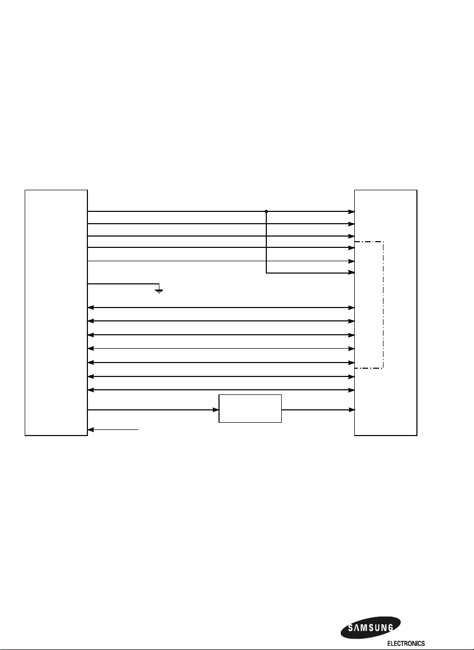
The 21164 microprocessor controls the board-level L3 backup cache (Bcache) array
(see Figure 3–1). The data bus (pdata<127:0>), check bus (pecc<15:0>),
p_tag_dirty and p_tag_ctl_par signals are shared with the system interface.
Figure 3–1 AlphaPC 164UX L3 Bcache Array
21164
Microprocessor
pc164ux.1-2
tag_data<38:32>
tag_data<31:20>
tag_data_par
tag_ctl_par
tag_valid
tag_dirty
pdata<127:0>
pecc<15:0>
untermstclk1
idle_bc
(From 21174 Chip)
CDC2351
pc164ux.4
index<21:4>
*cacheoe
*cachewe
*tag_ram_oe
*tag_ram_we
index<21:6>
Tag
Array
stclk<9:1>
The Bcache is a 2MB or 4MB, direct-mapped, synchronous SRAM (SSRAM)
with a 128-bit data path. It is populated with a quantity of eight 128K
256K x 18 SSRAMs for data store, and one 64K X 18 SSRAM for the tag store.
In most cases, wave-pipelined accesses can decrease the cache loop times by
one CPU cycle. The Bcache supports 64-byte transfers to and from memory.
Bcache
SRAM
Data
Array
pc164ux.5-6
X 18 or
3.2 Digital Semiconductor 21174 Core Logic Chip
The 21174 core logic chip provides a cost-competitive solution for designers using the
21164 microprocessor to develop uniprocessor systems. The chip provides a 128-bit
memory interface and a PCI I/O interface, and includes the Digital Semiconductor
21174-CA chip packaged in a 474-pin plastic ball grid array (PBGA).
3–2 Functional Description
Page 40
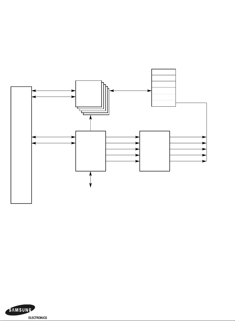
Figure 3–2 shows the AlphaPC 164UX implementation of the 21174 core logic chip.
Figure 3–2 Main Memory Interface
21164
pdata<127:0>
pecc<15:0>
Switches
pc164ux.11
Digital Semiconductor 21174 Core Logic Chip
DIMM 0
DIMM 1
Data
(X5)
enabledataswitch<0:2>
mdata<128:0>
mecc<15:0>
DIMM 2
DIMM 3
DIMM 4
DIMM 5
pc164ux.12-14
paddr<39:4>
*System Control
* addr_bus_req
adr_cmd_par
cack
cmd<3:0>
dack
fill
fill_error
fill_id
idle_bc
int4_valid<3:0>
sys_res<1:0>
tag_ctl_par
pc164ux.1-2
tag_dirty
victim_pending
3.2.1 21174 Chip Overview
The 21174 application-specific integrated circuit (ASIC) accepts addresses and commands from the 21164 microprocessor and drives the main memory array with the
address, control, and clock signals. It also provides an interface to the 64-bit PCI I/O
bus.
The 21174 chip provides the following functions:
• Serves as the interface between the 21164 microprocessor, main memory
(addressing and control), and the PCI bus. A three-entry CPU instruction queue
is implemented to capture commands should the memory or I/O port be busy.
21174
pc164ux.8-10
64-Bit PCI
I/O Bus
dram_addr<13:0>
*we
*cas
*ras
miscellaneous
Buffers
pc164ux.15-17
buf_addr<13:0>
*buf_we<5:0>
*buf_cas<5:0>
*buf_ras<5:0>
buf_miscellaneous
• Provides control to the Data Switch chips to isolate the L3 cache from the main
memory bus during private reads and writes.
Functional Description 3–3
Page 41

Digital Semiconductor 21174 Core Logic Chip
• Generates the clocks, row, and column addresses for the SDRAM DIMMs, as
well as all of the memory control signals (*RAS,*CAS, *WE). All of the
required SDRAM refresh control is contained in the 21174.
• Provides all the logic to map 21164 noncacheable addresses to PCI address
space, as well as all the translation logic to map PCI DMA addresses to system
memory.
Two DMA conversion methods are supported:
• Direct mapping, in which a base offset is concatenated with the PCI address.
• Scatter-gather mapping, which maps an 8KB PCI page to any 8KB memory
page. The 21174 contains an eight-entry scatter-gather translation lookaside
buffer (TLB), where each entry holds four consecutive page table entries (PTEs).
Refer to Appendix A for additional details on PCI and DMA address mapping.
3.2.2 Main Memory Interface
Five Data Switches provide the interface between the 21164/L3 cache (pdata<127:0>,
pecc<15:0>) and the memory/21174 (mdata<127:>, mecc<15:0>). The AlphaPC
164UX supports six168-pin unbuffered 72-bit SDRAM DIMM modules. Quadword
ECC is supported on the SDRAM and CPU buses. Even parity is generated on the PCI
bus.
The AlphaPC 164UX supports a maximum of 1536MB of main memory. The memory is organized as three banks. Table 1–1 lists total memory options along with the
corresponding DIMM sizes required. All CPU cacheable memory accesses and PCI
DMA accesses are controlled and routed to main memory by the 21174 core logic
chip.
The AlphaPC 164UX implements the alternate memory mode for SDRAM RAS
and CAS control signals. Alternate memory mode is explained in the Digital
Semiconductor 21174 Core Logic Chip Technical Reference Manual.
3.2.3 PCI Devices
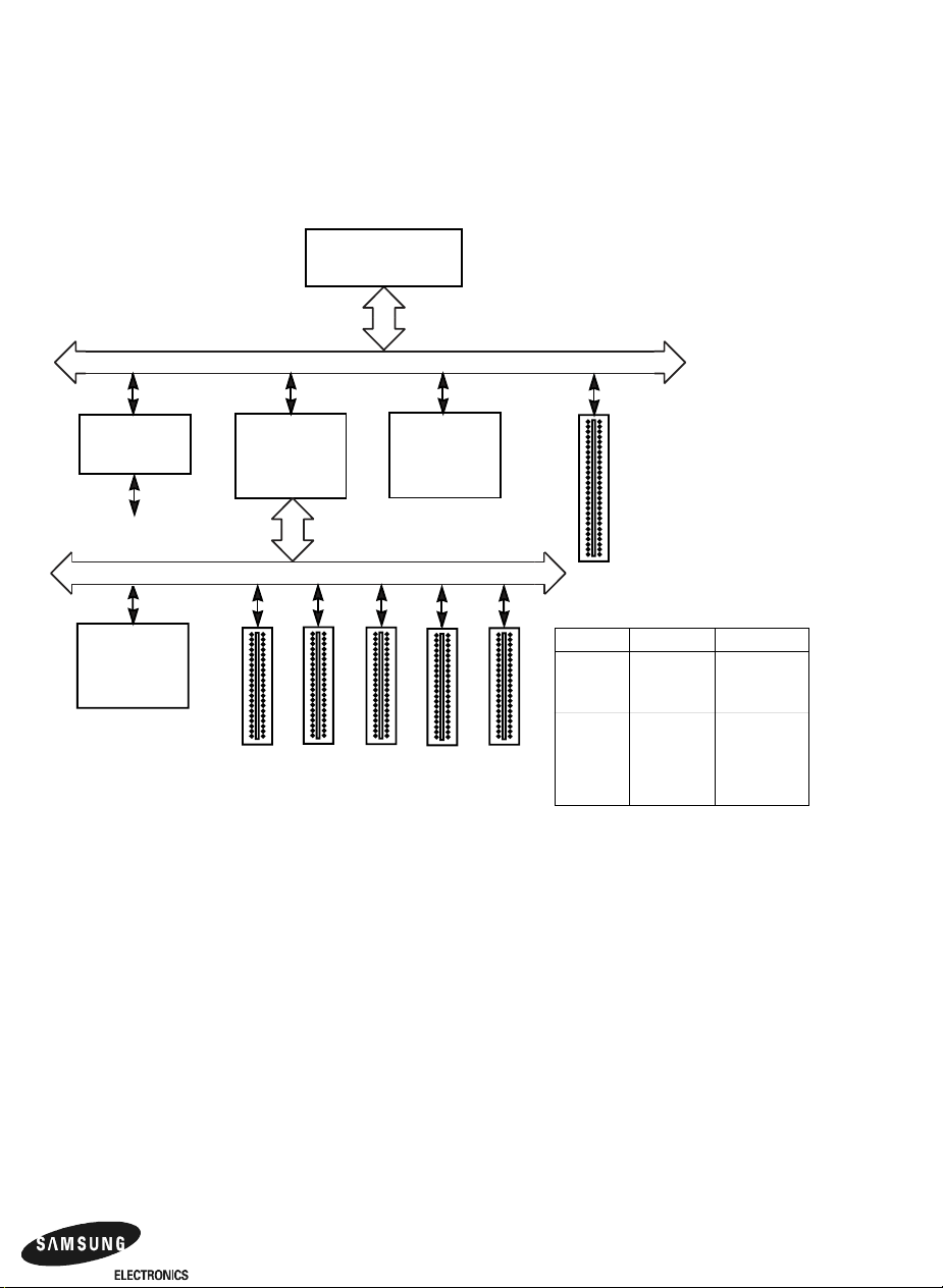
The AlphaPC 164UX uses the PCI bus as the main I/O bus for the majority of
peripheral functions. As Figure 3–3 shows, the board implements the ISA bus as an
expansion bus for system support functions and for relatively slow peripheral
devices.
3–4 Functional Description
Page 42
Digital Semiconductor 21174 Core Logic Chip
Figure 3–3 AlphaPC 164UX PCI Bus Devices
21174
pc164ux.8-10
Primary PCI Bus
J7
21143
Ethernet
Controller
pc164ux.26
PCI32
Slot 3
J21
PCI32
Slot 4
J22
PCI64
Slot 0
J2
Bus
Primary
Secondary
Device IDSEL Select
21052
SIO Bridge
21143
64 Slot 0
32 Slot 0
32 Slot 1
32 Slot 2
32 Slot 3
32 Slot 4
53C875
p64_ad24
p64_ad25
p64_ad26
p64_ad28
p32_ad24
p32_ad25
p32_ad26
p32_ad27
p32_ad28
p32_ad29
82371SB
SIO Bridge
pc164ux.28
ISA Bus
53C875
SCSI
Controller
pc164ux.24
21052
PCI to PCI
Bridge
pc164ux.19
Secondary PCI Bus
PCI32
Slot 0
PCI32
Slot 1
J6
J5
PCI32
Slot 2
The PCI bus supports multiplexed, burst mode, read and write transfers. It supports synchronous operation of 33 MHz. It also supports either a 32-bit or 64-bit
data path with 32-bit device support in the 64-bit configuration. Depending upon
the configuration and operating frequencies, the PCI bus supports up to 264-MB/s
(33 MHz, 64-bit) peak throughput. The PCI provides parity on address and data
cycles. Three physical address spaces are supported:
• 32-bit memory space
• 32-bit I/O space
• 256-byte-per-agent configuration space
Functional Description 3–5
Page 43

Digital Semiconductor 21174 Core Logic Chip
The bridge from the 21164 system bus to the 64-bit PCI bus is provided by the 21174
chip. It generates the required 32-bit PCI address for 21164 I/O accesses directed to the
PCI. It also accepts 64-bit double address cycles and 32-bit single address cycles. However, the 64-bit address support is subject to some constraints. Refer to Appendix A for
more information on 64-bit addressing constraints.
3.2.4 System-IO (SIO) Chip
The 82371SB SIO chip provides the bridge between the PCI bus and the ISA bus.
The SIO incorporates the logic for the following:
• PCI and ISA Master/Slave interface
• Fast IDE interface
• Plug-n-Play Port for Motherboard Devices
• Enhanced 7-channel DMA controller that supports fast DMA transfers
• PCI Specification Revision 2.1 Compliant
• Functionality of One 82c54 Timer
• Two 82c59 Interrupt Controller Functions
• X-Bus Peripheral Support
• I/O Advanced Programmable Interrupt Controller(IOAPIC) Support
• Nonmaskable interrupt (NMI) control logic
• Universal Serial Bus(USB) Host Controller
• System Power Management
Refer to Intel document 82420/82430 PCIset ISA and EISA Bridges for additional
information.
3.2.5 Ethernet LAN Controller Chip
The 21143 is an Ethernet LAN controller for both 100-Mb/s and 10-Mb/s data rates,
which provides a direct interface to the peripheral component interconnect (PCI)
local bus or the CardBus.
• Power-Management and Power-Savings Features
• Automatic Detection/Sensing Features
3–6 Functional Description
Page 44

Digital Semiconductor 21174 Core Logic Chip
• Supports PCI and CardBus interfaces
• Supports an unlimited PCI burst
• Supports PCI clock speed frequency from dc to 33 MHz; network operation with
PCI clock from 20 MHz to 33 MHz
• Supports automatic loading of subvendor ID and CardBus card information
structure (CIS) pointer from serial ROM to configuration registers
• Supports full-duplex operation on both MII/SYM and 10BASE-T ports
• Provides MicroWire interface for serial ROM (1K and 4K EEPROM)
• Supports three network ports: 10BASE-T (10 Mb/s), AUI (10 Mb/s), and MII/
SYM (10/100 Mb/s)
• Supports IEEE 802.3 and ANSI 8802-3 Ethernet standards
For more information about the 21143, refer to the Digital Semiconductor 21143
PCI/CardBus 10/100-Mb/s Ethernet LAN Controller Data Sheet and the Digital
Semiconductor 21143 PCI/CardBus 10/100-Mb/s Ethernet LAN Controller Hardware Reference Manual.
3.2.6 PCI- Ultra SCSI (Fast-20) I/O Processor Chip
• Performs wide high-speed SCSI bus transfers in single-ended and differential
mode up to 40 MB/s synchronous Ultra SCSI (Fast-20) transfers and 14 MB/s
asynchronous transfers
• SCRIPTS Instruction Prefetch
• 536-byte buffer allows burst length of up to 128 transfers
• Load and Store instruction
• 4 KB static RAM for SCRIPTS instruction storage
• 32 additional Scratchpad registers for user-defined functions
• Designed to provide a smooth migration path from existing Fast SCSI designs
• Builds upon proven SCSI technologya pin-for-pin replacement for the wide
SCSI industry standard SYM53C825 and SYM53C825A
• Provides new features for enhanced PCI performance and flexibility
Functional Description 3–7
Page 45
ISA Bus Devices
3.2.7 PCI Expansion Slots
Six dedicated PCI expansion slots are provided on the AlphaPC 164UX. This allows
the system user to add additional 32-bit or 64-bit PCI options. While both the 32-bit
and the 64-bit slots use the standard 5-V PCI connector and pinout, +3.3 V is supplied for those boards that require it. The SIO chip provides the interface to the ISA
expansion I/O bus.
3.3 ISA Bus Devices
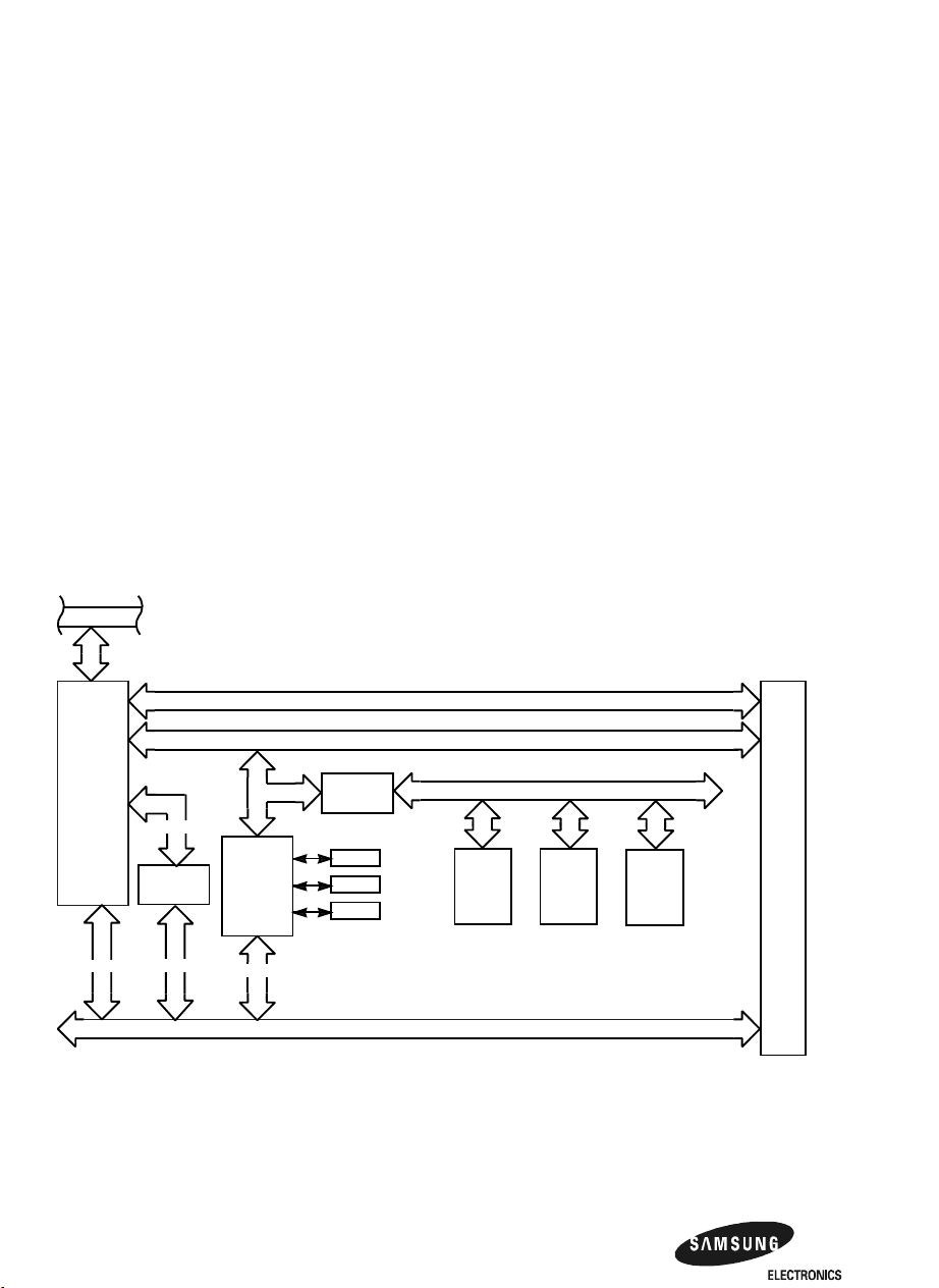
Figure 3–4 shows the AlphaPC 164UX ISA bus implementation with peripheral
devices and connectors. One dedicated ISA expansion slots are provided. System
support features such as serial lines, parallel port, and diskette controller are embedded on the module by means of an FDC37C666 combination controller chip.
Figure 3–4 AlphaPC 164UX ISA Bus Devices
PCI Bus
PCI-to-ISA
Bridge
82371SB
sd<7:0>
dd<11:0>
Combination
Controller
37C666
pc164ux.31
sa<15:0>
sa<19:0>
pc164ux.28
sa<7:0>
Transceivers
pc164ux.33
sa<19:8>
3–8 Functional Description
Transceivers
pc164ux.33
Diskette
Parallel
COM1/2
la<23:17>
sd<15:0>
J33
J13
J12
KBD
Controller
pc164ux.33
xd<7:0>
Real
Time
Clock
pc164ux.33
ISA0
NVRAM
pc164ux.28
pc164ux.29
J10
Page 46

3.3.1 Combination Controller
The AlphaPC 164UX uses the Standard Microsystems Corporation FDC37C666
Super I/O combination controller chip (see Figure 3–4). It is packaged in a 100-pin
QFP configuration. The chip provides the following ISA peripheral functions:
• Diskette controller–Software compatible to the Intel N82077 FDC. Integrates
the functions of the formatter/controller, digital data separator, write precompensation, and data-rate selection logic requiring no external filter components. Supports the 2.88MB drive format and other standard diskette drives
used with 5.25-inch and 3.5-inch media. FDC data and control lines are
brought out to a standard 34-pin connector (J33). A ribbon cable interfaces the
connector to one or two diskette drives.
• Serial ports–Two UARTs with full modem control, compatible with NS16450
or PC16550 devices, are brought out to two separate onboard, 9-pin
D-subminiature connectors (J12).
• Parallel port–The bidirectional parallel port is brought out to an onboard 25-pin
connector (J13). It can be brought out through a 25-pin female D-subminiature
connector on the bulkhead of a standard PC enclosure.
ISA Bus Devices
Functional Description 3–9
Page 47

Flash ROM Address Map
3.3.2 XD Bus Device
The AlphaPC 164UX XD bus drives a NVRAM,RTC,and KBDC devices.
3.3.3 ISA Expansion Slots
One ISA expansion slot is provided for plug-in ISA peripheral (J10).
3.3.4 ISA I/O Address Map
Table 3–1 lists the AlphaPC 164UX ISA I/O space address mapping.
Table 3–1 ISA I/O Address Map
Range (hex) Usage
060-060 i8042 PRT
064-064 i8042 PRT
1F0-1F7 ATAPI
2F8-2FE Serial port—COM2
378-37B Parallel Port—LPT2
3F0-3F5 Floppy
3F6-3F6 ATAPI
3F7-3F7 Floppy
3F8-3FE Serial port—COM1
3.4 Flash ROM Address Map
The flash ROM is mapped to three regions of memory. Access to the first two
regions is RO. The first two regions provide the software necessary to initialize the
system and transfer execution to the next level of software. When power is turned
on, address ranges 0 to 00.00FF.FFFF and 0F.FC00.0000 to 0F.FFFF.FFFF are
enabled. After the system has been initialized, these two address ranges are disabled.
Byte mode is then enabled in the 21164 and 21174. Byte mode is the only way to
access the flash ROM in address range 87.C000.0000 to 87.FFFF.FFFF. 21164 byte
instructions LDBU and STB must be used to access this region. Any other
instruction will produce UNDEFINED results with the possibility of damaging the
flash ROM.
3–10 Functional Description
Page 48

3.5 Interrupts
This section describes the AlphaPC 164UX interrupt logic. PCI-, ISA-, and 21174generated interrupts are described. Figure 3–5 shows the interrupt logic.
The PCI-to-ISA SIO bridge chip provides the functionality of two 8259 interrupt
control devices. These ISA-compatible interrupt controllers are cascaded so that 14
external and 2 internal interrupts are available. The PCI interrupt acknowledge command should be used to read the interrupt request vector from the SIO.
However, the AlphaPC 164UX system has more external interrupts than the SIO can
handle. They are sent to an external Shift Registers. This Shift Registers takes these
interrupts with parallel. When the Shift Registers are clocked,data is shifted toward
the serial output and generates irqchain2 finally. During reset, irq<3:0> convey the
system clocking ratios and delays, which are set by jumpers on J28.
Table 3–2 lists each system interrupt, its fixed interrupt priority level (IPL), and its
AlphaPC 164UX implementation. Table 3–3 lists each ISA bus interrupt and its
AlphaPC 164UX implementation.
Interrupts
Functional Description 3–11
Page 49
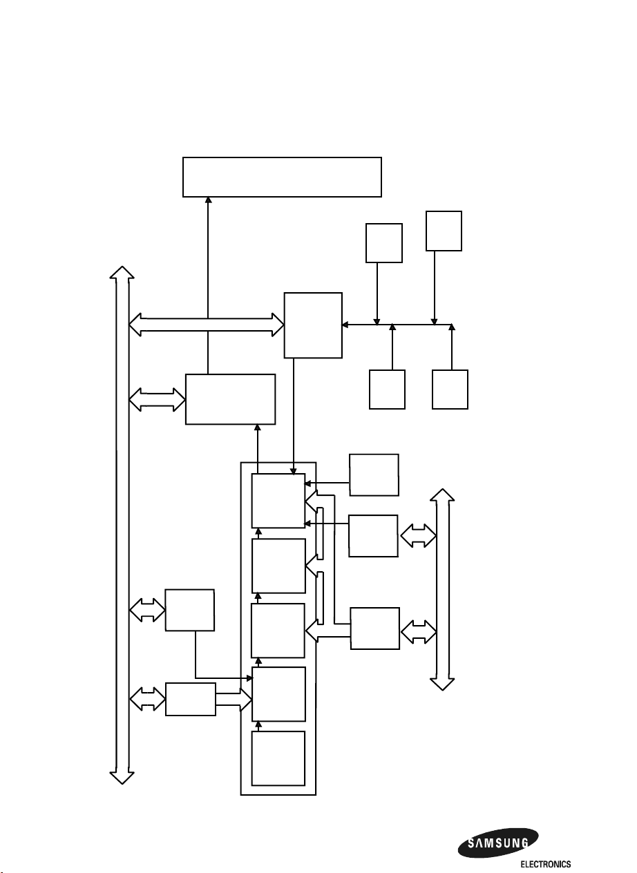
Interrupts
Figure 3–5 Interrupt Logic
Primary PCI Bus
21164
irq<0:3>
power_fail_irq
halt_irq
procirqs<6:0>
21174
mchk_irq
irqchain2
pc164ux.8-10
Shift
Register
Shift
Register
PCI to ISA
isairq
pc164ux.25
pc164ux.25
Bridge
(SIO)
*slotNirqX
pc164ux.2
FDC
irq<3,4,6,7>
irq<1,3:7,9:12,14,15>
pc164ux.28
Real
Time
flash_ready_irq
Flash
ROM
*scsiirq
SCSI
Controller
pc164ux.31
*irq8
Clock
pc164ux.33
pc164ux.8
pc164ux.24
ISA
Slot
pc164ux.29
irq<3:7,9:12,14,15>
irq<1,12>
pc164ux.33
KBD
Controller
3–12 Functional Description
Ethernet
Slot
64 PCI
Controller
pc164ux.26
*v3_slot0irq3
pc164ux.23
*v3_slot1irqX
Shift
Register
Shift
Register
Shift
Register
pc164ux.25
pc164ux.23
pc164ux.36
32 PCI
Slots
pc164ux.20-22
X can vary from a to d;
N can vary from 0 to 3.
*
Secondary PCI Bus
Page 50

Interrupts
Table 3–2 AlphaPC 164UX System Interrupts
21164 Interrupt IPL
irq<0> 20 Corrected system error Corrected ECC error and
irq<1> 21 — PCI and ISA interrupts
irq<2> 22 Interprocessor and
irq<3> 23 — Reserved
pwr_fail_irq 30 Powerfail interrupt Reserved
1
Suggested Usage AlphaPC 164UX Usage
sparse space reserved encodings detected by the 21174
timer interrupts
mchk_irq 31 System machine check
SIO NMI and 21174 errors
interrupt
hlt_irq — Halt Reserved
1
IPL = interrupt priority level (fixed).
Functional Description 3–13
Page 51

Interrupts
Table 3–3 ISA Interrupts
Interrupt
Number Interrupt Source
IRQ0 Internal timer
IRQ1 Keyboard
IRQ2 Interrupt from controller 2
IRQ3 COM2
IRQ4 COM1
IRQ5 Available
IRQ6 Diskette (floppy)
IRQ7 Parallel port
*IRQ8
IRQ9 Available
IRQ10 Available
IRQ11 Available
1
Reserved
IRQ12 Mouse
IRQ13 Available
IRQ14 IDE
IRQ15 IDE
1
The * symbol indicates an active low signal.
3–14 Functional Description
Page 52

3.6 System Clocks
Figure 3–6 shows the AlphaPC 164UX clock generation and distribution scheme.
The AlphaPC 164UX system includes input clocks to the microprocessor as well as
clock distribution for the various system memory and I/O devices. There are other
miscellaneous clocks for ISA bus support. System clocking can be divided into the
following three main areas:
• Microprocessor input clock — The input clock runs at the operating frequency
of the 21164 microprocessor. The AlphaPC 164UX supports cycle times from
3.33ns to 1.25 ns. This implies input clock frequencies from 300MHz to 800
MHz. The clock is provided by using a TQ2061. The TQ2061’s output is used as
the input clock for the 21164.
• Clock distribution — Clock distribution includes the distribution of system
clocks from the 21164 microprocessor to the system logic. The AlphaPC 164UX
clock distribution scheme is flexible enough to allow the majority of cycle-time
combinations to be supported. Because the PCI is synchronous to the system clock
generated by the 21164 microprocessor, the PCI cycle time is a multiple of the
21164 cycle time. This distribution scheme supports a PCI operation of 33 MHz.
System Clocks
• Miscellaneous clocks — The miscellaneous clocks include those needed for
ISA and the combination controller. These clocks are provided by a crystal and a
frequency generator with fixed scaling.
Functional Description 3–15
Page 53
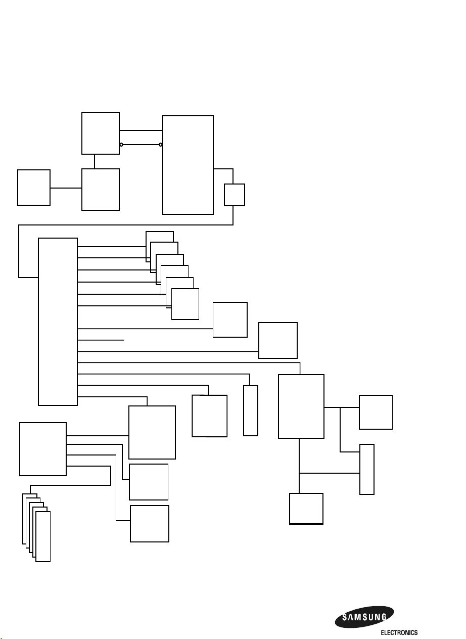
System Clocks
Figure 3–6 AlphaPC 164UX System Clocks
Oscillator
pc164ux.4
pc164ux.10
Clock Driver
(163344)
pc164ux.4
buf_dramclkax2
21174
buf_dramclkbx2
buf_dramclkcx2
buf_dramclkdx2
buf_dramclkex2
buf_dramclkfx2
p64_clk6
p64_clk5
p64_clk4
p64_clk3
p64_clk2
p64_clk1
p64_clk0
p32_clk7
p32_clk6
p32_clk5
p32_clk<4:0>
PCI
32 Slots
pc164ux.20-22
Clock Gen
(Fast)
TQ2061
pc164ux.4
Refclkout
Clock Gen
(Slow)
CY2907
pc164ux.4
Oscclkin
*Oscclkin
Sysclk
PCI to PCI
Bridge
(21052)
pc164ux.19
Arbiter
pc164ux.18
SCSI
Controller
pc164ux.24
Microprocessor
DIMM0
DIMM1
DIMM2
DIMM3
DIMM4
DIMM5
21164
pc164ux.2
Ethernet
Controller
pc164ux.26
CY2308
PLL
DMA
Hack
pc164ux.27
Arbiter
pc164ux.18
PCI
64 Slot
pc164ux.23
82371SB
Bridge
pc164ux.28
KBD
Controller
pc164ux.33
osc14mhz
v83_sysclk
14.3MHz
Oscillator
pc164ux.28
ISA
Slots
pc164lx.29
3–16 Functional Description
Page 54
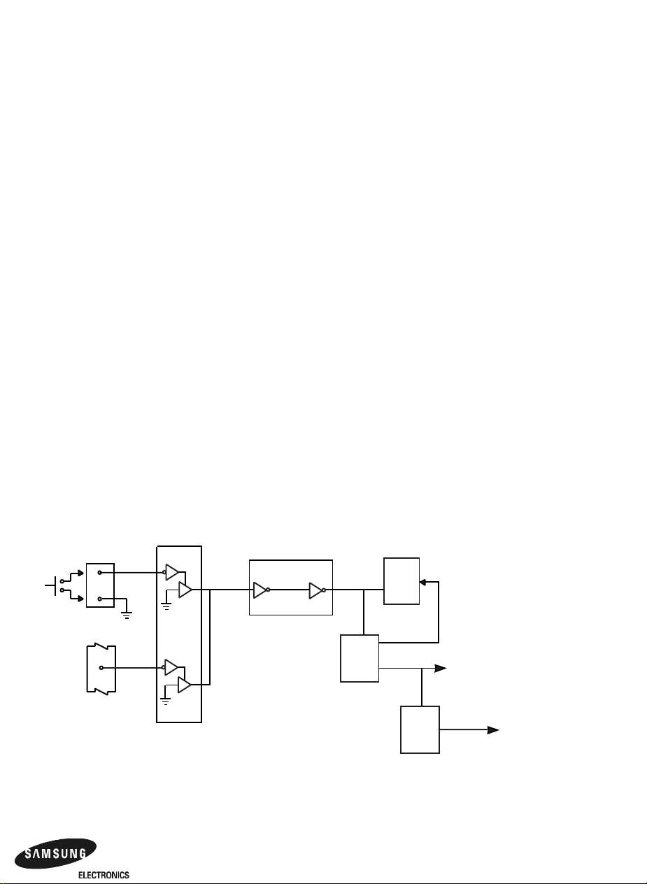
At system reset, the 21164 microprocessor’s procirq<3:0> pins are driven by the
clock divisor values set by four jumpers on J28. During normal operation, these signals are used for interrupt requests. The pins are either switched to ground or pulled
up in a specific combination to set the 21164 microprocessor’s internal divider.
The 21164 microprocessor produces the divided clock output signal sysclk that
drives the CY2308 PLL clock-driver chip. This clock provides the references to synchronize the 21164 microprocessor and the 21174 chip. The 21174 provides the system memory and I/O (PCI) clock references. It also provides system-level clocking
to DIMMs, PCI 64slot, the PCI-ISA bridge, the PCI-PCI controller,Ethernet Controller, DMA Hack and the PCI arbiter.
3.7 Reset and Initialization
An external reset switch can be connected to J37 (pc164UX.35). The reset function
initializes the 21164 microprocessor and the system logic. The vccok signal provides
a full system initialization, equivalent to a power-down and power-up cycle.
When dc_ok signal is inserted to 21174 chip, 21174 chip drives *p64_rst signal to
reset primary PCI devices and PCI to PCI bridge.
As soon as *p64_rst is inserted, PCI to PCI bridge drives *p32_rst signal to reset
secondary PCI devices
Reset and Initialization
Figure 3–7 System Reset and Initialization
Reset Switch
Power Supply
J37
pc164ux.35
2
1
J18
pc164ux.34
8
*rstswitch
vccok
HC125D
pc164ux.35
dc_oka
HCT14D
*dc_ok
pc164ux.35
dc_ok
21174
pc164ux.10
21164
pc164ux.2
*cpureset
*p64_rst
pci-pci
pc164ux.19
pci 64 slot
pci - isa bridge
ethernet controller
dma hack
*p32_rst
SCSI controller
pci 32 slots
Functional Description 3–17
Page 55

DC Power Distribution
3.8 DC Power Distribution
The AlphaPC 164UX drives its system power from a user-supplied PC power supply. The power supply must provide +12 V dc and -12 V dc, -5 V dc, +3 V dc, and
+5 V dc (Vdd). The dc power is supplied through power connector J18
(pc164ux.34), as shown in Figure 3–8. Power is distributed to the board logic
through dedicated power planes within the eight-layer board structure.
3–18 Functional Description
Page 56
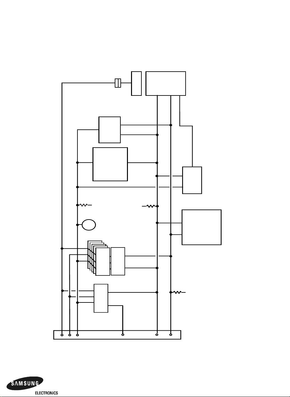
Figure 3–8 AlphaPC 164UX Power Distribution
Fan
21164
P/J35
pc164ux.26
Ethernet
controller
Integrated
Circuits/Clocks
(pci-isa,scsi,rtc,
srom,multi i/o,
data switch)
DC Power Distribution
pc164ux.1-2
+2.5V
pc164ux.34
Voltage
Regulator
Power
Connector
J18
+12 V
-12 V
10
+5 V (Vcc)
12
4,6,19,20
+5-V Pull-Ups
Spkr
pc164ux.20-22
PCI32 Conn.
pc164ux.23
ISA Conn.
Pull-Downs
pc164ux.23
PCI64 Conn.
-5 V
18
Gnd
3,5,7,13
15,16,17
Integrated
Circuits
(21174,dimm,
dimm buffer,
flash,sram,
arbiter)
+3.3-V Pull-Ups
+3.3 V
pc164ux.34
1,2,11
Functional Description 3–19
Page 57

Upgrading the AlphaPC 164UX
For higher system speed or greater throughput, you can upgrade SDRAM memory
by replacing DIMMs with those of greater size.
When configuring or upgrading SDRAM, observe the following rules:
• Each DIMM must be a 168-pin unbuffered version and have a frequency of
100 MHz.
• All DIMMs must be of equal size if they are in the same bank.
4.1 Upgrading SDRAM Memory
You can upgrade memory in the AlphaPC 164UX by adding more DIMMs or replacing the ones that you have with a greater size.
Use the following general guidelines:
1. Observe antistatic precautions. Handle DIMMs only at the edges to prevent
damage.
2. Remove power from the system.
4
3. Open levers and align the DIMM.
4. Firmly push the module into the connector. Ensure that the DIMM snaps into
the plastic locking levers on both ends.
5. Restore power to the system.
4.2 Increasing Microprocessor Speed
This section describes how to complete the following actions to increase microprocessor speed:
Upgrading the AlphaPC 164UX 4–1
Page 58

Increasing Microprocessor Speed
• Replace the Digital Semiconductor 21164 microprocessor with an Alpha chip
that has a higher speed rating.
• Reconfigure the clock divisor jumpers.
4.2.1 Preparatory Information
Caution: Static-Sensitive Component – Due to the sensitive nature of electronic
components to static electricity, anyone handling the microprocessor
must wear a properly grounded antistatic wriststrap. Use of antistatic
mats, ESD approved workstations, or exercising other good ESD practices is recommended.
A Samsung 21164 microprocessor with a higher speed rating is available from your
local distributor. See Appendix B for information about supporting products.
When replacing the microprocessor chip, also replace the thermal conducting
GRAFOIL pad. See Appendix B for information about the parts kit, which includes
the heat sink, GRAFOIL pad, two hex nuts, heat-sink clips, 60-mm fan, and four
screws.
4.2.2 Required Tools
The following tools are required when replacing the microprocessor chip:
A TS30 manual nut/torque driver (or equivalent) with the following attachments is
required to affix the heat sink and fan to the microprocessor’s IPGA package:
• 1/4-inch hex bit
• 7/16-inch socket with 1/4-inch hex drive
• #2 Phillips-head screwdriver bit
4.2.3 Removing the 21164 Microprocessor
Remove the microprocessor currently in place at location U55 by performing the following steps:
1. Unplug the fan power/sensor cable from connector J35 (see Figure 2–1).
2. Remove the four 6-32
the heat sink.
3. Remove the fan and fan guard.
4–2 Upgrading the AlphaPC 164UX
X 0.875-inch screws that secure the fan and fan guard to
Page 59

Increasing Microprocessor Speed
4. If the sink/chip/fan clip is used, remove it by unhooking its ends from around the
ZIF socket retainers.
5. Using a 7/16-inch socket, remove the two nuts securing the heat sink to the
microprocessor studs.
6. Remove the heat sink by gently lifting it off the microprocessor.
7. Remove and discard the GRAFOIL heat conduction pad.
8. Thoroughly clean the bottom surface of the heat sink before affixing it to the
new microprocessor.
9. Lift the ZIF socket actuator handle to a full 90° angle.
10. Remove the microprocessor chip by lifting it straight out of the socket.
4.2.4 Installing the 21164 Microprocessor
Install the new microprocessor in location U55 by performing the following steps:
Note: Install the heat sink only after the microprocessor has been assembled to
the ZIF socket.
1. Observe antistatic precautions.
2. Lift the ZIF socket actuator handle to a full 90° angle.
3. Ensure that all the pins on the microprocessor package are straight.
4. The ZIF socket and microprocessor are keyed to allow for proper installation.
Align the microprocessor, with its missing AD01 pin, with the corresponding
plugged AD01 position on the ZIF socket. Gently lower into position.
5. Close the ZIF socket actuator handle to its locked position.
6. Install the heat sink and heat-sink fan as directed in the following steps. A heatsink/fan kit is available from the vendor listed in Appendix B. Refer to Figure 4–1
for heat-sink and fan assembly details.
Upgrading the AlphaPC 164UX 4–3
Page 60
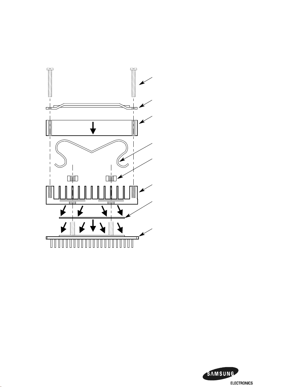
Increasing Microprocessor Speed
Figure 4–1 Fan/Heat-Sink Assembly
Airflow
Screw, 6-32 x 0.875 in
Qty 4
Guard, Fan
Fan
Clip, Heat Sink/Chip/Fan
Nut, Hex, 1/4-20, 2011-T3
Aluminum, 0.438 in Across
Flats, Qty 2
Torque to 20 +/- 2 in-lbs
Heat Sink, with Fan
Mounting Holes
Thermal Pad
a. Put the GRAFOIL thermal pad in place. The GRAFOIL pad is used to improve
the thermal conductivity between the chip package and the heat sink by replacing micro air pockets with a less insulative material. Perform the following
steps to position the GRAFOIL pad:
1. Perform a visual inspection of the package slug to ensure that it is free of
contamination.
2. Wearing clean gloves, pick up the GRAFOIL pad. Do not perform this
with bare hands because skin oils can be transferred to the pad.
3. Place the GRAFOIL pad on the gold-plated slug surface and align it
with the threaded studs.
4–4 Upgrading the AlphaPC 164UX
Alpha 21164
FM-06013.AI4
Page 61

Increasing Microprocessor Speed
b. Attach the microprocessor heat sink. The heat-sink material is clear anodized,
hot-water-sealed, 6061-T6 aluminum. The nut material is 2011-T3 aluminum
(this grade is critical). Perform the following steps to attach the heat sink:
1. Observe antistatic precautions.
2. Align the heat-sink holes with the threaded studs on the ceramic package.
3. Handle the heat sink by the edges and lower it onto the chip package,
taking care not to damage the stud threads.
4. Set a calibrated torque driver to 20 in-lbs, ±2 in-lbs (2.3 Nm, ±0.2 Nm).
The torque driver should have a mounted 7/16-inch socket.
5. Insert a nut into the 7/16-inch socket, place on one of the studs, and
tighten to the specified torque. Repeat for the second nut.
6. If the sink/chip/fan clip is used, properly install it by positioning it over
the assembly and hooking its ends around the ZIF socket retainers.
c. Attach the heat-sink fan assembly:
1. Place the fan assembly on top of the heat sink, aligning the fan mounting
holes with the corresponding threaded heat-sink holes. Align the fan so
that the fan power/sensor wires exit the fan closest to connector J35 (see
Figure 2–1). Fan airflow must be directed into the heat sink (fan label
facing down toward the heat sink).
2. Place the fan guard on top of the fan. Orient the guard so that the corner
mounting areas lay flush against the heat sink.
3. Secure the fan and fan guard to the heat sink with four 6-32
X 0.875-inch
screws.
4. Plug the fan power/sensor cable into connector J35.
Important: When installing the microprocessor, you must change the frequency of
its clock output by setting the system clock divisor jumpers, as described
in Section 2.2.
Upgrading the AlphaPC 164UX 4–5
Page 62

Power and Environmental Requirements
5.1 Power Requirements
The AlphaPC 164UX motherboard requires a minimum of a 300 watt power supply.
The power supply must be ATX-compliant.
Table 5–1 Power Supply DC Current Requirements
Voltage Current
+3.3 Vdc,±5% 14 A
+5 Vdc,
-5 Vdc,±5% 0.5 A
+12 Vdc,
-12 Vdc,
Caution: Fan sensor required. The 21164 microprocessor cooling fan must
±5% 25 A
±5% 10 A
±5% 0.5 A
have a built-in sensor that will drive a signal if the airflow stops. The
sensor is connected to the motherboard connector J35. When the signal
is generated, the speaker generates a tone..
5
5.2 Environmental Requirements
The 21164 microprocessor is cooled by a small fan blowing directly into the chip’s
heat sink. The AlphaPC 164UX motherboard is designed to run efficiently using
only this fan. Additional fans may be necessary depending upon cabinetry and the
requirements of add-in cards and disk drives.
Power and Environmental Requirements 5–1
Page 63

Physical Parameters
The AlphaPC 164UX motherboard is specified to run within the environment listed
in Table 5–2.
Table 5–2 AlphaPC 164UX Motherboard Environmental Requirements
Parameter Specification
Operating Temperature 10°C to 40°C (50°F to 104°F)
Storage Temperature -55°C to 125°C ( -67°F to 257°F)
Relative Humidity 10% to 90% with maximum wet bulb temperature 28°C
Rate of (dry bulb) temperature
change
5.3 Physical Parameters
This section has four parts: the first illustrates the board dimensions for AlphaPC
164UX. the second shows the distances between the board mounting holes and the
edges of the board; the third shows the vertical clearances required by the board
components at all points within the border of the AlphaPC 164UX.
All holes and board measurements are compliant with the ATX 2.01 specification.
The AlphaPC 164UX exceeds the ATX height indications in two places. The first is
(the 2.5’ region).The second is at the location of the SCSI connectors(the 1.0’ region
to the left of the second PCI slots).
(82°F) and a minimum dew point 2°C (36°F)
11°C/hour
±2°C/hour (20°F/hour ±4°F/hour)
the fourth shows the ATX I/O shield dimensions.
5.3.1 Board Dimensions
The AlphaPC 164UX motherboard is an ATX-size printed wiring board (PWB) with
the following dimensions:
• Length: 30.48 cm (12.0 in ±0.0005 in)
• Width: 24.38 cm (9.6 in ±0.0005 in)
• Height: 6.86 cm (2.7 in)
The board can be used in certain desktop and deskside systems that have adequate
clearance for the 21164 heat sink and its cooling fan. All ISA and PCI expansion
slots are usable in standard desktop or deskside enclosures.
5–2 Power and Environmental Requirements
Page 64
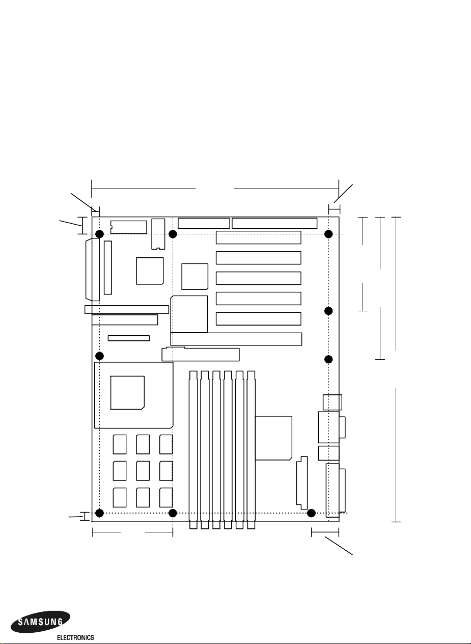
5.3.2 Board Measurements and Hole Locations
Figure 5–1 shows the Board Measurements and Hole Locations for the AlphaPC
164UX.
Figure 5–1 Board measurement and Hole Position Diagram
Physical Parameters
.250"
.650"
9.600"
.400"
3.750"
5.550"
12.00"
.250"
3.1"
Board Measurements and Hole Locations
Power and Environmental Requirements 5–3
1.300"
Page 65
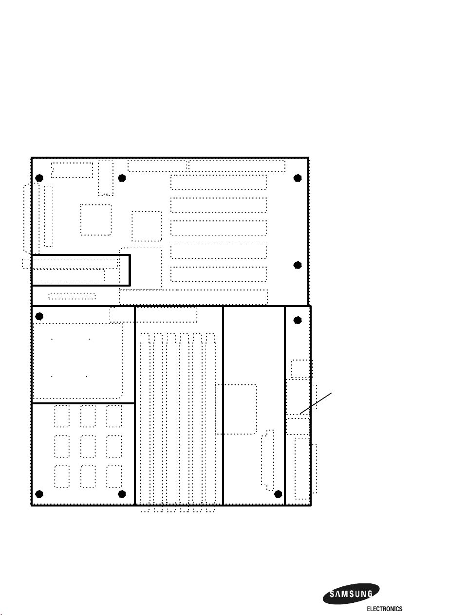
Physical Parameters
5.3.3 Board Vertical Clearance
Figure 5–2 shows the Board Vertical Clearance for the AlphaPC 164UX.
Figure 5–2 Board Vertical Clearance Diagram
0.5"
1.0"
2.5"
1.5"
0.5"
Vertical Clearance Requirements
5–4 Power and Environmental Requirements
1.5"
1.0"
Page 66
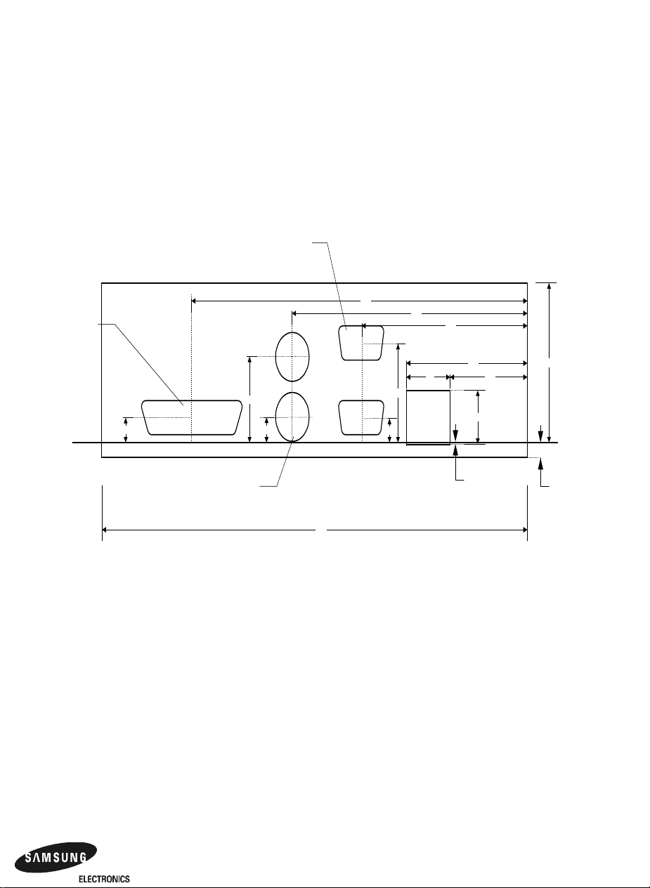
5.3.4 ATX I/O Shield Requirements
Figure 5–3 shows the ATX I/O shield dimensions for the AlphaPC 164UX.
Figure 5–3 ATX I/O Shield Dimensions
Standard 9 pin DSUB
connector cutouts
with these center
Physical Parameters
points
Standard 25 pin
DSUB connector
cutout with this center
point
4.924
.856
.247
Radius = .490 on both
circles. Dimensions
represent center of
.256
circles.
6.250
3.454
2.436
1.774
.640
.990
.240
1.134
0.54
.020
1.60
.150
Power and Environmental Requirements 5–5
Page 67

This appendix describes the mapping of 21164 40-bit physical addresses to memory
and I/O space addresses. It also describes the translation of a 21164-initiated address
(addr_h<39:4>) into a PCI address (ad<63:0>) and the translation of a PCI-initiated
address into a physical memory address.
PCI addressing topics include dense and sparse address space and scatter-gather
address translation for DMA operations.
1.1 Address Map
The system address mapping operates with byte/word transactions enabled or disabled. Byte/word operation is controlled by PYXIS_CTRL1<0> (IOA_BEN).
Table A–1 shows system address mapping operations when IOA_BEN equals 0
(byte/word operation disabled).
A
System Address Space
Table A–1 Physical Address Map (Byte/Word Mode Disabled)
21164 Address
00.000.0000 – 01.FFFF.FFFF
E.0000.0000 – E.FFFF.FFFF
80.0000.0000 – 83.FFFF.FFFF
84.0000.0000 – 84.FFFF.FFFF
85.0000.0000 – 85.7FFF.FFFF
85.8000.0000 – 85.BFFF.FFFF
85.C000.0000 – 85.FFFF.FFFF
86.0000.0000 – 86.FFFF.FFFF
87.0000.0000 – 87.1FFF.FFFF
1
Size (GB) Selection
8.00 Main memory
4.00 Dummy memory region
16.00 PCI sparse memory region 0, 512MB
4.00 PCI sparse memory region 1, 128MB
2.00 PCI sparse memory region 2, 64MB
1.00 PCI sparse I/O space region A, 32MB
1.00 PCI sparse I/O space region B, 32MB
4.00 PCI dense memory
0.50 PCI sparse configuration space
System Address Space A–1
(Sheet 1 of 2)
Page 68

Address Map
Table A–1 Physical Address Map (Byte/Word Mode Disabled)
21164 Address
87.2000.0000 – 87.3FFF.FFFF
87.4000.0000 – 87.4FFF.FFFF
87.5000.0000 – 87.5FFF.FFFF
87.6000.0000 – 87.6FFF.FFFF
87.7000.0000 – 87.7FFF.FFFF
87.8000.0000 – 87.8FFF.FFFF
87.9000.0000 – 87.9FFF.FFFF
87.A000.0000 – 87.AFFF.FFFF
87.B000.0000 – 87.FFFF.FFFF
1
All addresses in the range of 80.0000.0000 and 8F.FFFF.FFFF are aliased. Address bits 36 through
38 are ignored in the address.
1
Size (GB) Selection
0.50 PCI special/interrupt acknowledge
0.25 21174 main CSRs
0.25 21174 memory control CSRs
0.25 21174 PCI address translation
0.25 Reserved
0.25 21174 miscellaneous CSRs
0.25 21174 power management CSRs
0.25 21174 interrupt control CSRs
1.25 Reserved
(Sheet 2 of 2)
Table A–2 shows system address mapping operations when IOA_BEN equals 1
(byte/word operation enabled).
Table A–2 Physical Address Map (Byte/Word Mode Enabled)
21164 Address Size (GB) Selection
(Sheet 1 of 2)
00.000.0000 – 01.FFFF.FFFF
E.0000.0000 – E.FFFF.FFFF
80.0000.0000 – 83.FFFF.FFFF
84.0000.0000 – 84.FFFF.FFFF
85.0000.0000 – 85.7FFF.FFFF
85.8000.0000 – 85.BFFF.FFFF
85.C000.0000 – 85.FFFF.FFFF
86.0000.0000 – 86.FFFF.FFFF
87.0000.0000 – 87.1FFF.FFFF
87.2000.0000 – 87.3FFF.FFFF
87.4000.0000 – 87.4FFF.FFFF
87.5000.0000 – 87.5FFF.FFFF
A–2 System Address Space
8.00 Main memory
4.00 Dummy memory region
16.00 PCI sparse memory region 0, 512MB
4.00 PCI sparse memory region 1, 128MB
2.00 PCI sparse memory region 2, 64MB
1.00 PCI sparse I/O space region A, 32MB
1.00 PCI sparse I/O space region B, 32MB
4.00 PCI dense memory
0.50 PCI sparse configuration space
0.50 PCI special/interrupt acknowledge
0.25 21174 main CSRs
0.25 21174 memory control CSRs
Page 69

Address Map
Table A–2 Physical Address Map (Byte/Word Mode Enabled)
21164 Address Size (GB) Selection
87.6000.0000 – 87.6FFF.FFFF
87.7000.0000 – 87.7FFF.FFFF
87.8000.0000 – 87.8FFF.FFFF
87.9000.0000 – 87.9FFF.FFFF
87.A000.0000 – 87.AFFF.FFFF
87.B000.0000 – 87.BFFF.FFFF
88.0000.0000 – 88.FFFF.FFFF
98.0000.0000 – 98.FFFF.FFFF
A8.0000.0000 – A8.FFFF.FFFF
B8.0000.0000 – B8.FFFF.FFFF
89.0000.0000 – 89.FFFF.FFFF
99.0000.0000 – 99.FFFF.FFFF
A9.0000.0000 – A9.FFFF.FFFF
B9.0000.0000 – B9.FFFF.FFFF
8A.0000.0000 – 8A.FFFF.FFFF
9A.0000.0000 – 9A.FFFF.FFFF
AA.0000.0000 – AA.FFFF.FFFF
BA.0000.0000 – BA.FFFF.FFFF
8B.0000.0000 – 8B.FFFF.FFFF
9B.0000.0000 – 9B.FFFF.FFFF
AB.0000.0000 – AB.FFFF.FFFF
BB.0000.0000 – BB.FFFF.FFFF
C7.C000.0000 – C7.FFFF.FFFF
1
Address bits 37 and 38 are generated by the 21164 and not by software. These address bits are
used by the 21164 to indicate to external hardware that this transaction is a byte, word, longword,
or quadword operation.
2
Read/write transactions to flash ROM must be done with byte transactions to address range
87.C000.0000 through 87.FFFF.FFFF. All other transaction types will produce UNDEFINED
results.
0.25 21174 PCI address translation
0.25 Reserved
0.25 21174 miscellaneous CSRs
0.25 21174 power management CSRs
0.25 21174 interrupt control CSRs
0.25 Reserved
4.00 PCI memory space INT8
1
4.00 PCI memory space INT4
1
4.00 PCI memory space INT2
1
4.00 PCI memory space INT1
4.00 PCI I/O space INT8
1
4.00 PCI I/O space INT4
1
4.00 PCI I/O space INT2
1
4.00 PCI I/O space INT1
4.00 PCI configuration space, type 0, INT8
1
4.00 PCI configuration space, type 0, INT4
1
4.00 PCI configuration space, type 0, INT2
1
4.00 PCI configuration space, type 0, INT1
4.00 PCI configuration space, type 1, INT8
1
4.00 PCI configuration space, type 1, INT4
1
4.00 PCI configuration space, type 1, INT2
1
4.00 PCI configuration space, type 1, INT1
2
1.00 Flash ROM read/write space
(Sheet 2 of 2)
System Address Space A–3
Page 70

Address Map
The 21164 address space is divided into two regions using physical address <39>:
• 0 – 21164 access is to the cached memory space.
• 1 – 21164 access is to noncached space. This noncached space is used to access
memory-mapped I/O devices. Mailboxes are not supported.
The noncached space contains the CSRs, noncached memory space (for diagnostics),
and the PCI address space. The PCI defines three physical address spaces: a 64-bit
PCI memory space, a 4GB PCI I/O space, and a 256 byte-per-device PCI configuration space. In addition to these three address spaces on the PCI, the 21164’s noncached space is also used to generate PCI interrupt acknowledge and special cycles.
The 21164 has visibility to the complete address space. It can access the cached
memory region, the CSR region, the PCI memory region, the PCI I/O region, and
the configuration regions (see Figure 1–1).
The PCI devices have a restricted view of the address space. They can access any
PCI device through the PCI memory space or the PCI I/O space; but they have no
access to the PCI configuration space. The system restricts access to the system
memory (for DMA operations) to the use of five programmable windows in the PCI
memory space (see Figure 1–1).
A–4 System Address Space
Page 71
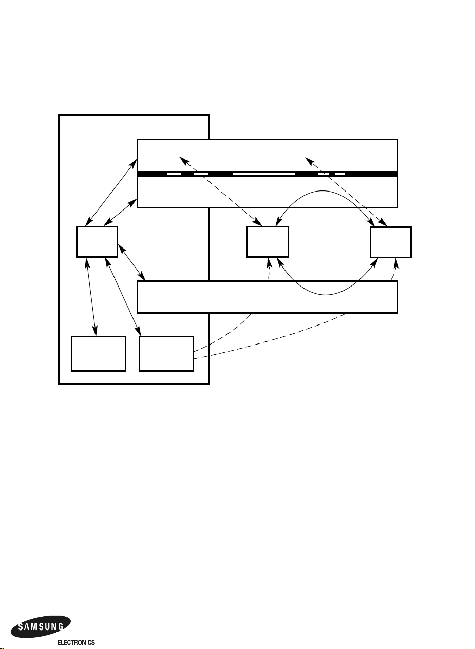
Figure 1–1 Address Space Overview
21164
Environment
Main System
Memory
Address Map
PCI Window
PCI
Device
PCI
Device
LJ-05395.AI4
21164
CSRs
PCI
Memory Space
PCI I/O Space
PCI
Configuration
Space
DMA access to the system memory is achieved using windows in one of the following three ways:
• Directly, using the “Monster Window” with dual-address cycles (DAC), where
ad<33:0> equals addr_h<33:0>.
• Directly-mapped, by concatenating an offset to a portion of the PCI address.
• Virtually, through a scatter-gather translation map. The scatter-gather map
allows any 8KB page of PCI memory address region to be redirected to any
8KB cached memory page, as shown in Figure 1–2.
System Address Space A–5
Page 72
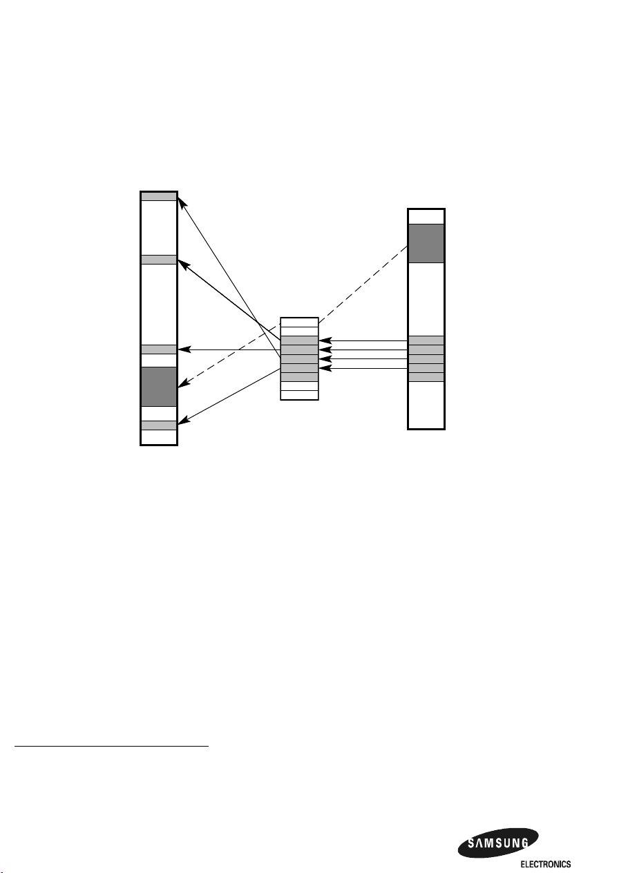
PCI Address Space
Figure 1–2 Memory Remapping
21164 CPU
Cached Memory Space (8GB)
8KB
Page
PCI Memory
Space
PCI Window
Direct Map
PCI Window
Scatter-Gather
Map
LJ-05396.AI4
1.2 PCI Address Space
The system generates 32-bit PCI addresses but accepts both 64-bit address (DAC1)
cycles and 32-bit PCI address (SAC2) cycles. Accessing main memory is as follows:
• Window 4, the “Monster Window,” provides full access to main memory. It is
accessed by DAC only with ad<40> equal to 1. Memory address addr_h<33:0>
equals PCI address ad<33:0>.
• Window 3 can be either DAC or SAC, but not both. If DAC, ad<63:40> must be
zero, ad<39:32> must match the DAC register, and ad<31:0> must hit in window 3.
• Windows 0, 1, and 2 are SAC-only.
1 Dual-address cycle (PCI 64-bit address transfer) requires that address bits <63:32> con-
tain a nonzero value.
2 Single-address cycle (PCI 32-bit address transfer) requires that address bits <63:32> con-
tain a value of zero.
A–6 System Address Space
Page 73

1.3 21164 Address Space
Figure 1–3 shows an overview of the 21164 address space. Figure 1–4 shows how
the 21164 address map translates to the PCI address space and how PCI devices
access the 21164 memory space using DMA transactions. The PCI memory space is
double mapped via dense and sparse space.
The 21164 I/O address map has the following characteristics:
• Provides 4GB of dense
ory space.
• Provides abundant PCI sparse
regions have byte granularity and is the safest memory space to use (that is, no
prefetching). Furthermore, the larger the space the less likely software will need
to dynamically relocate the sparse-space segments. The main problem with
sparse space is that it wastes 21164 address space (for example, 16GB of 21164
address space maps to 512MB of PCI sparse space).
The system provides three PCI sparse-space memory regions, allowing 704MB
of total sparse-space memory. The three regions are relocatable using the
HAE_MEM CSR. The simplest configuration allows for 704MB of contiguous
memory space.
21164 Address Space
1
address space to completely map the 32-bit PCI mem-
1
memory address space because sparse-space
– 512MB region, which may be located in any naturally aligned 512MB seg-
ment of the PCI memory space. Software programmers may find this region
sufficient for their needs and can ignore the remaining two regions.
– 128MB regions, which may be located on any naturally aligned 128MB seg-
ment of the PCI memory space.
– 64MB region, which may be located on any naturally aligned 64MB seg-
ment of the PCI memory space.
• Limits the PCI I/O space to sparse space. Although the PCI I/O space can handle
4GB, most PCI devices will not exceed 64KB for the foreseeable future. The
system provides 64MB of sparse I/O space because address decoding is faster.
• Provides two PCI I/O sparse-space regions: region A, which is 32MB and is
fixed in PCI segment 0–32MB; and region B, which is also 32MB, but is relocatable using the HAE_IO register.
1 Dense and sparse space address space are described later in this chapter.
System Address Space A–7
Page 74
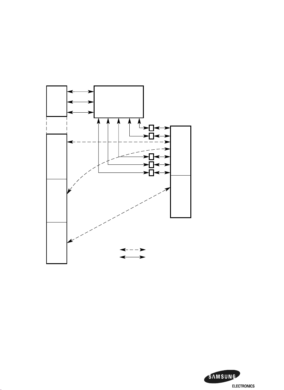
21164 Address Space
Figure 1–3 21164 Address Space Configuration
21164
Memory Space
Cached
Memory
Reserved
PCI Memory
Dense Space
PCI Memory
Sparse Space
PCI I/O
Space
Scatter-Gather
or
Direct
Translation
PCI Windows
PCI Memory
Space
PCI I/O
Space
21164 Programmed I/O
DMA Read/Write
LJ-05397.AI4
A–8 System Address Space
Page 75
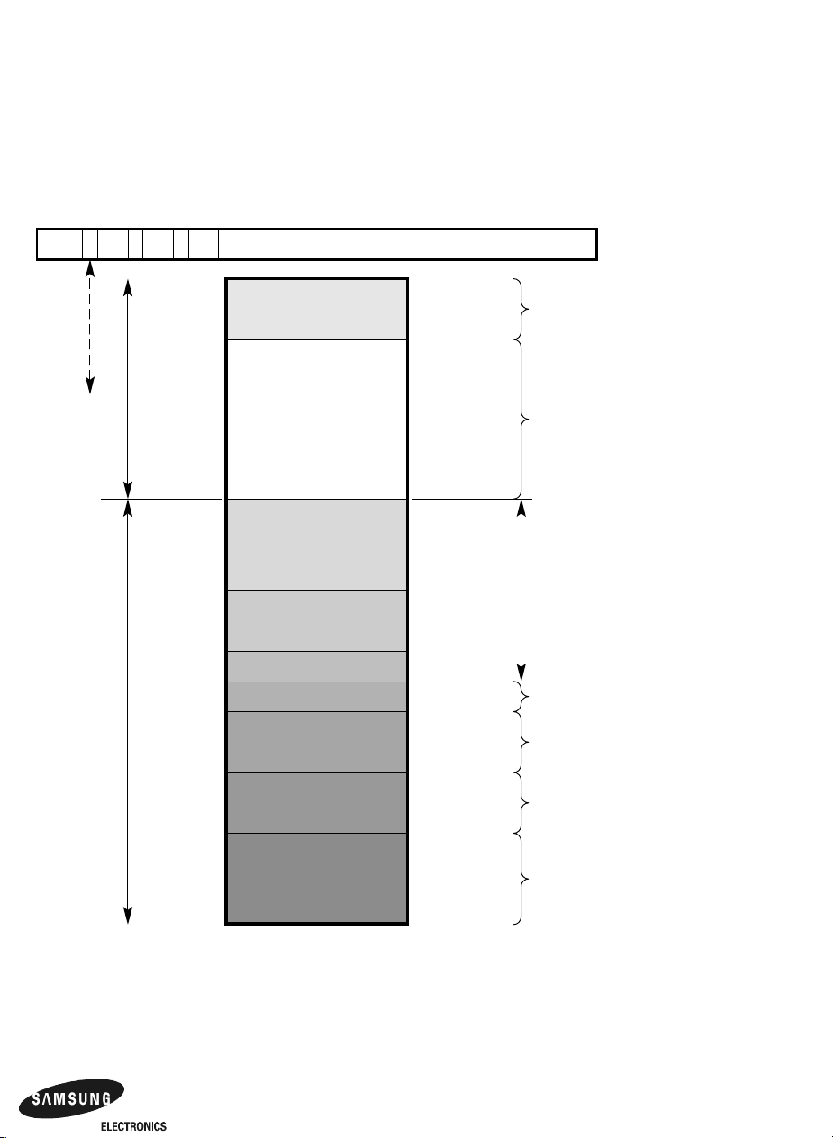
Figure 1–4 21164 and DMA Read and Write Transactions
21164 Address Space
0=Cached
Memory
Space
1=Noncached
I/O
Space
313233343536373839 30
0Size
000XX
00XXX 80.0000.0000
0100X 84.0000.0000
01010 85.0000.0000
01011 85.8000.0000
0110X 86.0000.0000
0111X 87.0000.0000
1000X 88.0000.0000
00.0000.0000
01.FFFF.FFFF
02.0000.0000
7F.FFFF.FFFF
83.FFFF.FFFF
84.FFFF.FFFF
86.FFFF.FFFF
87.FFFF.FFFF
8B.FFFF.FFFF
00
Physical
Address
8GB Cached
Memory
Reserved
PCI Memory
Sparse Space
704MB Maximum
PCI I/O Sparse
Space — 64MB
PCI Memory Dense
Space — 4GB
PCI Configuration,
CIA CSRs, Flash ROM
Byte/Word PCI
Space — 16GB
LJ-04868.AI4
System Address Space A–9
Page 76

21164 Address Space
A.3.1 System Address Map
Figure 1–5 shows the following system address regions:
• Main memory address space contains 8GB. All transactions contain 64 bytes, are
cache-block aligned, and are placed in cache by the 21164. Both Istream and
Dstream transactions access this address space.
• PCI sparse-space memory region 1 contains 512MB. Noncached 21164 read/write
transactions are allowed, including byte, word, tribyte, longword (LW), and quadword (QW) types. There is no read prefetching.
• PCI sparse-space memory region 2 contains 128MB.
• PCI sparse-space memory region 3 contains 64MB.
• PCI I/O sparse-space memory region A contains 32MB and is not relocatable.
• PCI I/O sparse-space memory region B contains 32MB and is relocatable by
way of the HAE_IO register.
• PCI dense memory space contains 4GB for 21164 noncached 21164 transac-
tions. It is used for devices with access granularity greater or equal to a LW.
Read prefetching is allowed, and thus read transactions can have no side effects.
• The PCI configuration space is used for noncached 21164 access. Sparse-space
read/write transactions are allowed, including byte, word, tribyte, LW, and QW
types. Prefetching of read data is not allowed.
Figure 1–6 shows a detailed view of PCI configuration space that includes 21174
CSRs. The 21174 CSR address space is chosen for hardware convenience.
A–10 System Address Space
Page 77
Figure 1–5 System Address Map
21164 Address Space
Main Memory — 8GB
34 333839 3435
00000
0
Memory Address
PCI Sparse Memory Space — 512MB Region 1
35
000
X
1
0
PCI Memory Address <28:2>
PCI Sparse Memory Space — 128MB Region 2
35
0
0
000
X
1
1
31 21034 33 323839
PCI Memory Address <26:2>
PCI Sparse Memory Space — 64MB Region 3
1
0
X
35
00
31 21034 33 323839
30
1
10
PCI Memory Address <25:2>
PCI I/O Sparse Space — 32MB Region A
31 21034 33 323839
30
29
1
03500
X
1
10
1
PCI I/O Address <24:2>
Size
Size
Size
Size
0
034 333839
2367
000
367
00
0
367
0
000
367
0
000
PCI I/O Sparse Space — 32MB Region B
31 21034 33 323839
30129
1
03500
X
1
11
PCI I/O Address <24:2>
PCI Memory Dense Space — 4GB
35
0
1
00
X
31 21034 33 323839
30029
1
PCI Memory Address <31:2>
PCI Configuration Space
31 21034 33 323839
28 27
03500
111
X
1
CSR
Space
Address
System Address Space A–11
367
Size
367
Size
LJ-05398.AI4
0
000
0
01
0
00
Page 78
21164 Byte/Word PCI Space
Figure 1–6 21174 CSR Space
PCI Configuration Space
28 27
31 21034 33 323839
Size (GB)
0.5
0.5
0.25
0.25
0.25
0.25
2.00
CSR
Space
Contents
PCI Configuration Space
PCI IACK/Special Cycle
21174 Main CSRs
Main Memory Control CSRs
21174 Address Translation
Reserved
Miscellaneous
03500
X
111
CPU Address
31 30 29 28
000
001
0100
0101
0110
0111
1
1
1.4 21164 Byte/Word PCI Space
The 21164 supports byte/word instructions that allow software to perform byte granularity transactions to and from I/O space without using sparse address space. This
space is divided into four regions: memory, I/O, configuration – type 0, and configuration – type 1, as shown in Figure 1–7.
Address
367
00
Size
FM-06062.AI4
0
A–12 System Address Space
Page 79
Figure 1–7 Byte/Word PCI Space
PCI Memory Space — 4GB
3637 35 34 33 323839
Size 00
1
31 210
01X00
PCI Memory Address <31:2>
PCI I/O Space — 4GB
31 03637 35 34 33 323839
Size
1
11X00
PCI Type 0 Configuration Space — 4GB
31 2103637 35 34 33 323839
Size 00
1
01X10
PCI Configuration Address <31:2>
PCI Type 1 Configuration Space — 4GB
31 2103637 35 34 33 323839
Size 01
1
11X10
PCI Configuration Address <31:2>
21164 Byte/Word PCI Space
PCI I/O Address
LJ-05399.AI4
Operations are the same for the four regions. The 21164 will issue a single byte/word
read or write transaction for PCI byte and word instructions. The 21164 will not
pack longword load instructions. The 21164 can pack up to eight longword store
instructions for a single 32-byte block into one transaction. Up to four quadword
instructions can also be packed to the same 32-byte block. Byte/word support is
enabled when 21164 IPR register ICSR<17> equals 1 and when 21174 CSR register
PYXIS_CTRL1<0> also equals 1.
System Address Space A–13
Page 80

21164 Byte/Word PCI Space
Table 1–3 shows noncached 21164 addresses when byte/word support is enabled.
Table A–3 21164 Byte/Word Addressing
addr_h
Instruction
LDQ 00 INT8 —— —
LDL 01 addr_h<3:2> —Undefined—
LDWU 10 addr_h<3:1> —— Undefined
LDBU 11 addr_h<3:0> —— —
STQ 00 INT4 Mask — — —
STL 01 INT4 Mask — — —
STW 10 addr_h<3:1> —— Undefined
STB 11 addr_h<3:0> —— —
<38:37>
A.4.1 21164 Size Field
Table A–4 shows the calculation of the 21164 size field.
Table A–4 21164 Byte/Word Translation Values
Size<38:37> Data Size
00 INT8 (Quadword — 8 bytes, 64 bits)
01 INT4 (Longword — 4 bytes, 32 bits)
int4_valid
<3> <2> <1> <0>
10 INT2 (Word — 2 bytes, 16 bits)
11 INT1 (Byte — 1 byte, 8 bits)
The following transactions use single data transfers on the PCI:
• INT1 and INT2 read and write transactions
• INT4 read transactions
The following transactions have multiple data transfers on the PCI:
• INT4 write transactions
• INT8 read and write transactions
A–14 System Address Space
Page 81

1.5 Cacheable Memory Space
Cacheable memory space is located in the range 00.0000.0000 to 01.FFFF.FFFF. The
21174 recognizes the first 8GB to be in cacheable memory space. The block size is
fixed at 64 bytes. Read and flush commands to the 21164 caches occur for DMA
traffic.
1.6 PCI Dense Memory Space
PCI dense memory address space is located in the range 86.0000.0000 to
86.FFFF.FFFF. This address space is typically used for memory-like data buffers
such as a video frame buffer or a nonvolatile RAM (NVRAM). Dense space does not
allow byte or word access, but has the following advantages over sparse space:
• Contiguous locations — Some software, such as the default graphics routines of
the Windows NT operating system, requires memory-like transactions. These
routines cannot use sparse-space addresses, because they require transactions on
the PCI bus to be at adjacent 21164 addresses, instead of being widely separated
as in sparse space. As a result, if the user-mode driver manipulates its frame
buffer in sparse space, it cannot hand over the buffer to the common
Windows NT operating system graphics code.
Cacheable Memory Space
• Higher bus bandwidth — PCI bus burst transfers are not usable in sparse space
except for a 2-longword burst for quadword write transactions. Dense space is
defined to allow both burst read and write transactions.
• Efficient read/write buffering — In sparse space, separate transactions use sepa-
rate read or write buffer entries. Dense space allows separate transactions to be
collapsed in read and write buffers (as the 21164 does).
• Few memory barriers (MBs) — In general, sparse-space transactions are sepa-
rated by MB instructions to avoid read/write buffer collapsing. Dense-space
transactions only require barriers when explicit ordering is required by the software.
Dense space is provided for the 21164 to access PCI memory space, not for access to
PCI I/O space. Dense space has the following characteristics:
• It holds a one-to-one mapping between 21164 addresses and PCI addresses.
A longword address from the 21164 will map to a longword on the PCI with no
shifting of the address field. Hence, the term dense space. Sparse space, on the
other hand, maps a large piece of 21164 memory space (32 bytes) to a small
piece (such as a byte) on the PCI.
System Address Space A–15
Page 82

PCI Dense Memory Space
• The concept of dense space (and sparse space) is applicable only to a 21164-gen-
erated address. There is no such thing as dense space (or sparse space) for a PCI
generated address.
• Byte or word transactions are not possible in dense space. The minimum access
granularity is a longword on write transactions and a quadword on read transactions. The maximum transfer length is 32 bytes (performed as a burst of eight
longwords on the PCI). Any combination of longwords may be valid on write
transactions. Valid longwords surrounding an invalid longword(s) (called a hole)
are required to be handled correctly by all PCI devices. The 21174 will allow
such holes to be issued.
• Read transactions will always be performed as a burst of two or more longwords
on the PCI because the minimum granularity is a quadword. The 21164 can
request a longword but the 21174 will always fetch a quadword, thus prefetching
a second longword. Therefore, this space cannot be used for devices that have
read side effects. Although a longword may be prefetched, the prefetch buffer is
not treated as a cache and so coherency is not an issue. A quadword read transaction is not atomic on the PCI; that is, the target device is at liberty to force a retry
after the first longword of data is sent, and then to allow another PCI device to
take control of the PCI bus
1
.
• The 21164 merges noncached reads of up to 32 bytes maximum. The largest
dense-space read transaction is 32 bytes from the PCI bus.
• Write transactions to dense space are buffered in the 21164 chip. The 21174 sup-
ports a burst length of 8 on the PCI, corresponding to 32 bytes of data. Also, the
21174 provides four 32-byte write buffers to maximize I/O write transaction performance. These four buffers are strictly ordered. Write transactions are sent out
on the bus in the order that they were received from the 21164. Avoid write
buffer merging and use memory barrier (MB) and write memory barrier (WMB)
instructions carefully.
1 The 21174 does not drive the PCI lock signal and this cannot ensure atomicity. This is true
of all current Alpha microprocessors.
A–16 System Address Space
Page 83
Figure 1–8 shows dense-space address generation.
Figure 1–8 Dense-Space Address Generation
21164 Address
34 33 32 31 05 04 02 01 00
39 38
1
21164
35
10
1
<31:5>
PCI Sparse Memory Space
0 0
int4_valid
PCI Dense
Memory
Address
31 05 04 02 01 00
The following list describes address generation in dense space:
• addr_h<31:5> value is sent directly out on ad<31:5>.
• addr_h<4:2> is not sent out by the 21164 and instead is inferred from the
int4_valid<3:0>.
• ad<4:3> is a copy of addr_h<4:3>.
• ad<2> differs for read and write transactions as follows:
– For a read transaction, ad<2> is zero (that is, the minimum read transaction
resolution in noncached space is a quadword).
– For a write transaction, ad<2> equals addr_h<2>.
1.7 PCI Sparse Memory Space
The system provides three regions of contiguous 21164 address space that maps
to PCI sparse memory space. The total 21164 range is from 80.0000.0000 to
85.7FFF.FFFF.
0 0
LJ04264A.AI4
System Address Space A–17
Page 84

PCI Sparse Memory Space
A.7.1 Hardware Extension Register (HAE_MEM)
In sparse space, addr_h<7:3> are used to encode byte enable bits, size bits and the
low-order PCI address, ad<2:0>. This means that there are now five fewer address
bits available to generate the PCI physical address.
The system provides three sparse-space PCI memory regions and allows all three
sparse-space regions to be relocated by way of bits in the HAE_MEM register. This
provides software with great flexibility.
A.7.2 Memory Access Rules and Operation
The Alpha instruction set can express only aligned longword and quadword data references. The PCI bus requires the ability to express byte, word, tribyte, longword
(double word), and quadword references. Intel processors are capable of generating
unaligned references, so the 21174 should be able to emulate the resulting PCI transactions to ensure compatibility with PCI devices designed for Intel systems.
The size of the data transfer (byte, word, tribyte, longword, or quadword) and the
byte enables are encoded in the 21164 address. The 21164 signals addr_h<6:3> are
used for this purpose, leaving the remaining addr_h<31:7> signals to generate a PCI
longword address <26:3>
sparse 32-bit address space that maps to only 704MB of address space on the PCI.
1
. This loss of address bits has resulted in a 21164 22GB
The rules for accessing sparse space are as follows:
• Sparse space supports all the byte encodings that may be generated in an Intel
system to ensure compatibility with PCI devices/drivers. The results of some
references are not explicitly defined. These are the missing entries in Table 1–6
(that is, word size with address<6:5> = 11). The hardware will complete the reference, but the reference is not required to produce any particular result, nor will
the system report an error.
• Software must use longword load or store instructions (LDVSTL) to perform a
reference of longword length or less on the PCI bus. The bytes to be transferred
must be positioned within the longword in the correct byte lanes as indicated by
the PCI byte enable bits. The hardware does not shift bytes within the longword.
Quadword load and store instructions must be used only to perform quadword
transfers. Use of STQ/LDQ instructions for any other references will produce
UNPREDICTABLE results.
1 Quadword encoding is provided by way of 21164 address bits <6:3>. In this case, 21164
address bit <7> is treated as zero by the hardware.
A–18 System Address Space
Page 85

PCI Sparse Memory Space
• Hardware does not perform read-ahead (prefetch) transactions in sparse space
because read-ahead transactions may have detrimental side effects.
• Programmers are required to insert memory barrier (MB) instructions between
sparse-space transactions to prevent collapsing in the 21164 write buffer. However, this is not always necessary. For example, consecutive sparse-space
addresses will be separated by 32 bytes (and will not be collapsed by the 21164).
• Programmers are required to insert MB instructions if the sparse-space address
ordering/coherency to a dense-space address is to be maintained.
• Table 1–6 shows encoding of the 21164 address for sparse-space read transac-
tions to PCI space. An important point to note is that signals addr_h<33:5> are
directly available from the 21164 pins. On read transactions, the 21164 sends out
addr_h<2:0> indirectly on the int4_valid pins. Signals addr_h<2:0> are
required to be zero. Transactions with addr_h<2:0> not equal to zero will produce UNPREDICTABLE results.
• Table A–5 shows the relation between int4_valid<3:0> and addr_h<4:3> for a
sparse-space write transaction. Unlisted int4_valid patterns will produce
UNPREDICTABLE results (that is, as a result of collapsing in the 21164 write
buffer; or by issuing a STQ instruction when a STL instruction is required).
Table A–5 Int4_valid and 21164 Address Relationship
EV5 Data Cycle Int4_valid<3:0>
First 00 01 0 0
00 10 0 0
01 00 0 1
10 00 0 1
Second 00 01 1 0
00 10 1 0
01 00 1 1
10 00 1 1
11 00 (STQ)
1
All other int4_valid patterns result in UNPREDICTABLE results.
2
Only one valid STQ case is allowed.
1
2
Address<4:3>
1 1
System Address Space A–19
Page 86

PCI Sparse Memory Space
Table 1–6 defines the low-order PCI sparse memory address bits. Signals
addr_h<7:3> are used to generate the length of the PCI transaction in bytes, the byte
enable bits, and ad<2:0>. The 21164 signals addr_h<30:8> correspond to the quad-
word PCI address and are sent out on ad<25:3>.
Table 1–6 PCI Memory Sparse-Space Read/Write Encodings
Size Byte Offset
addr_h
<6:5>
00 A<7>2,00
21164
Instruction
Allowed ad<2:0>
Data-In Register
PCI Byte
Enable
3
1110 OOOX
Byte Lanes
1
63.....32 31.......0addr_h<4:3>
01 A<7>,00 1101 OOXO
Byte 00 10 LDL,STL A<7>,00 1011 OXOO
11 A<7>,00 0111 XOOO
00 A<7>,00 1100 OOXX
4
Word
01 01 LDL,STL A<7>,00 1001 OXXO
10 A<7>,00 0011 XXOO
00 A<7>,00 1000 OXXX
Tribyte 10 01 LDL,STL A<7>,00 0001 XXXO
Longword 11 00 LDL,STL A<7>,00 0000 XXXX
Quadword 11 11 LDQ,STQ 000 0000 XXXX XXXX
1
Byte enable set to 0 indicates that byte lane carries meaningful data.
2
A<7> = addr_h<7>.
3
In PCI sparse memory space, ad<1:0> is always zero.
4
Missing entries (for example, word size with 21164 address = 11) enjoy UNPREDICTABLE results.
A–20 System Address Space
Page 87
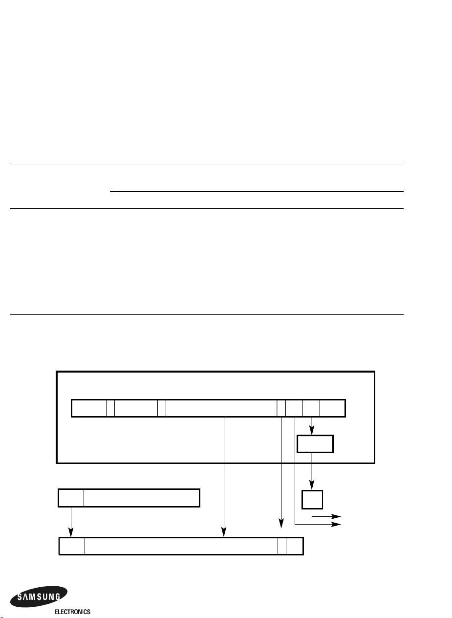
PCI Sparse Memory Space
The high-order ad<31:26> are obtained from either the hardware extension register
(HAE_MEM) or the 21164 address depending on sparse-space regions, as shown in
Table 1–7. See the Digital Semiconductor 21174 Core Logic Chip Technical Refer-
ence Manual for more information about the 21174 HAE_MEM CSR.
Table 1–7 PCI Address Mapping
21164
Address Region ad
<31> <30> <29> <28> <27> <26>
80.0000.0000
to
83.FFFF.FFFF
84.0000.0000
to
84.FFFF.FFFF
85.0000.0000
to
85.FFFF.FFFF
Figure 1–9 shows the mapping for region 1.
Figure 1–9 PCI Memory Sparse-Space Address Generation – Region 1
1 HAE_MEM
<31>
2 HAE_MEM
<15>
3 HAE_MEM
<7>
21164 Address
39 38
1
SBZ
HAE_MEM
<30>
HAE_MEM
<14>
HAE_MEM
<6>
34 33 05 04 03 02 00
35
0
HAE_MEM
<29>
HAE_MEM
<13>
HAE_MEM
<5>
PCI QW Address
CPU<33> CPU<32> CPU<31>
HAE_MEM
<12>
HAE_MEM
<4>
060708
21164
HAE_MEM CSR
31 29 28 00
31 02 01 00
29 28
03
0 0
HAE_MEM
<11>
HAE_MEM
<3>
int4_valid
4 3
CPU<31>
HAE_MEM
<2>
Length in Bytes
Byte Offset
PCI Address
LJ04265A.AI4
System Address Space A–21
Page 88
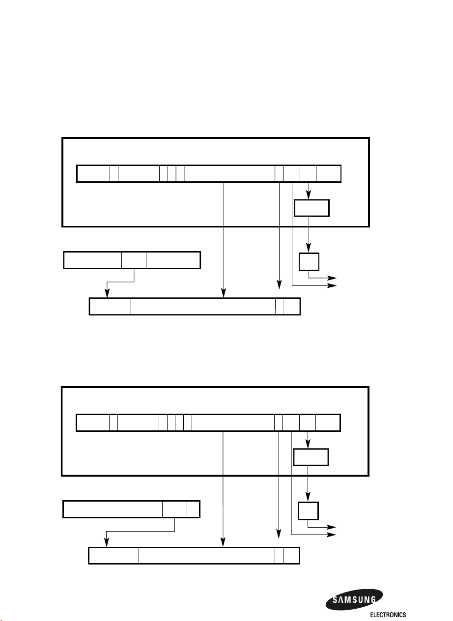
PCI Sparse Memory Space
Figure 1–10 shows the mapping for region 2.
Figure 1–10 PCI Memory Sparse-Space Address Generation – Region 2
21164 Address
39 38
SBZ
1
21164
HAE_MEM CSR
31 15
16 10 0011
31 02 01 00
27 26
PCI Address
34 33 05 04 03 02 00
32 31
35
0
0
1
PCI QW Address
060708
int4_valid
4 3
03
0 0
Length in Bytes
Byte Offset
LJ-04266.AI4
Figure 1–11 shows the mapping for region 3.
Figure 1–11 PCI Memory Sparse-Space Address Generation – Region 3
21164 Address
39 38
SBZ
1
21164
HAE_MEM CSR
31 07
31 02 01 00
PCI Address
A–22 System Address Space
35
34 33 05 04 03 02 00
32 31
30
010
1
08 01 0002
26 25
PCI QW Address
03
060708
int4_valid
4 3
Length in Bytes
Byte Offset
0 0
LJ-04267.AI4
Page 89

1.8 PCI Sparse I/O Space
The PCI sparse I/O space is divided into two regions — region A and region B.
Region A addresses the lower 32MB of PCI I/O space and is never relocated. This
region will be used to address the (E)ISA devices. Region B is used to address a further 32MB of PCI I/O space and is relocatable using the HAE_IO register.
A.8.1 Hardware Extension Register (HAE_IO)
In sparse space, the 21164 address bits <7:3> are used to encode byte enable bits,
size bits, and the low-order ad<2:0>. This means that there are now five fewer
address bits available to generate the PCI physical address.
The system provides two PCI sparse I/O space regions and allows one region to be
relocated by way of bits in the HAE_IO register.
A.8.2 PCI Sparse I/O Space Access Operation
The PCI sparse I/O space is located in the range 85.8000.0000 to 85.FFFF.FFFF.
This space has characteristics similar to the PCI sparse memory space. This 2GB
21164 address segment maps to two 32MB regions of PCI I/O address space. A read
or write transaction to this space causes a PCI I/O read or write command. The highorder PCI address bits are handled as follows:
PCI Sparse I/O Space
• Region A: This region has addr_h<34:30> = 10110 and addresses the lower
32MB of PCI sparse I/O space. Signals ad<31:25> are asserted at zero by the
hardware (see Figure 1–12). Region A is used to address (E)ISA address space
(the EISA 64KB I/O space cannot be relocated). Figure 1–12 shows PCI sparse
I/O space address translation in Region A.
• Region B: This region has addr_h<34:30> = 10111 and addresses a relocatable
32MB of PCI sparse I/O space. This 32MB segment is relocated by assigning
ad<31:25> to equal HAE_IO<31:25>. Figure 1–13 shows PCI sparse I/O space
address translation in Region B.
The remainder of the PCI I/O address is formed in the same way for both regions:
• ad<24:3> are derived from addr_h<29:8>.
• ad<2:0> are defined in Table 1–8.
System Address Space A–23
Page 90

PCI Sparse I/O Space
Table 1–8 contains the PCI sparse I/O space read/write encodings.
Table 1–8 PCI Sparse I/O Space Read/Write Encodings
Size Byte Offset
addr_h
<6:5>
21164
Instruction
Allowed ad<2:0>
PCI Byte
1
Enable
Data-In Register
Byte Lanes
63.....32 31.......0addr_h<4:3>
00 A<7>2,00 1110 OOOX
01 A<7>,00 1101 OOXO
Byte 00 10 LDL,STL A<7>,00 1011 OXOO
11 A<7>,00 0111 XOOO
00 A<7>,00 1100 OOXX
3
Word
01 01 LDL,STL A<7>,00 1001 OXXO
10 A<7>,00 0011 XXOO
00 A<7>,00 1000 OXXX
Tribyte 10 01 LDL,STL A<7>,00 0001 XXXO
Longword 11 00 LDL,STL A<7>,00 0000 XXXX
Quadword 11 11 LDQ,STQ 000 0000 XXXX XXXX
1
Byte enable set to 0 indicates that byte lane carries meaningful data.
2
A<7> = addr_h<7>.
3
Missing entries (for example, word size with 21164 address = 11) enjoy UNPREDICTABLE results.
A–24 System Address Space
Page 91
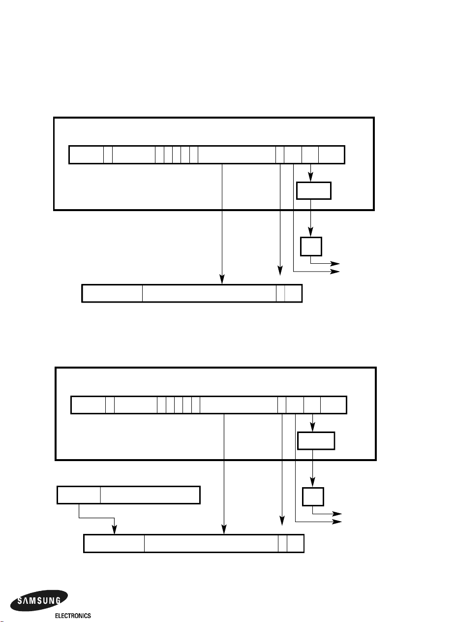
PCI Sparse I/O Space
Figure 1–12 PCI Sparse I/O Space Address Translation (Region A, Lower 32MB)
21164 Address
34 33 05 04 03 02 00
32 31
39 38
1
SBZ
35
1
30 29
0110
<29:8>
21164
31 02 01 00
0000000
PCI Address
25 24
060708
int4_valid
4 3
Length in Bytes
03
Byte Offset
0 0
LJ-04268.AI4
Figure 1–13 PCI Sparse I/O Space Address Translation (Region B, Higher Area)
21164 Address
39 38
1
SBZ
34 33 05 04 03 02 00
32 31
30 29
1
0111
060708
35
int4_valid
21164
HAE_IO CSR
31 24
25
4 3
Length in Bytes
31 02 01 00
25 24
03
Byte Offset
0 0
PCI Address
LJ04269A.AI4
System Address Space A–25
Page 92

PCI Configuration Space
1.9 PCI Configuration Space
The PCI configuration space is located in the range 87.0000.0000 to 87.1FFF.FFFF.
Software is advised to clear PYXIS_CTRL<FILL_ERR_EN> when probing for PCI
devices by way of configuration space read transactions. This will prevent the 21174
from generating an ECC error if no device responds to the configuration cycle (and
random data is picked up on the PCI bus).
A read or write transaction to this space causes a configuration read or write cycle on
the PCI. There are two classes of targets that are selected, based on the value of the
CFG register.
• Type 0 — These are targets on the primary 64-bit PCI bus. These targets are
selected by making CFG<1:0> = 0.
• Type 1 — These are targets on the secondary 32-bit PCI bus (that is, behind a
PCI-to-PCI bridge). These targets are selected by making CFG<1:0> = 1.
Note: CFG<1:0> = 10 or 11 are reserved (by the PCI specification).
Software must program the CFG register before running a configuration cycle.
Sparse address decoding is used. Signals addr_h<6:3> are used to generate both the
length of the PCI transaction in bytes and the byte enable bits. Signals ad<1:0> are
obtained from CFG<1:0>. Signals addr_h<28:7> correspond to ad<23:2> and provide the configuration command information (such as which device to select). The
high-order ad<31:24> are always zero.
Figure 1–14 depicts PCI configuration space (sparse). Figure 1–15 shows PCI configuration space (dense).
A–26 System Address Space
Page 93
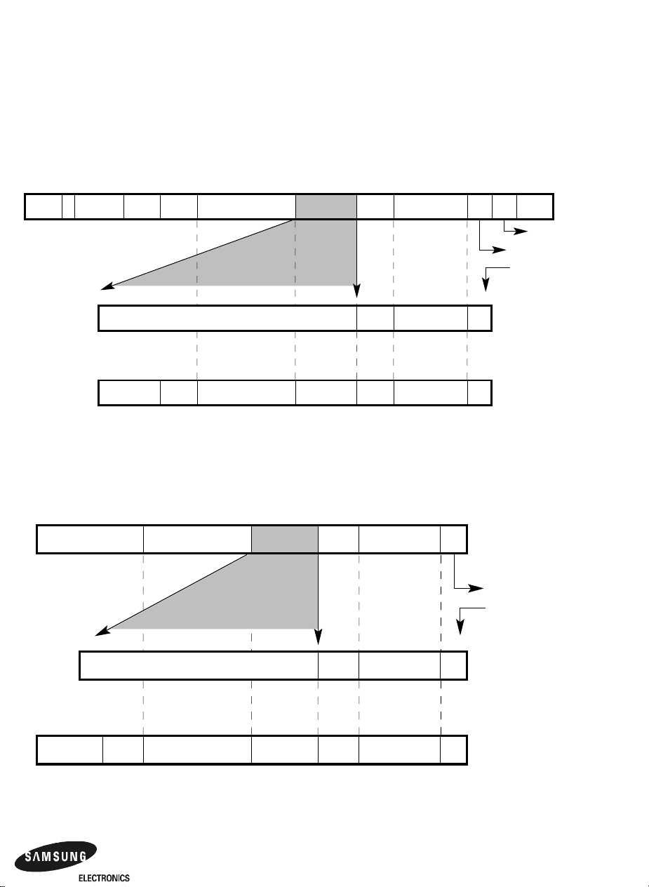
Figure 1–14 PCI Configuration Space Definition (Sparse)
PCI Configuration Space
CPU Address
313234353839 29 28 21 20 16 15 13 12 07 06 05 04 03 02
000111MBZ1
Type 0 PCI
Configuration
31 11 10 0708 02 01 00
IDSEL Function Register 0 0
Address
Type 1 PCI
Configuration
31 27 26 24 23 16 15 11 10 0708 02 01 00
000000 Bus Device Function Register 0 100
Address
Figure 1–15 PCI Configuration Space Definition (Dense)
31 24 16 15 07 02
00
Length
Byte Offset
CFG<1:0>
LJ04270A.AI4
00
0108101123
31 07 02 00
IDSEL Function Register
31 24 16 15 07 02 00
000000 Bus Device Function Register 0 100
01081011
010810112327 26
System Address Space A–27
Byte Offset
CFG<1:0>
LJ-05400.AI4
Page 94

PCI Configuration Space
Peripherals are selected during a PCI configuration cycle if the following three conditions are met:
1. Their IDSEL pin is asserted.
2. The PCI bus command indicates a configuration read or write.
3. Address bits <1:0> are 00.
Address bits <7:2> select a Dword (longword) register in the peripheral’s 256-byte
configuration address space. Transactions can use byte masks.
Peripherals that integrate multiple functional units (for example, SCSI and Ethernet)
can provide configuration space for each function. Address bits <10:8> can be
decoded by the peripheral to select one of eight functional units.
Signals ad<31:11> are available to generate the IDSEL bits (note that IDSEL bits
behind a PCI-to-PCI bridge are determined from the device field encoding of a type
1 access). The IDSEL pin of each device is connected to a unique PCI address bit
from ad<31:11>. The binary value of addr_h<20:16> is used to select which
ad<31:11> is asserted, as shown in Table A–9.
Table A–9 CPU Address to IDSEL Conversion
CPU Address <20:16> ad<31:11> – IDSEL
00000 0000 0000 0000 0000 0000 1
00001 0000 0000 0000 0000 0001 0
00010 0000 0000 0000 0000 0010 0
00011 0000 0000 0000 0000 0100 0
..... .... .... .... .... .... .
..... .... .... .... .... .... .
10011 0100 0000 0000 0000 0000 0
10100 1000 0000 0000 0000 0000 0
10101 0000 0000 0000 0000 0000 0
..... ...(No device selected)
..... —
11111 0000 0000 0000 0000 0000 0
A–28 System Address Space
Page 95

Note: If a quadword access is specified for the configuration cycle, then the
least significant bit of the register number field (such as ad<2>) must be
zero. Quadword transactions must access quadword aligned registers.
If the PCI cycle is a configuration read or write cycle but the ad<1:0> are 01 (that is,
a type 1 transfer), then a device on a hierarchical bus is being selected via a PCI-toPCI bridge. This cycle is accepted by the PCI-to-PCI bridge for propagation to its
secondary PCI bus. During this cycle, <23:16> selects a unique bus number, and
address <15:8> selects a device on that bus (typically decoded by the PCI-to-PCI
bridge to generate the secondary PCI address pattern for IDSEL). In addition,
address <7:2> selects a Dword (longword) in the device’s configuration space.
Table 1–10 contains the PCI configuration space read/write encodings.
Table 1–10 PCI Configuration Space Read/Write Encodings
PCI Configuration Space
Size Byte Offset
addr_h
<6:5>
21164
Instruction
Allowed ad<2:0>
PCI Byte
1
Enable
Data-In Register
Byte Lanes
63.....32 31.......0addr_h<4:3>
00 A<7>2,00 1110 OOOX
01 A<7>,00 1101 OOXO
Byte 00 10 LDL,STL A<7>,00 1011 OXOO
11 A<7>,00 0111 XOOO
00 A<7>,00 1100 OOXX
3
Word
01 01 LDL,STL A<7>,00 1001 OXXO
10 A<7>,00 0011 XXOO
00 A<7>,00 1000 OXXX
Tribyte 10 01 LDL,STL A<7>,00 0001 XXXO
Longword 11 00 LDL,STL A<7>,00 0000 XXXX
Quadword 11 11 LDQ,STQ 000 0000 XXXX XXXX
1
Byte enable set to 0 indicates that byte lane carries meaningful data.
2
A<7> = addr_h<7>.
3
Missing entries (for example, word size with addr_h<6:5> = 11) generate UNPREDICTABLE results.
Each PCI-to-PCI bridge can be configured via PCI configuration cycles on its primary
PCI interface. Configuration parameters in the PCI-to-PCI bridge will identify the bus
number for its secondary PCI interface and a range of bus numbers that may exist hier-
System Address Space A–29
Page 96
PCI Configuration Space
archically behind it. If the bus number of the configuration cycle matches the bus number of the bridge chip’s secondary PCI interface, it will accept the configuration cycle,
decode it, and generate a PCI configuration cycle with ad<1:0> = 00 on its secondary
PCI interface. If the bus number is within the range of bus numbers that may exist
hierarchically behind its secondary PCI interface, the bridge chip passes the PCI configuration cycle on unmodified (ad<1:0> = 01). It will be accepted by a bridge further
downstream. Figure 1–16 shows a typical PCI hierarchy. This is only one example of
how the 21174 can be used in a system design.
Figure 1–16 PCI Bus Hierarchy
Bcache
21164
PCI-to-(E)ISA
Bridge
(E)ISA
Bus
21174
ASIC
32-Bit
Slots
Memory
64-Bit PCI Bus
PCI-to-PCI
Bridge
Slot
Slot
Slot
Audio
64-Bit Slots
PCI
Graphics
Internal PCI
SCSI SCSI SCSI
Ethernet
A–30 System Address Space
LJ-05401.AI4
Page 97

PCI Special/Interrupt Cycles
1.10 PCI Special/Interrupt Cycles
PCI special/interrupt cycles are located in the range 87.2000.0000 to 87.3FFF.FFFF.
The Special cycle command provides a simple message broadcasting mechanism on
the PCI. The Intel processor uses this cycle to broadcast processor status; but in general it may be used for logical sideband signaling between PCI agents. The special
cycle contains no explicit destination address, but is broadcast to all agents. Each
receiving agent must determine if the message contained in the data field is applicable to it.
A write access in the range 87.2000.0000 to 87.3FFF.FFFF causes a special cycle on
the PCI. The 21164’s write data will be passed unmodified to the PCI. Software
must write the data in longword 0 of the hexword with the following fields:
• Bytes 0 and 1 contain the encoded message.
• Bytes 2 and 3 are message dependent (optional) data fields.
A read of the same address range will result in an Interrupt Acknowledge cycle on
the PCI and return the vector data provided by the PCI-EISA bridge to the 21164.
1.11 Hardware-Specific and Miscellaneous Register Space
These registers are located in the range 87.4000.0000 to 87.FFFF.FFFF.
Table A–11 lists the address map for the hardware-specific registers.
Table A–11 Hardware and Miscellaneous Address Map
CPU Address <39:28> Selected Region
1000 0111 0100 General control, diagnostic, performance monitoring, and
error logging registers
1000 0111 0101 Memory control registers
1000 0111 0110 PCI address translation (scatter-gather, windows, and so
on)
1000 0111 0111 Reserved
1000 0111 1000 Miscellaneous registers
1000 0111 1001 Power management registers
1000 0111 1010 Interrupt controller registers
1000 0111 11xx Flash ROM read/write space – for programming
System Address Space A–31
Page 98

PCI to Physical Memory Address
The address space here is a hardware-specific variant of sparse-space encoding. For
the CSRs, addr_h<27:6> specifies a longword address where addr_h<5:0> must be
zero. All the 21174 registers are accessed with a LW granularity. For more specific
details on the 21174 CSRs, see the Digital Semiconductor 21174 Core Logic Chip
Technical Reference Manual. For the flash ROM, addr_h<30:6> defines a byte
address. The fetched byte is always returned in the first byte lane (bits <7:0>).
1.12 PCI to Physical Memory Address
Incoming PCI addresses (32-bit or 64-bit) have to be mapped to the 21164 cached
memory space (8GB). The 21174 provides five programmable address windows that
control access of PCI peripherals to system memory.
The mapping from the PCI address to the physical address can be direct, direct
mapped (physical mapping with an address offset), or scatter-gather mapped
(virtual mapping). These five address windows are referred to as the PCI target
windows.
Window 4 maps directly, using the “Monster Window” with dual-address cycles
(DAC), where ad<33:0> equals addr_h<33:0>.
The following three registers are associated with windows <3:0>:
• Window base (W_BASE) register
• Window mask (W_MASK) register
• Translated base (T_BASE) register
In addition, there is an extra register associated with window 3 only. This is the window DAC register and is used for PCI 64-bit addressing (that is, the DAC mode).
The following text applies only to windows <3:0>.
The window mask register provides a mask corresponding to ad<31:20> of an
incoming PCI address. The size of each window can be programmed to be from
1MB to 4GB in powers of two, by masking bits of the incoming PCI address using
the window mask register, as shown in Table A–12. (Note that the mask field pattern
was chosen to speed up timing-critical logic circuits.)
A–32 System Address Space
Page 99

PCI to Physical Memory Address
Table A–12 shows the PCI target window mask fields.
Table A–12 PCI Target Window Mask Register Fields
PCI_MASK<31:20> Size of Window Value of n
0000 0000 0000 1MB 20
0000 0000 0001 2MB 21
0000 0000 0011 4MB 22
0000 0000 0111 8MB 23
0000 0000 1111 16MB 24
0000 0001 1111 32MB 25
0000 0011 1111 64MB 26
0000 0111 1111 128MB 27
0000 1111 1111 256MB 28
0001 1111 1111 512MB 29
0011 1111 1111 1GB 30
0111 1111 1111 2GB 31
1111 1111 1111 4GB 32
Otherwise UNPREDICTABLE —
1
Only the incoming ad<31:n> are compared with <31:n> of the window base register, as shown in
Figure 1–18. If n=32, no comparison is performed.
1
Based on the value of the window mask register, the unmasked bits of the incoming
PCI address are compared with the corresponding bits of each window’s window
base register. If one of the window base registers and the incoming PCI address
match, then the PCI address has hit the PCI target window. Otherwise, the PCI
address has missed the window. A window enable bit, W_EN, is provided in each
window’s window base register to allow windows to be independently enabled
(W_EN = 1) or disabled (W_EN = 0).
If a hit occurs in any of the four windows that are enabled, then the 21174 will
respond to the PCI cycle by asserting the signal devsel. The PCI target windows
must be programmed so that their address ranges do not overlap; otherwise, the
results are UNDEFINED.
System Address Space A–33
Page 100

PCI to Physical Memory Address
The window base address must be on a naturally aligned boundary address depend-
1
ing on the size of the window
. This rule is not particularly difficult to obey, because
the address space of any PCI device can be located anywhere in the PCI’s 4GB memory space, and this scheme is compatible with the PCI specification:
A PCI device specifies the amount of memory space it requires via the Base registers in its configuration space. The Base Address registers are implemented so
that the address space consumed by the device is a power of two in size, and is
naturally aligned on the size of the space consumed.
A PCI device need not use all the address range it consumes (that is, the size of the
PCI address window defined by the base address) and it does not need to respond to
unused portions of the address space. The one exception to this is a PCI bridge that
requires two additional registers (the base and limit address registers). These regis-
2
ters accurately specify the address space that the bridge device will respond to
and
are programmed by the power-on self-test (POST) code. The 21174, as a PCI host-
3
bridge device, does not have base and limit registers
, but does respond to all the
addresses defined by the window base register (that is, all addresses within a window).
Figure 1–17 shows how the DMA address ranges of a number of PCI devices are
accepted by the PCI-window ranges. PCI devices are allowed to have multiple DMA
address ranges, as shown for device 2. The example also shows that the window can
be larger than the corresponding device’s DMA address range, as shown for device
0. Device 1 and device 2 have address ranges that are accepted by one window.
Each window determines whether direct mapping or scatter-gather mapping is used
to access physical memory.
1 For example, a 4MB window cannot begin at address 1MB. It must start at addresses
4MB, 8MB, 12MB, ... .
2 A PCI bridge device responds to all addresses in the range: base ≤ address < limit.
3 Host-bridge devices, because they are under system control, are free to violate the rules.
A–34 System Address Space
 Loading...