

SamHop Microelectronics SDM8401 Datasheet
S DM8401
S amHop Microelec tronics C orp.
Augus t , 2002
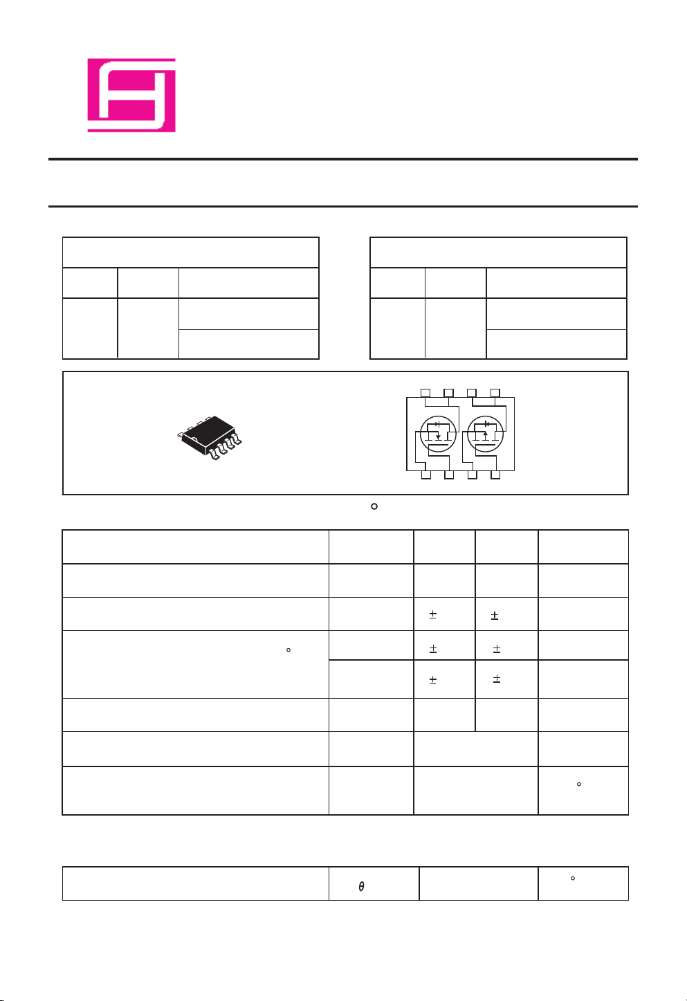
Dual E nhancement Mode Field E ffect T ransistor ( N and P C hannel)
PR ODUC T S UMMAR Y
VDS S
30V
ID
6A
S O-8
(N-C hannel)
R
DS (O N) ( m W ) T YP
18.5 @ VGS = 10V
25 @ VGS = 4.5V
1
PR ODUC T S UMMAR Y
VDS S
-30V
ID
-4.5A
D1 D1 D2 D2
8 7 6 5
1 2 3 4
S 1 G 1 S 2 G 2
ABS OLUT E MAX IMUM R ATINGS (TA=25 C unles s otherwise noted)
(P -C ha nnel)
R
DS (O N) ( m W ) T YP
38.5 @ VGS = -10V
57.5 @ VGS = -4.5V
P arameter
Drain-S ource Voltage
G ate-S ource Voltage
Drain C urrent-C ontinuous @ TJ=125 C
-P uls ed
Drain-S ource Diode F orward C urrent
Maximum P ower Dis s ipation
a
b
a
a
Opera ting J unction and S torage
Temperature R ange
THE R MAL C HAR AC TE R IS TIC S
Thermal R es is tance, J unction-to-Ambient
S ymbol
V
DS
V
G S
I
D
I
DM
I
S
P
D
TJ, T
S TG
a
R
J A
N-C ha nnel
30
20
6.0
18.0
1.7
-55 to 150
P -C hannel
-30
20
4.5
15
-1.7
2.0
62.5
Unit
V
V
A
A
A
W
C
C
/W
1
S DM8401
N-C hannel E L E C TR ICAL CHAR AC TE R IS TICS (TA 25 C unles s otherwis e noted)
P arameter
5
OF F C HAR AC TE R IS TIC S
Drain-S ource Breakdown Voltage
Zero G ate Voltage Drain C urrent
G ate-Body Leakage
ON C HAR AC T E R IS TIC S
G ate T hres hold Voltage
Drain-S ource On-S tate R es is tance
On-S tate Drain C urrent
S ymbol
B V
DS S
I
DS S
I
G S S
b
V
G S (th)
R
DS (ON)
I
D(ON)
g
F S
c
C ondition
V
G S
=
VDS 24V, V
V
G S
V
DS VG S
=
V
G S
V
G S
V
DS
V
DS
=
0V, ID 250uA
=
G S
= =
=
=
10V, I
4.5V, I
=
= 10V, V
= =
10V, I
0V
16V, VDS 0V
, ID = 250uA
=
D
9A
D
7A
=
G S
= 10V
D
20A
=
Typ
Min
30
1.5
1 3
18.5
25
40
16
C
Max
21
DYNAMIC C HAR AC T E R IS TIC S
1
100
32
Unit
V
uA
nA
V
m ohm
m ohm
A
SF orward Trans conductance
Input C apacitance
Output C apacitance
R evers e Transfer C apacitance
S WIT C HING C HAR AC TE R IS T IC S
Turn-O n Delay Time
R ise Time
Turn-O ff Delay Time
F a ll Time
Total G ate C harge
G ate-S ource C harge
G ate-Drain C harge
C
IS S
V
DS
=15V, V
G S
= 0V
C
OS S
C
R S S
c
t
D(ON)
t
r
t
D(OFF)
t
f
Q
g
Q
gs
Q
gd
f =1.0MH
Z
VDD = 15V,
ID = 1A,
V
G S
= 10V,
R
G E N
= 6
VDS =15V, ID =9A,V
VDS =15V, ID =9A,V
VDS =15V, ID = 9A,
V
G S
=10V
2
G S
=10V
G S
=4.5V
950
420
110
7
30
14
54
25.2
14.612.1
5.12
4.8
35
P
F
P
F
P
F
ns
ns
ns
ns
nC
nC
nC
nC

S DM8401
P-Channel E L E C TR ICAL C HAR ACTE R IS TICS (TA 25 C unles s otherwis e noted)
P arameter
S ymbol
=
C ondition
Min
Typ
C
Max
Unit
OF F C HAR AC TE R IS TIC S
Drain-S ource Breakdown Voltage
Zero G ate Voltage Drain C urrent
G ate-Body Leakage
ON C HAR AC T E R IS TIC S
b
G ate T hres hold Voltage
Drain-S ource On-S tate R es is tance
On-S tate Drain C urrent
0V, ID -250uA
B V
DS S
I
DS S
I
G S S
V
G S (th)
R
DS (ON)
I
D(ON)
g
F S
c
VDS -24V, V
V
G S
V
DS VG S
V
GS
V
GS
V
DS
V
DS
=
=
= =
=
=
=
=
= -5V, V
= =
G S
20V, VDS 0V
, ID = -250uA
=
-10V, I
D
-4.5V, I
D
=
G S
-15V, I
D
0V
=
-4.5A
-3.6A
= -10V
- 4.5A
-30
-1 -1.5 -3
-20
38.5
57.5
105
-1
100
53
95
V
m A
nA
V
m ohm
m ohm
A
SF orward Trans conductance
V
G S
DYNAMIC C HAR AC T E R IS TIC S
Input C apacitance
Output C apacitance
R evers e Transfer C apacitance
S WIT C HING C HAR AC TE R IS T IC S
Turn-O n Delay Time
R ise Time
Turn-O ff Delay Time
F a ll Time
Total G ate C harge
G ate-S ource C harge
G ate-Drain C harge
c
C
IS S
C
OS S
C
R S S
t
D(ON)
t
t
D(OFF)
t
Q
Q
Q
V
f =1.0MH
VD = -15V,
r
RL = 15
ID = -1A,
V
f
R
VDS=-15V,ID=-4.9A,V
g
VDS=-15V, ID=-4.9A,V
gs
gd
VDS =-15V, ID = - 4.9A,
V
3
DS
=-15V, V
G E N
= -10V,
G E N
= 6
G S
=-10V
P
P
P
ns
ns
ns
nC
nC
nC
nC
F
F
F
860
G S
= 0V
Z
457
140
20 ns
9
10 40
37
90
23 110
G S
=-10V
G S
=-4.5V
15
8
20
10
3
4
 Loading...