

S DM4952
S amHop Microelectronics C orp.
March , 2003
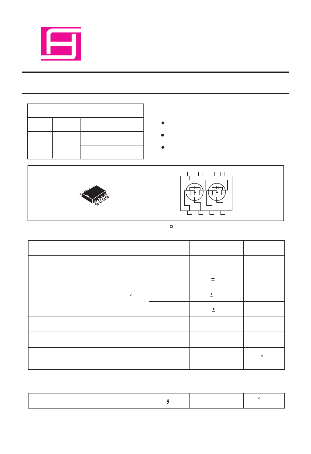
Dual P -C hannel E nhancement Mode F ield E ffect T ransistor
PR ODUC T S UMMAR Y
VDS S
-20V
ID
-5.3A
R DS (O N) ( m
50 @ V GS = -4.5V
75 @ V GS = -2.7V
S O-8
1
W
) MAX
AB S OLUTE MAXIMUM R ATING S (TA=25 C unles s otherwise noted)
F E ATUR E S
S uper high dens e cell design for low R
R ugged and reliable.
S urface Mount P ackage.
D1 D1 D2 D2
8 7 6 5
1 2 3 4
S 1
G 1
S 2
G 2
DS (O N
).
P arameter
Drain-S ource Voltage
G ate-S ource Voltage
Drain C urrent-C ontinuous @ TJ=125 C
-P ulsed
Drain-S ource Diode F orward C urrent
Maximum P ower Diss ipation
a
b
(300us P ulse Width)
a
a
Operating J unction and S torage
Tempera ture R ange
THE R MAL C HAR AC T E R IS TIC S
Thermal R es istance, J unction-to-Ambient
S ymbol
V
DS
V
G S
I
D
I
DM
I
S
P
D
TJ, T
S TG
a
R
J A
Limit Unit
-20
12
5.3
21
2.5
2
-55 to 150
62.5
V
V
A
A
A
W
C
C
/W
1
S DM4952
E LE C T R IC AL C HAR AC T E R IS T IC S (T A 25 C unles s otherwis e noted)
P arameter
S ymbol
=
C ondition
Min
Typ
OF F C HAR AC T E R IS TIC S
Drain-S ource B reakdown Voltage
Zero G ate Voltage Drain C urrent
G ate-B ody Leakage
ON C HAR AC T E R IS TIC S
b
G ate T hreshold Voltage
Drain-S ource On-S tate R es istance
On-S tate Drain C urrent
0V, ID -250uA
B V
DS S
I
DS S
I
G S S
V
G S (th)
R
DS (ON)
I
D(ON)
g
F S
c
VDS -16V, V
V
G S
V
DS VG S
V
GS
V
GS
V
DS
V
DS
=
=
= =
=
=
=
=
= -5V, V
= =
G S
12V, VDS 0V
, ID = -250uA
=
-4.5V, I
D
-2.7V, I
D
=
G S
-15V, I
D
0V
=
-2.9A
-1.5A
= -4.5V
- 4.9A
-20
-0.7
-20
13
V
G S
DY NAMIC C HAR AC T E R IS TIC S
C
Max
-1
100
50
75
Unit
V
uA
nA
V
m-ohm
m-ohm
A
SF orward Transconductance
Input C apacitance
Output C apacitance
R everse Transfer C apacitance
S WITC HING C HAR AC T E R IS TIC S
Turn-On Delay Time
R ise Time
Turn-Off Delay Time
F all Time
Total G ate C harge
G ate-S ource C harge
G ate-Dra in C harge
c
C
IS S
C
OS S
C
R S S
t
D(ON)
t
t
D(OF F)
t
Q
Q
Q
r
f
gs
gd
P
P
P
ns
ns
F
F
F
V
DS
=-10V, V
f =1.0MH
Z
VD = -10V,
RL =10 ohm
G S
= 0V
1190
700
250
19
18 70
40
ID = -1A,
120
V
G E N
= -4.5V,
R
G E N
=6 ohm
g
49
28 130
20
25
ns
ns
nC
VDS =-10V, ID = - 1A,
2
V
G S
=-4.5V
3.7
4.2
nC
nC

S DM4952
E LE C T R IC AL C HAR AC TE R IS TIC S (TA=25 C unles s otherwis e noted)
P a rameter
S ymbol
DR AIN-S OUR C E DIODE C HAR AC T E R IS TIC S
C ondition
b
Min
Typ
C
Max
Unit
5
Diode F orwa rd Voltage
V
S D
Notes
a.S urface Mounted on FR 4 B oard, t<= 10sec.
b.P ulse Tes t:P ulse W idth<= 300us , Duty C ycle<= 2%.
c.G uaranteed by design, not subject to production tes ting.
25
20
15
10
5
-ID , Drain C urrent (A)
0
0 0.5 1. 0 1.5 2. 0 2. 5 3.0
-V DS , D rain-to-S ource Voltage (V )
F igure 1. Output C haracteristics F igure 2. Transfer C hara cteristics
300 0
250 0
200 0
150 0
100 0
C , C apa citanc e (pF)
500
0
0
-V DS , D rain-to S ource V oltage (V)
F igure 3. C a pacitance
-VGS=10, 9,8, 7,6,5, 4,3V
5 10
-VGS=
2V
C iss
C oss
C rss
15 20
V
G S
= 0V, Is =-1. 7A
20
16
12
8
, Drain C urrent (A)
D
-I
4
0
0 0. 5 1 1 .5 2 2. 5 3
-V GS , Ga te-to-S ource V oltage (V)
1. 6
VGS=-4. 5V
I
D
=-2. 9A
1. 4
1. 2
1. 0
0. 8
On-R es istance(Ohms)
(N ormalized)
0. 6
R DS (O N),
0. 4
-50 0 50 10 0 125
-25
Tj, J unction Temperature ( C )
25
-55 C
25 C
75
-0.87
T j=125 C
T j( C)
F igure 4. On-R es istance Va riation with
Temperature
-1.2
V
3

S DM4952
1.3
VDS=V
1.2
1.1
1.0
0.9
0.8
-V th, Normalized
0.7
G ate-S ource T hreshold V oltage
0.6
-50 -25 0 25 50 7 5 100 125
Tj, J unction Temperature ( C )
G S
ID=-250uA
F igure 5. G a te T hres hold V a ria tion
with Temperature
25
20
15
10
1.15
1.10
1.05
1.00
0.95
0.90
-B VDS S , Normalized
0.85
Dra in-S ource B reakdown Voltage
-50 -25 0 25 50 75 100 12 5
Tj, J unction Temperature ( C )
ID=-250uA
F igure 6. B reakdown V oltage V ariation
with T empera ture
20. 0
V
G S
=0V
10. 0
5
gFS , T rans conductance (S )
0
0 5 10 15 20
-ID S, Dra in-S ource C urrent (A)
VDS=-15V
F igure 7. T rans conductance V a riation
with Dra in C urrent
5
VDS=-10V
ID=-1A
4
3
2
1
-V G S, G a te to S ource V oltage (V )
0
0 3 6 9 12 15 18 21
Qg, T otal G ate C harge ( nC )
F igure 9. G a te C harge
-Is , S ource-dra in current (A )
1.0
0.4 0.6 0.8 1.0 1.2 1.4
-V S D, B ody Diode F orward V oltage (V )
F igure 8. B ody Diode F orward Voltage
Variation with S ource C urrent
80
10
1
0.1
-ID , D rain C urrent (A)
0.03
0.1 1 10 20 50
t
imi
L
N)
(O
DS
R
DC
V
G S
=-10V
S ingle P ulse
TA=25 C
-V DS , D rain-S ource V oltage ( V )
100 m
1
10m
s
s
s
F igure 10. Maximum S afe
O perating Are a
3

S DM4952
DD
-V
on
t
d(off)
t
r
d(on)
R
IN
V
V
G S
G EN
R
G
L
D
OU T
V
S
t
OU T
V
IN
V
10%
t
90%
10% 10%
50% 50%
INVE R TE D
P ULS E W IDT H
90%
t
off
f
t
90%
F igure 11. S witching T est C ircuit
2
1
Duty C yc le=0.5
0. 2
0. 1
0. 1
0. 05
0. 01
0. 02
S ingle P ulse
-4
10
-3
10
r(t), Normalized E ffective
T rans ient Therma l Impeda nce
F igure 13. Normalized T hermal Trans ient Impedance C urve
F igure 12. S witching W a veforms
-2
10
S quare W ave P ulse Dura tion (s ec)
-1
10
DM
P
1
t
2
t
1. R thJA ( t)=r (t) * R thJA
2. R thJA=S ee Datas heet
3. TJ M-T A = PDM* R thJA (t)
4. Duty C ycle , D=t1/t2
1 10 100
5
 Loading...