

SamHop Microelectronics SDD3055L2, SDU3055L2 Datasheet
S DU/D3055L2
S amHop Microelectronics C orp.
Augus t , 20 02
N-C hannel E nhancement Mode Field E ffect Trans is tor
PR ODUC T SUMMAR Y
VDS S
20V
ID
15A
R DS (O N) ( m
34 @ V GS = 4. 5V
45 @ V GS = 2. 5V
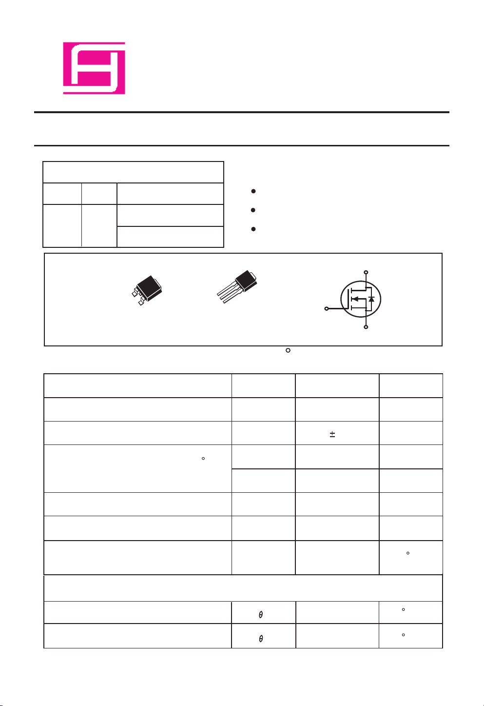
D
G
S
S DU S E RIE S
TO-252AA(D-PAK )
W
) TY P
G
D
S
S DD SE R IE S
TO-251(l-PA K)
AB S OLUT E MA XIMUM R AT ING S (TA=25 C unles s otherwis e noted)
F E ATUR E S
S uper high dense cell des ign for low R
R ugged and reliable.
TO-252 and T O -251 P ackage.
D
G
S
DS (O N
).
P arameter
Drain-S ource Voltage
G ate-S ource Voltage
Drain C urrent-C ontinuous @ TJ=125 C
-P ulsed
a
b
(300ms P uls e Width)
Drain-S ource Diode F orward C urrent
Maximum P ower Dissipation
a
Operating Junction and S torage
Temperature R ange
THE R MA L C HA R A C TE R IS TICS
Thermal R esistance, J unction-to-C ase
Thermal R esistance, J unction-to-Ambient
S ymbol
V
DS
V
G S
I
D
I
DM
a
P
TJ, T
R
R
I
S
D
S TG
J C
J A
Limit Unit
20
12
15
45
15
50
-55 to 150
3
50
V
V
A
A
A
W
C
C
C
/W
/W
1
S DU/D3055L2
E LE C TR IC AL C HAR AC TE R IS TIC S (T A 25 C unless otherwise noted)
P arameter
S ymbol
=
C ondition
Min
Typ
C
OF F C HAR AC T E R IS TIC S
Drain-S ource B reakdown Voltage
Zero G ate Voltage Drain C urrent
G ate-Body Leakage
ON C HAR AC T E R IS T IC S
b
G ate Threshold Voltage
Drain-S ource On-S tate R es is tance
On-S tate Drain C urrent
0V, ID 250uA
B V
DS S
I
DS S
I
G S S
V
G S (th)
R
DS (ON)
I
D(ON)
g
F S
c
VDS 20V, V
V
G S
V
DS VG S
V
G S
V
G S
V
DS
V
DS
=
=
= =
=
= 5V, V
G S
8V, VDS 0V
=
, ID = 250uA
=
=
= =
4.5V, I
2.5V, I
10V, I
D
D
G S
D
=
=
= 4.5V
0V
=
6.0A
5.2A
6.0A
20
0.7
20
34
45
17
V
G S
DYNAMIC C HAR AC TE R IS T ICS
Max
1
100
60
70
Unit
V
uA
nA
V
m-ohm
m-ohm
A
SF orward Transconductance
Input C apacitance
Output Capacitance
R evers e Trans fer C apacitance
S WIT C HING C HAR AC TE R IS T ICS
Turn-On Delay Time
R ise Time
Turn-Off Delay T ime
F all Time
Total G a te C harge
G ate-S ource Charge
G ate-Drain Charge
C
IS S
V
DS
=8V, V
G S
= 0V
C
OS S
C
R S S
c
t
D(ON)
t
r
t
D(OFF )
t
f
Q
g
Q
gs
Q
gd
f =1.0MH
Z
VDD = 10V,
ID = 1A,
V
G E N
= 4.5V,
RL = 10
R
GE N
= 6
ohm
ohm
VDS=10V,ID =6A,V
VDS=10V,ID =6A,V
VDS =10V, ID = 6A,
V
G S
=10V
2
G S
G S
=10V
=4.5V
705
280
65
10
15 30
35
20 40
25
9.3 11.5
2
2
P
P
P
20 ns
ns
ns
60
ns
30
nC
nC
nC
nC
F
F
F
 Loading...