

S DP /B55N03L
S amHop Microelectronics C orp.
S eptember , 2002
4
PR ODUC T S UMMAR Y
VDS S
30V
ID
55A
D
G
S
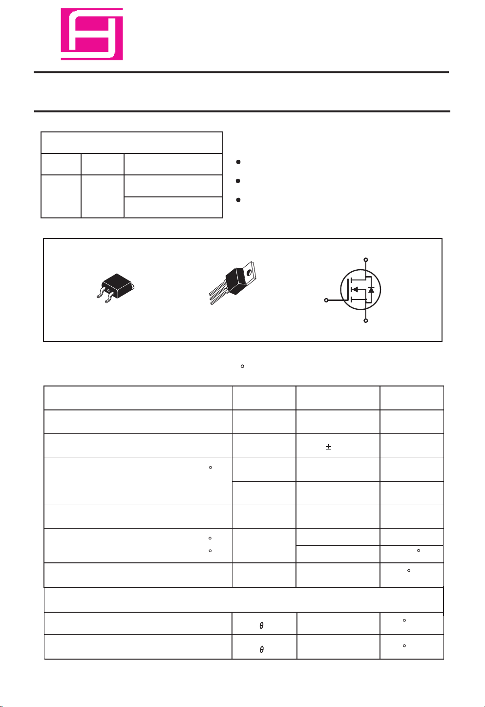
S DB S E RIE S
TO-2 63(DD-PAK)
R DS (on) ( m
12.5 @ VG S = 10V
20 @ VG S = 4.5V
W
)
TYP
G
D
S
F E ATUR E S
S DP S E RIE S
TO-2 20
S uper high dense cell design for extremely low R DS (ON).
High power and current handling capability.
TO-220 & TO-263 package.
D
G
S
ABS OLUTE MAX IMUM R ATING S (TC =25 C unless otherwise noted)
P arameter
Drain-S ource Voltage
S ymbol
V
DS
Limit Unit
30
V
G ate-S ource Voltage
Drain C urrent-C ontinuous @ TJ =125 C
-P ulsed
a
Drain-S ource Diode Forward C urrent
Maximum P ower Dissipation
@ T c=25 C
Derate above 25 C
Operating and S torage
Temperature R ange
THE R MAL C HAR AC TE R IS TIC S
Thermal R es is tance, J unction-to-C a s e
Thermal R es is tance, J unction-to-Ambient
V
I
P
TJ, T
R
R
G S
I
D
DM
I
S
D
1
S TG
J C
J A
20
55
140
55
75
0.5
-65 to 175
2.5
62.5
V
A
A
A
W
W / C
C
C
/W
C
/W
S DP /B55N03L
E LE C T R IC AL C H AR AC T E R IS T IC S (T C 25 C unless otherwis e noted)
4
P arameter
S ymbol
=
C ondition
OF F CHAR ACT E R IS T IC S
V
G S
Drain-S ource B reakdown Volta ge
Zero G ate Voltage Drain Current
G a te-Body Leakage
ON C HAR AC TE R IS TIC S
a
G a te T hres hold Voltage
Drain-S ource On-S tate R es istance
On-S ta te Drain C urrent
B V
DS S
I
DS S
I
G S S
V
G S (th)
R
DS (ON)
I
D(ON)
g
F S
b
0V, ID 250uA
=
VDS 24V, V
= =
V
G S
16V, VDS 0V
=
V
DS VG S
, ID = 250uA
=
V
G S =
10V, ID = 27A
V
GS =
4.5V, ID = 22A
V
G S
= 10V, V
V
DS =
10V, ID = 27A
=
G S
DS
0V
=
= 10V
DYNAMIC C HAR AC TE R IS TICS
Typ
Min
30
1 1.5 3
12.5
20
60
32
Max
10
100
14
23
Unit
V
uA
nA
V
m ohm
m ohm
A
SF orward Transconductance
Input C apacitance
Output C apacitance
R evers e Transfer C apacitance
S WIT C HING C HAR AC TE R IS TIC S
Turn-O n Delay Time
R ise Time
Turn-O ff Delay Time
F all Time
Total G ate Charge
G a te-S ource C harge
G a te-Drain C harge
P
C
IS S
V
DS
=15V, V
C
OS S
C
R S S
b
t
D(ON)
t
r
t
D(OFF)
t
f
f =1.0MH
VDD = 15V,
ID = 1A,
V
G S
= 10V,
R
G E N
VDS=15V, ID=27.5A,V
Q
g
VDS=15V, ID=27.5A,V
Q
Q
gs
gd
VDS =15V, ID = 27.5A,
V
G S
=10V
2
=60
Z
ohm
G S
= 0V
G S
G S
=10V
=4.5V
930
340
120
16 ns
17
23 250
37
90
20 200
26.1
13.7
35
16.5
5.4
4.6
F
P
F
P
F
ns
ns
ns
nC
nC
nC
nC
 Loading...