

SAMES SA9122EPA Datasheet
sames
V
SS
8
A
PC
1
PC
0
PC
PC
PC
PC
PC
PC
6
7
5
2
3
4
STB
CS
RST
WR
INT
ALE
RD
6
PD
6
PD
PD
PD
PD
PD
PD
4
5
0
1
3
2
PD
523
4
0
1
7
2
AD
SS
7
6
5
V
AD
AD
AD
4
3
AD
AD
345
021
6PE7VDD
7
1
AD
0
AD
FEATURES
SA9203/5
6/3 X 8 PORT EXPANDER
n Six (SA9203) or three (SA9205) 8-Bit
I/O Ports
n Each bit of one port independently
programmable as input or output
n Five (SA9203) or two (SA9205)
remaining ports can be individually
configured as input or output. (Direction
applicable to all 8 pins of each port.)
n One 8-Bit port programmable as either
atched or transparent inputs
n Supports byte-wide and bit-wide I/O
port addressing modes on all ports
DESCRIPTION
The SAMES SA9203/5 Port Expander is a
CMOS device suited to microprocessor
based applications requiring input/output
port expansion. The device interfaces very
simply to any microcontroller/microprocessor with a multiplexed address/data
bus structure.
The SA9203 includes 8 independently
programmable I/O pins for Port A and Port
B to F (5 ports) independently programmable
as I/O. It is packaged in a PCB efficient 68
pin PLCC package. The SA9205 includes
8 independently programmable I/O pins for
Port A with Port B and Port C as independently programmable I/O, packaged in a
cost effective 44 pin PLCC package.
n Readback of all control and port
registers
n Interfaces directly with multiplexed
address and data bus microprocessors/
microcontrollers
n Internal address latch
n Single +5V power supply
n Low power CMOS
n Completely static operation
n TTL-level compatibility
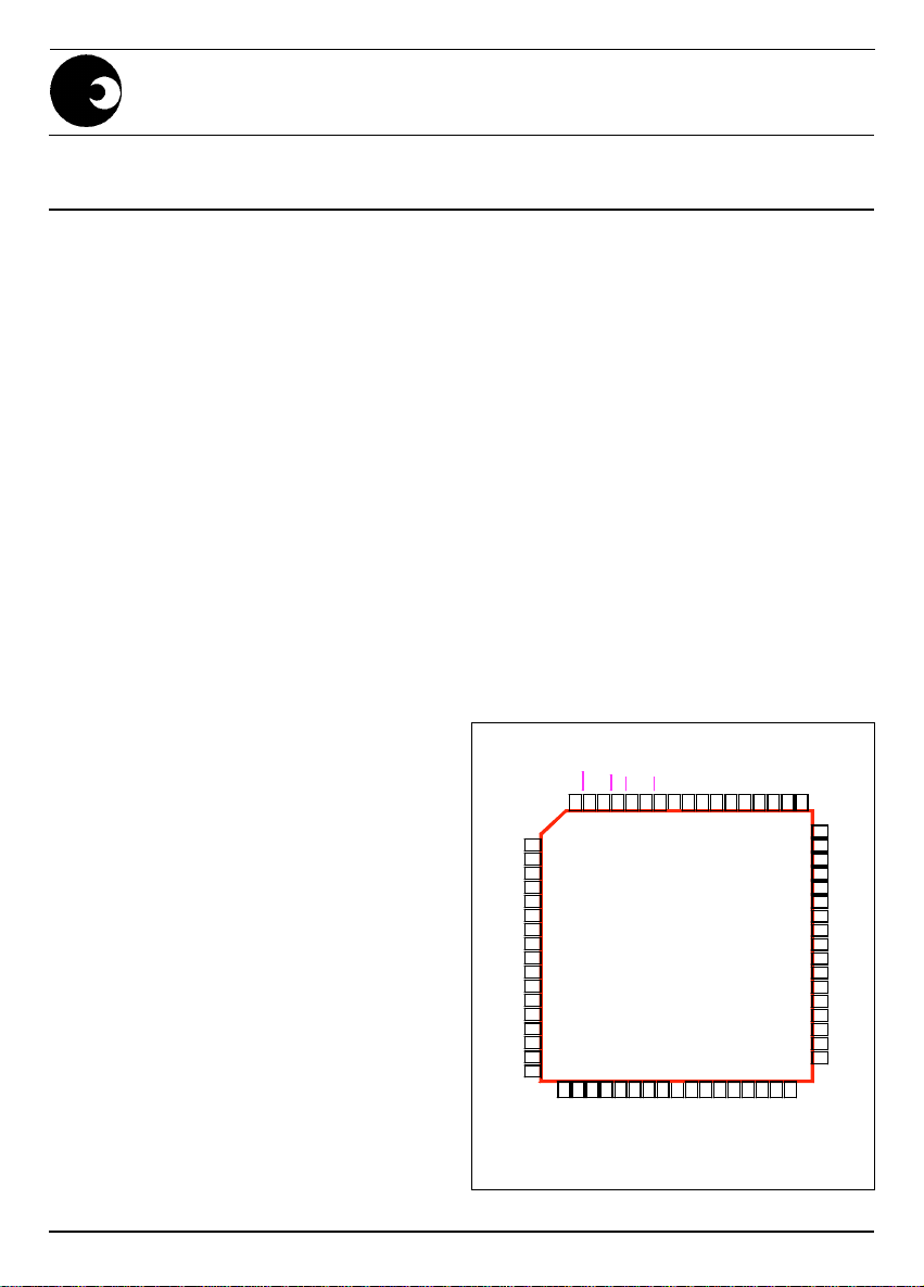
FIGURE 1: PIN CONNECTION FOR
SA9203
SA9203
33 34
32
31
2
1 6665646768
35
36 37 38 39
63
6162
PF
60
PF
59
PF
58
PF
57
PF
56
PF
55
PF
54
PF
53
52
51
PE
50
PE
49
PE
48
PE
47
PE
46
PE
45
PE
44
41
40
42
43
PA
10
0
PA
1
11
PA
12
2
PA
3
13
PA
4
14
PA
5
15
PA
6
16
PA
7
17
V
DD
18
PB
19
0
PB
20
1
PB
21
2
PB
22
3
PB
23
4
PB
5
24
PB
25
6
PB
26
7
DR-01266
9
876 543
28
27
29 30
4491
PDS039-SA9203/5-001 REV. A 20-08-96
1/14
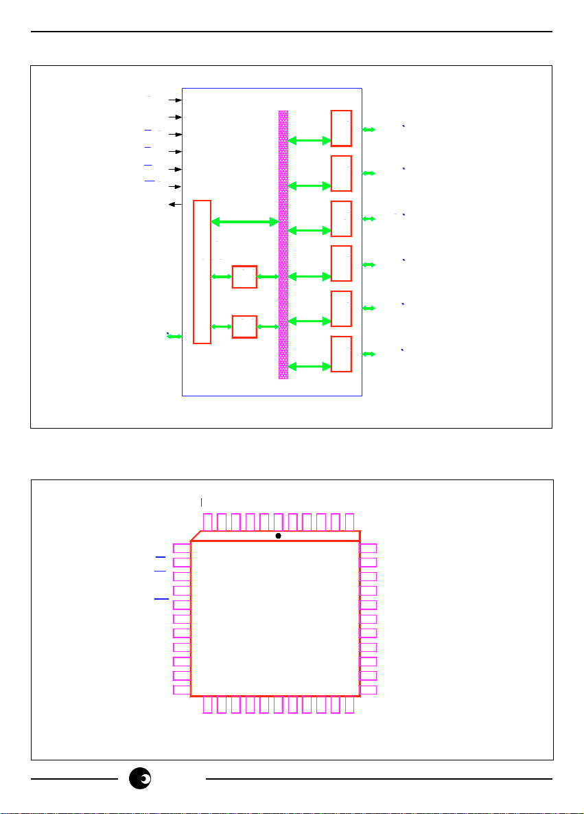
SA9203/5
Inter
face
AD(7:0
CON
PRTB
CON
PRTA
INT
RST
WR
ALE
CSRDSTBPPOR
F
POR
D
POR
E
PE(7:
PF(7:
PD(7:
POR
A
POR
C
POR
B
PC(7:
PA(7:
PB(7:
2
FIGURE 2: BLOCK DIAGRAM FOR SA9203
µµ
DR-01267
FIGURE 3: PIN CONNECTION FOR SA9205
CS
NC
AD
6
543
7
ALE
RD
8
WR
9
INT
10
RST
11
V
12
DD
STB
13
PA
14
0
PA
15
1
PA
16
2
PA
17
3
20 2119
18
4
5
6
PA
PA
PA
DR-01268
2/14
sames
7
5
6
AD
AD
SA9205
22
7
0
PA
PB
3
AD
26 27 28
2
PB
AD
3
PB
1
2
AD
4
PB
4
SS
AD
14344V42 41 40
23 2524
1
SS
V
PB
0
AD
5
PB
PC
39
7
PC
38
6
PC
37
5
PC
36
4
PC
35
3
V
34
DD
PC
33
2
PC
32
1
PC
31
0
PB
7
30
PB
29
6

FIGURE 4: BLOCK DIAGRAM FOR SA9205
STB
ALE
CS
RD
WR
RST
INT
µµ
P
Inter-
face
AD(7:0)
DR-01269
CON
PRTA
CON.
PRTBC
PORT
A
PORT
B
PORT
C
SA9203/5
PA(7:0)
PB(7:0)
PC(7:0)
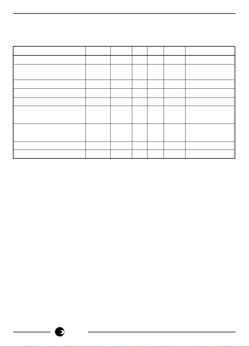
ABSOLUTE MAXIMUM RATINGS*
(All voltages are with respect to VSS)
Parameter Symbol Min Max Unit
Supply Voltage VDD-V
Voltage on any pin V
Current at any pin I
Storage Temperature T
M
STG
Operating Temperature T
SS
M
O
V
SS
7,0 V
VSS-0.3 VDD+0.3 V
100 mA
-40 +125 °C
0 +70 °C
* Stresses above those listed under “Absolute Maximum Ratings” may cause permanent
damage to the device. This is a stress rating only. Functional operation of the device
at these or any other condition above those indicated in the operational sections of this
specification, is not implied. Exposure to Absolute Maximum Ratings for extended
periods may affect device reliability.
sames
3/14
SA9203/5
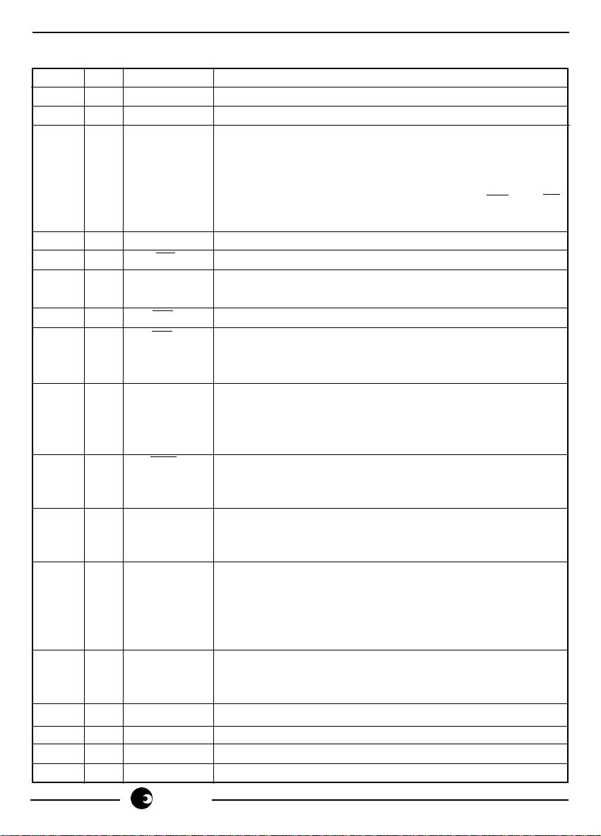
ELECTRICAL CHARACTERISTICS
(All measurements with respect to VSS, at 25°C, unless otherwise specified)
Parameters Symbol Min Typ Max Unit Condition
Supply Voltage V
Static Current I
DDS
4.75 5.0 5.25 V
DD
15 50 µA VDD = 5.0V
(See Note1)
Dynamic Current I
Input High Voltage V
Input Low Voltage V
Output High Voltage V
Output Low Voltage V
Input Leakage Current I
Tristate Leakage Current I
DDD
OH
OL
IN
TL
IH
IL
2.0 V VDD = 5.0V
4.5 4.7 V VDD = 5.0V
20 mA VDD = 5.0V
1.0 V VDD = 5.0V
I
= 5mA
OH
0.25 0.5 V VDD = 5.0V
I
= 5mA
OH
<1.0 3.0 µA VDD = 5.0V
<1.0 3.0 µA VDD = 5.0V
Note 1: All inputs tied to VDD or VSS with outputs not loaded.
Measurements made after RST applied.
4/14
sames
SA9203/5
PIN DESCRIPTION for SA9203
Pin Type Designation Description
18,52 VDD +5V Supply Input
1,35 VSS 0V ground Reference
61..68 I/O AD0..AD7 3-state address/data lines that interface with the CPU
lower 8-bit address/data bus. The 8-bit address is
latched into the SA9203 internal address latch on the
falling edge of ALE. The 8-bit data is respectively
written into and read out of the SA9203 on WR and RD
signals.
2 N/C Not connected.
3 I CS Active low input signal used to select the device.
4 I ALE This control signal latches the address on the AD0..7
lines on the falling edge of ALE.
5 I RD Input low on this line enables the data bus buffers.
6 I WR Input low on this line causes the data on the address/
data bus to be written to the I/O ports and, control
registers.
7 O INT If enabled via A.6, this output will be set (active edge
polarity programmed by D6 and output polarity
programmed via D7 of the Port B-F direction control
register) after data has been latched into PORT A.
8 I RST Input low on this line resets the chip and all internal
registers and all ports to input mode (The register
contents after a reset pulse will be described later).
9 I STB Input data on PORT A pins will be latched when STB is
active and transparent otherwise (polarity programmed
by D5 of the Port B-F direction control register)
10..17 I/O PA0..PA7 8 general purpose I/O pins comprising PORT A. This
port supports individual input or latched output
configuration of each pin. In addition,each pin of PORT
A selected as an input can be programmed to be
latched or transparent.
19..26 I/O PB0..PB7 8 general purpose I/O pins comprising PORT B. All 8
pins are programmed to be either latched outputs or
transparent inputs.
27..34 I/O PC0..PC7 Identical to PORT B
36..43 I/O PD0..PD7 Identical to PORT B
44..51 I/O PE0..PE7 Identical to PORT B
53..60 I/O PF0..PF7 Identical to PORT B
sames
5/14
 Loading...