

SAMES SA9101 Datasheet

sames
FEATURES
n Frame alignment/synthesis for PCM30
double frame and CRC-multiframe
format.
n Meets CCITT Rec.G704
n Interface to route selectable between
HDB3 and fibre optical
n HDB3 outputs switchable between fully
bauded and half bauded format
n Error checking via CRC4 procedure
n Insertion and extraction of alarms and
facility signals
n Selectable system - clock (4096 kHz/
8192 kHz)
n Selectable Interface mode (2048/4096
kBit/s) to system internal highway
n Programmable offsets for receive and
transmit data
n Two frame receive buffer for receive
route clock wander and jitter
compensation
n Slip detection and direction indication
n Extended HDB3 error detection
SA9101
PCM FRAME ALIGNER
n Error counters for code errors
(switchable to "Si zeros counter"), frame
errors and CRC4 errors
n Sub-multiframe assigned CRC Error
indication with possibility of automatic
insertion in Si-bit position of outgoing
multiframe.
n Simplified data transfer between
SA9101 and controller, supported by
data stacks for receive and transmit
signalling data, selectable interruptsources and DMA facilities.
n Double frame marker for serial data
extraction support
n Repeated transmission of signalling
data, if not updated.
n Three transparent modes for timeslot 0
in transmit direction
n Transparent mode for receive direction
n HDB3 error indication
n Idle channel data insertion selectable
for any timeslot
n Channel loopback capabilities, test and
diagnostic capabilities
n Parity checks
DESCRIPTION:
The SA9101 (Frame Alignment unit for PCM30 Systems) is a C-MOS device which
implements the interface to PCM30 Transmission Systems.
In the receive direction, the device performs HDB3 decoding, Frame alignment
(selectable between doubleframe and CRC-Multiframe) and extraction of signalling
data.
Wander absorption between the PCM carrier and the system internal highway is
performed using an internal 2 frame memory. The incoming data stream is monitored
and
M71-1797 PDS039-SA9101-001 REV.A 09-09-94
1/40
SA9101
Description (Cont.)
status and error conditions are reported through the µP interface. In the transmit
direction, Frame (and Multiframe) alignment, signalling data insertion and HDB3 coding
is performed.
If Multiframe format is enabled, CRC4 extraction and checking are carried out in the
receive direction and CRC4 data is inserted in the transmit direction.
Stacks for transmit and receive signalling data with DMA capability as well as maskable
interrupt sources simplify interfacing to microcontrollers.
Alarm simulation capabilities and selectable channel-loopback, support system
diagnostics.
Different transparent modes for timeslot 0 in transmit direction simplify system test and
data transmission through the system.
Advanced algorithms for synchronisation of doubleframe and CRC4 multiframe format
data, and monitoring of frame and doubleframe formats minimise loss of data.
Control Registers allow different control settings through the µP interface.
Advanced C-MOS Technology ensures low power consumption and high reliability.
The device is upwards compatible with the Siemens ACFA (PEB 2035 V4.1) in PCM30
mode.
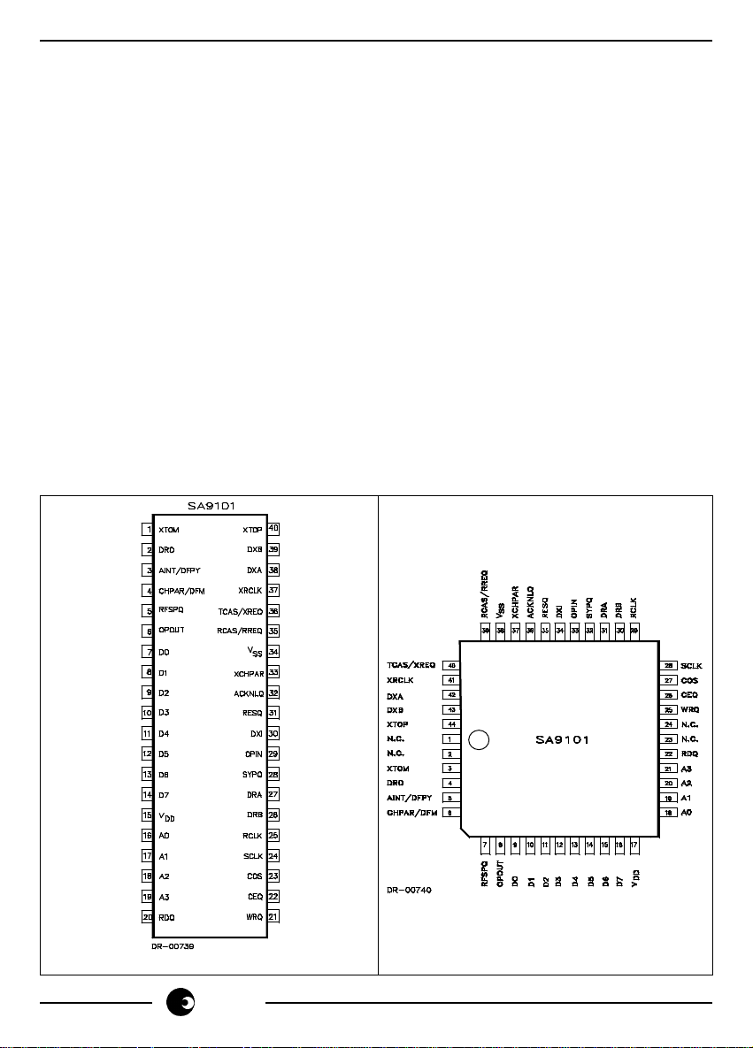
PIN CONNECTIONS
2/40
Package: DIP/DIC - 40 Package: PLCC - 44
sames
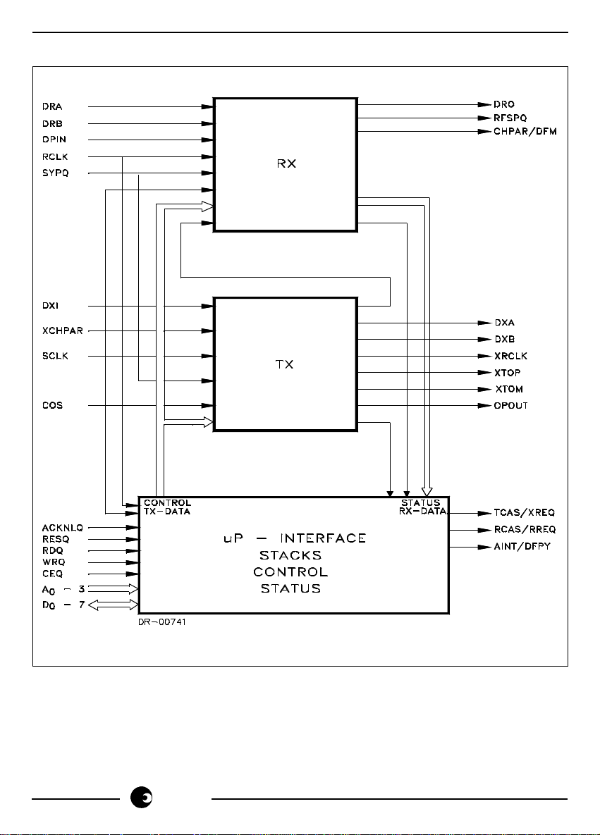
Block Diagram
SA9101
sames
3/40
SA9101
ELECTRICAL CHARACTERISTICS
Absolute Maximum Ratings*
Parameters Symbol Min Max Unit
Supply Voltage V
Voltage on any I/O pin V
Current on any I/O pin I
Storage Temperature T
Operating Temperature T
Package Power Dissipation P
*Stress above those listed under "Absolute Maximum Ratings" may cause permanent damage
to the device. This a stress rating only. Functional operation of the device at these or any other
condition above those indicated in the operational sections of this specification, is not implied.
Exposure to Absolute Maximum Ratings for extended periods may affect device reliability.
DC Operational Characteristics
= 5V, T = 10°C..+70°C
V
DD
Parameter Symbol Min. Max. Unit Remarks
Supply Voltage V
Supply Current (dynamic) I
Standby Current I
Inputs
High Voltage V
Low Voltage V
Leakage Current I
Input ACKNQ
Pullup Current -I
Outputs
High Voltage V
Low Voltage V
Bidirects
Input High Voltage V
Input Low Voltage V
Tristate Current I
Output High Voltage V
Output Low Voltage V
Operational Characteristics
= 25°C; V
T
A
= 5V ±5%; VSS = 0V
DD
Parameter Symbol Min. Max. Unit
Input capacitance C
Output capacitance C
I/O C
4/40
sames
DD
- V
I/VO
I/IO
STG
OP
D
SS
-0.3 6 V
-0.3 VDD+0.3 V
Limit Values
DD-VSS
DD
DDS
LEAK
PUP
OH
OL
LEAK
OH
OL
4.5 5.5 V
2.4 V
IH
IL
-5 5 µA VI=0..V
10 30 µA VI=0
2.8 V IOH=-1mA
2.4 V
IH
IL
-10 10 µA VI=0..V
2.8 V IOH=-1mA
Limit Values
IN
OUT
IO
20 mA
-55 +125 °C
-10 +70 °C
1000 mW
100 mA
100 µA
0.8 V
DD
0.4 V IOL=2mA
0.8 V
DD
0.4 V IOL=2mA
10 pF
15 pF
20 pF

PIN DESCRIPTION
SA9101
Pin Name Direction Description
Pin No.
DIL PLCC
AINT/DFPY O 3 5 Alarm interrupt/Double Frame Parity
ACKNLQ I 32 36 DMA Acknowledge
A[3-0] I 19-16 21-18 Address Bus
CEQ I 22 26 Chip Enable
CHPAR/DFM O 4 6 Receive Channel Parity/
Double Frame Marker
COS I 23 27 Carrier out of Service
DRA I 27 31 Receive Data in Plus
DRB I 26 30 Receive Data in Minus
DRO O 2 4 Receive Data Out
DXA O 38 42 Transmit Data Out Plus
DXB O 39 43 Transmit Data Out Minus
DXI I 30 34 Transmit Data In
D[7-0] B 14-7 16-9 Data Bus
OPIN I 29 33 Receive Optical Interface Data
OPOUT O 6 8 Transmit Optical Interface Data
RCAS/RREQ O 35 39 Receive TS16 Signal/Receive DMA
Interrupt Request
RCLK I 25 29 Receive Route Clock
RDQ I 20 22 Read Enable
RESQ I 31 35 Reset
RFSPQ O 5 7 Receive Frame Synchronisation
Pulse
SCLK I 24 28 System Clock
SYPQ I 28 32 Synchronisation Pulse
TCAS/XREQ O 36 40 Transmit TS16 Signal/Transmit DMA
Interrupt Request
V
DD
V
SS
S 15 17 +5V Supply
S 34 38 0V Ground
WRQ I 21 25 Write Enable
XCHPAR O 33 37 Transmit Channel Parity
XRCLK O 37 41 Transmit Route Clock
XTOM O 1 3 Test Data Output Minus
XTOP O 40 44 Test Data Output Plus
sames
5/40

SA9101
DESCRIPTION OF INTERFACES
Fibre Optical Interface
The fibre optical interface is enabled via the microprocessor interface.
Signal Pin Input/Output/Bidirect Function
OPIN 29 I Optical Fibre In
Unipolar Input Signal at 2048 kbps
Input polarity sense is programmable
via CR8B3. Latching of data is
performed with the falling edge of
RCLK if optical interface is selected
via CR1B2. (See Fig. 6 Line Interface
Timing.)
OPOUT 6 O Optical Fibre Out
Unipolar Output Signal at 2048 kbps
The output's active polarity is
programmable via CR6B7. Data is
clocked out on the rising edge of
XRCLK. Data duty cycle is 100%.
(See Fig. 6 Line Interface Timing.)
RCLK 25 I Route Clock
This clock, derived from the incoming
data by the line interface circuit (eg.
IPAT (PEB2235)), is necessary for
clocking received data into the SA9101.
XRCLK 37 O Transmit Route Clock
This 2048kHz clock is generated from
the Station Clock, SCLK. (See Fig. 5
System Interface Timing and Fig. 6
Line Interface Timing.)
PCM30 Interface
Signal P i n Input/Output/Bidirect Function
DRA 27, I Data Receive +/DRB 26 I HDB3 coded PCM Signal
DXA 38, O Data transmit +/DXB 39 O HDB3 coded PCM Signal
RCLK 25 I Route Clock f = 2.048 MHz
XRCLK 37 O Transmit route clock
6/40
sames

SA9101
Clock Generator
Signal Pin Input/Output/Bidirect Function
SCLK 24 I System Clock f=4,096 MHz/8,192MHz
RFSPQ 5 O Receive Frame Pulse
Frequency: 8 kHz
Duration: 488 ns
If loss of synchronisation, the line frame
pulse is inhibited
SYPQ 28 I Synchronous Pulse
Defines start of frame for System internal
data, together with the programmed offset
values of transmit and receive counter.
Pulse width: >244 ns
Period: Multiples of 125µs
DIU Controller
Signal Pin Input/Output/Bidirect Function
D0 - D7 7 - 14 B Bidirectional 8 bit data-bus
A0 - A3 16 - 19 I Address lines for SA9101 internal
registers
CEQ 22 I Chip enable input
WR Q 21 I Write enable input
RDQ 20 I Read enable input
COS 23 I Carrier out of service input.
SA9101 sends AIS to PCM30 interface
if input is at “1”
XREQ 36 O Transmit DMA interrupt request
RREQ 37 O Receive DMA interrupt request
AINT 3 O Alarm interrupt request
ACKNLQ 32 I DMA Acknowledge (Active Low)
(Not used when CR6B6 = 0. If not used
then pin must be fixed to V
internal TS16 signalling stacks is enabled
this input acts as an "access enable" to the
internal stacks (CRAB0-7 for T
SR7B0-7 for R
read/write command without the need of
) in conjunction with a
X
generating the chip enable signal at CEQ.
In this case it is to be connected to the
acknowledge output of the DMA controller.
.) If access to
DD
and
X
sames
7/40

SA9101
System Internal Highway
Signal Pin Input/Output/Bidirect Function
DRO 2 O Data Receive Out
DXI 30 I Data Transmit In
Timeslot channels 0 - 31 to/from PCM30 interface.
Bit rate 2048 kbit/s or 4096 kbit/s selectable via microprocessor interface.
CAS Processing
Signal Pin Input/Output/Bidirect Function
DRO 2 O Data Receive Out
DXI 30 I Data Transmit In
RCAS 35 O Receive CAS, active high marks
reception of channel 16
TCAS 36 O Transmit CAS, active high marks
transmission of channel 16
Test/Supervision
Signal Pin I nput/Output/Bidirect Function
CHPAR 4 O Receive Channel parity
Appears according to the related
channel (timeslot)
DFPAR 3 O Doubleframe Parity
During a current double-frame, the
parity of the previous double-frame
appears on DFPAR
XTOP 40, O HDB3-coded PCM (+), PCM (-) signal
XTOM 1 O for HDB3 diagnostic loop
RESQ 31 I Reset (Output Disable)
Asynchronous reset signal (active low),
resets the internal circuit and switches
all outputs to high impedance state -
must be held low for minimum of 2µs
XCHPAR 33 I Transmit channel parity
8/40
sames

SA9101
FUNCTIONAL DESCRIPTION
Receive path
Receive Link Interface
For data input, two different data types, with selectable input active polarity sense, are
supported:
- Dual rail data (PCM[+], PCM[-]) at ports DRA, DRB received from a Line Interface
Unit.
- Unipolar data at port OPIN (PCM 30) received from a fibre optical Interface.
Latching of data is carried out using the falling edge of the Receive route Clock
(RCLK, 2048 kHz) recovered from the PCM receive data stream. Dual rail data is
subsequently converted into a single rail, unipolar bit stream. The HDB3 line code
is used along with Double Violation Detection or Extended Code Violation Detection
(selectable). These errors increment the Code Violation Counter.
When using the unipolar input mode, the decoder is by-passed and no code violation
will be detected.
Additionally, the receive Link Interface comprises the alarm detection for AIS (Alarm
Indication Signal: unframed bit stream with constant logical ‘one’) and NOS (No
Signal: Input signal with insufficient bit rate or insufficient density of ones).
The single rail bit stream is then processed by the Receiver.
Receiver
The following functions are performed:
- Synchronization of pulse frame
- Synchronization of CRC4 multi-frame
- Error Indication when pulse frame synchronization is lost. In this case, AIS is sent to
the system side. If the receiver is in transparent mode, AIS is suppressed.
- Initiating and controlling of re-synchronization after loss of synchronization. This may
be carried out automatically by the SA9101, or under user control via the microprocessor
interface.
- Detection of Remote Alarm Indication from the incoming data stream.
- Separation of service bits and data link bits. This information is stored in special status
registers.
- Generation of control signals to synchronize the CRC checker, the parity generator,
and the Receive Speech Memory control unit.
If the multi-frame format is selected, CRC checking of the Incoming data stream is
done by generating check bits for a CRC submultiframe according to the CRC 4
procedure (PCM30, refer to CCITT Rec. G704). These bits are compared with those
check bits that are received during the next CRC sub-multiframe. If there is a
mismatch, the CRC error counter will be incremented. This 8-bit counter (default) can
be extended to 10-bit length, by writing to the control registers.
sames
9/40
SA9101
Receive Speech Memory
The speech memory is organized as a two-frame elastic buffer with a size of 64 x 9 bit
(8-bit channel data plus one parity bit).
The functions are:
- Compensation of Input wander and jitter. Maximum wander amplitude (peak-to-
peak) = 190 UI (1UI = 488 nS)
- Frame alignment between system frame and receive route frame
- Reporting and controlling of slips
Controlled by special signals generated by the Receiver, the unipolar bit stream is
converted into bit-parallel, channel-serial data which is circularly written to the speech
memory. At the same time, a parity signal is generated over each channel and also
stored in the speech memory.
Reading of stored data is controlled by the System Clock (SCLK) and the Synchronization
Pulse (SYPQ) in conjunction with the programmed offset values for the Receive timeslot/
Clock slot Counters. After conversion into a serial data stream and parity checking
(errors are reported via the status registers), the data is given out via port DRO. Channel
parity information is output at port CHPAR with selectable parity type (odd or even). Two
bit rates (2048/4096 kbps) are selectable via the microprocessor interface.
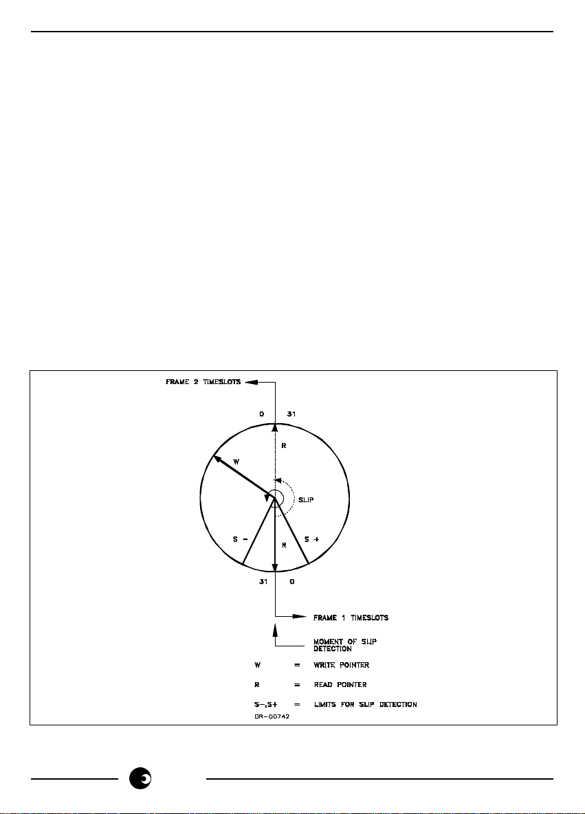
Figure 1.0: The Receive Speech Memory as circularly organized memory
10/40
sames

SA9101
Figure 1.0 illustrates the operation of the receive Speech Memory:
A slip condition is detected when the Write Pointer (W) and the Read pointer (R) of the
memory are nearly coincident, i.e. the Write pointer is within the Slip Limits (S+, S-). If
a slip condition is detected, a negative slip ( the next received frame is skipped) or a
positive slip (the previous received frame is read out twice) is performed at the System
Interface, depending on the difference between RCLK and SCLK, i.e. on the position of
pointer R and W within the memory.
To reduce delay, the Receive Speech Memory can be switched to one frame length. For
correct operation, System Clock SCLK and Synchronization Pulse SYPQ have to be
derived from the Receive Route Clock RCLK and the Receive Frame Synchronous Pulse
RFSPQ (PLL application). In Single Frame Mode, however, it is not possible to perform
a slip after the slip condition has been detected.
Receive Transparent Mode
If enabled, the frame aligner does not try to synchronise on the received data if
synchronisation is lost. The AIS to the System Interface is disabled. The data appears
on the System Interface synchronised to the System Clock (SCLK) as received.
Transmit path
The PCM data is received from the system internal highway at port DXI at 2048 kbps or
4096 kbps. The channel assignment is equivalent to the receive direction. Data in invalid
timeslots will be ignored.
Latching of data is controlled by the System Clock (SCLK) and the Synchronization Pulse
(SYPQ), in conjunction with the programmed offset values of the Transmit Timeslot/
Clockslot Counters.
The Transmit Route Clock (XRCLK) is derived directly from the system clock by an
internal clock divider. Consequently, the data received from the system interface is
switched through without the need of intermediate storage.
The parity generation/checking mechanism is symmetrical to the receive path. The
channel data is checked with the channel parity information generated internally or
externally (input at port XCHPAR with selectable parity type). Errors are reported to the
microprocessor interface. To avoid difficulties with external parity generation, the parity
signal for non-speech data (TS0 and TS16) is ignored.
Transmitter
The serial bit stream is then processed by the transmitter which has the following
functions:
- Frame/multiframe synthesis of one of the selectable framing formats
- Insertion of service and data link information.
- Remote Alarm generation
- CRC generation and insertion of CRC bits
sames
11/40

SA9101
Transmit Link Interface
Similar to the Receive Link Interface two different data types with selectable active
polarity for the output are supported:
- Dual rail data (PCM[+], PCM[-]) at ports DXA, DXB with selectable duty cycle (50%
or 100%) transmitted to a Line Interface Unit. Single rail data is converted into a dual
rail bit stream. The HDB3 line code is employed.
- Unipolar data at port OPOUT with 100% duty cycle transmitted to a fibre optical
interface.
Clocking of data is carried out on the positive transitions of the Transmit Route Clock:
XRCLK (2048 kHz). XRCLK is generated by the SA9101.
Additionally, the dual rail outputs XTOP and XTOM are provided for test applications.
Additional functions
Alarm Interrupt
Normally, the control of data transmission via the PCM line is carried out by polling the
internal status registers of the SA9101 at equal time intervals. However, for fast error
handling the option exists to configure a specific output port as interrupt port (AINT). This
signal may be connected to an interrupt input of the on-board processor. Triggering of
the output may be caused by up to 10 maskable interrupt sources.
Single Channel Loop Back
As one of the extended test options, the Single Channel Loop Back enables reflection
of a selected channel back to the system interface at port DRO.
TS16 Extraction/Insertion
TS16 data can be extracted/inserted via the µP or the DMA facility provided. For µP
interface, RREQ/XREQ act as interrupts. When one of these interrupts is received two
bytes must be read/written consecutively before next frame information is written into it.
For DMA operation see detailed timing diagram, Fig 7.3. (See DIU Controller Pin
description table, CR6B6 Register and SR5B5 Register descriptions.)
Data Extraction/Insertion is also possible through the serial ports DRO and DXI by using
a multiplexer in conjunction with the control signals RCAS/TCAS generated by the
SA9101.
Serial Data extraction on System Side
Together with the Double Frame Marker generated by the SA9101, any position in the
serial data can be pointed to, for extraction.
Idle Code Insertion
In TX direction any channel can be selected for idle code insertion using the Idle Channel
Register bank.
12/40
sames
 Loading...