

SAMES SA3488 Datasheet
sames
CMOS 256 X 256 DIGITAL SWITCHING MATRIX
FEATURES
■
Hardware (pin-to-pin) and software
compatible with M088 and M3488
■ 256 input and 256 output channel digital
switching matrix
■ Building block designed for large
capacity electronic exchanges, subsystems and PABX
■ Non-blocking single stage and higher
capacity blocks (512 or 1024 channels)
■ European and U.S. standard
compatible (32/24 serial channels per
frame)
■ PCM inputs and outputs mutually
compatible
SA3488
SA3488
■ Actual input-output channel
connections stored and modified via
an on chip 8-bit parallel microprocessor
interface
■ 6 main “Functions” or “Instructions”
available
■ Typical Bit Rate : 2Mbit/s
■ Typical Synchronization Rate : 8KHz
(time frame is 125µs)
■ 5V power supply with internally
generated bias voltage
■ MOS & TTL input/output levels
compatible
DESCRIPTION
The SA3488 is a non-blocking digital
switching matrix that is capable of routing
256 input channels to any of 256 output
channels. Data is fed into and out of the
device via eight serial PCM input and
output channels at 2MBits/sec. The device
can connect or disconnect each input
channel with any output channel, as well as
carry out other functions which are user
programmable via an eight bit parallel
microprocessor interface. The SA3488
sees its primary use as a building block in
high volume electronic exchanges, voice
data PABX and other standard data
communications applications. It can be
easily configured for operation in PCM 24
or PCM 30 formats.
SA3488
sames
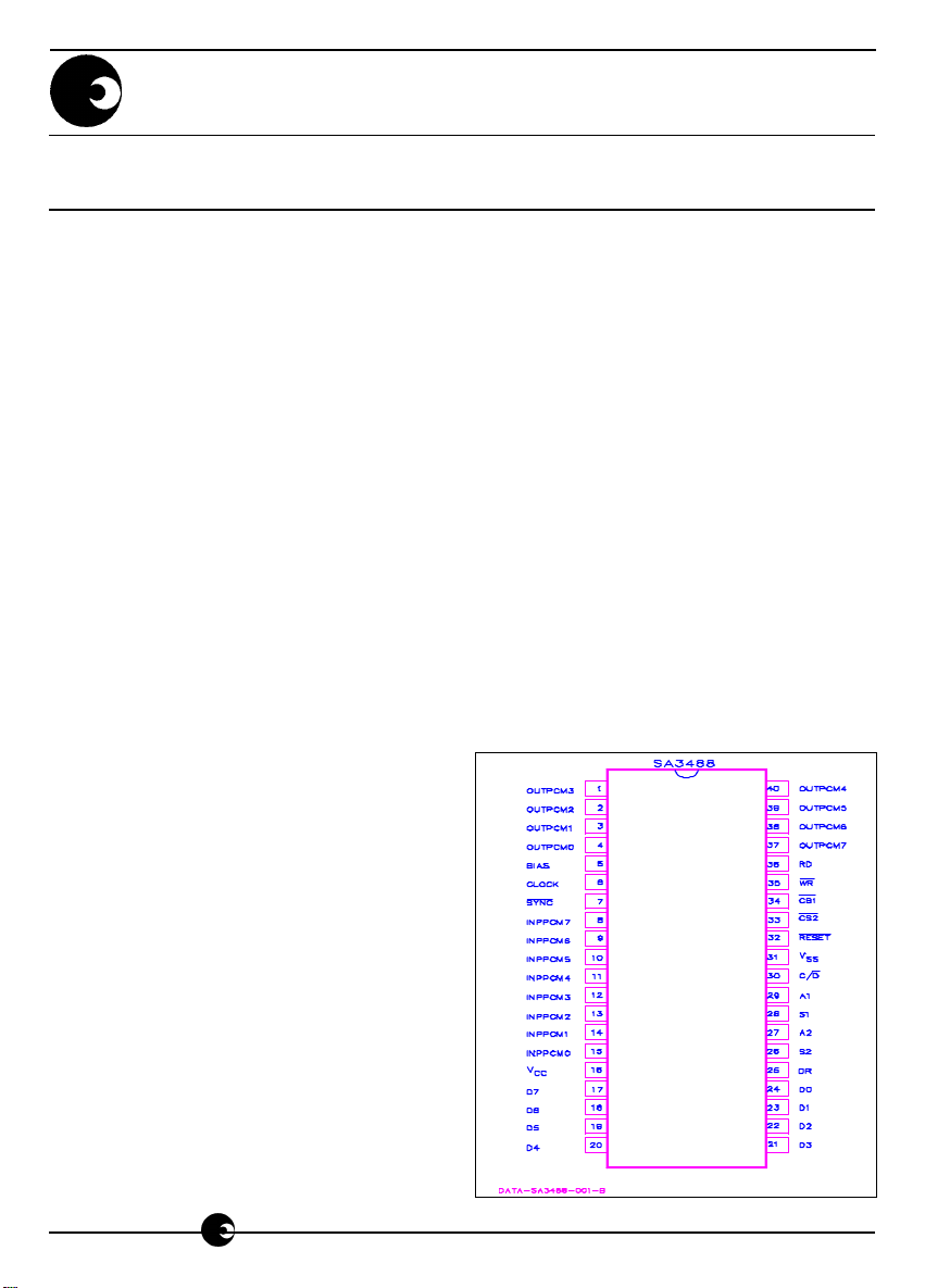
PIN CONNECTIONS:
1
SA3488
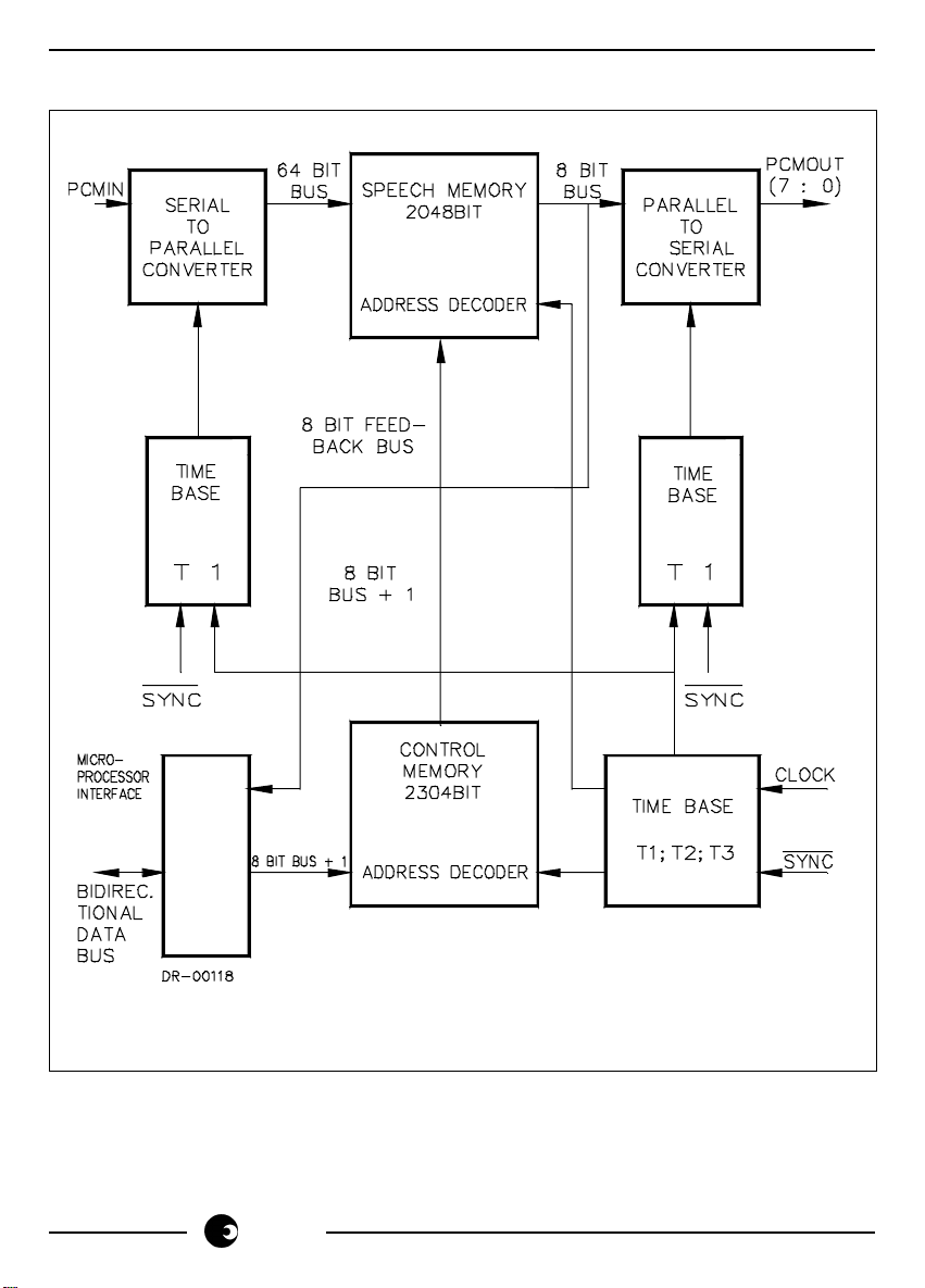
BLOCK DIAGRAM
sames
2
SA3488
ABSOLUTE MAXIMUM RATINGS *
Symbol Parameter Value Unit
V
CC
V
I
V
O
P
tot
T
stg
T
op
Supply Voltage -0.3 to 7 V
Input Voltage -0.3 to 7 V
Off State Output 7 V
Total Package Power Dissipation 1.5 W
Storage Temperature Range -40 to +125 °C
Operating Temperature Range 0 to +70 °C
* Stresses above those listed under “Absolute Maximum Ratings” may cause permanent damage
to the device. This is a stress rating only. Functional operation of the device at these or any other
condition above those indicated in the operation sections of this specification, is not implied.
Exposure to Absolute Maximum Ratings for extended periods may affect device reliability.
RECOMMENDED OPERATING CONDITIONS
Symbol Parameter Value Unit
V
CC
V
I
V
O
Supply Voltage 4.75 to 5.25 V
Input Voltage 0 to 5.25 V
Off State Input Voltage 0 to 5.25 V
CLOCK Freq. Input Clock Frequency 4.096 MHz
SYNC Freq. Input Synchronization 8 KHz
T
op
Operating Temperature 0 to 70 °C
CAPACITANCES (Measuring freq. = 1MHz; T
= 0 to 70°C; unused pins tied to VSS)
op
Symbol Parameter Pins Min. Typ. Max. Unit
C
I
C
I/0
C
0
Input Capacitance 6 to 15; 26 to 30; 32 to 36 5 pf
I/O Capacitance 20 to 24 15 pf
Output Capacitance 1 to 4; 17 to 19; 37 to 40 10 pf
sames
3

SA3488
D.C. ELECTRICAL CHARACTERISTICS (T
All D.C. characteristics are valid 250µs after V
= 0 to 70°C, V
amb
and clock have been applied.
CC
= 5V 5%)
CC
Symbol Parameter Pins Test Condition Min. Typ. Max. Unit
V
V
V
Clock Input Low Level 6 -0.3 0. 8 V
ILC
Clock Input High Level 6 2.4 V
IHC
Input Low Level 7 to 15 -0.3 0. 8
IL
20 to 24 V
CC
26 to 30
32 to 36
V
Input High Level 7 to 15 2.0 V
IH
CC
20 to 24 V
26 to 30
32 to 36
V
V
V
I
IL
Output Low Level 17 to 25 IOL = 1.8mA 0.4 V
OL
Output High Level 17 to 25 IOH = 250µA 2.4 V
OH
PCM Output Low Level 1 to 4 IOL = 2.0mA 0.4 V
OL
Input Leakage Current 6 to 15 V
37 to 40
26 to 30
= 0 to V
IN
CC
10 µA
32 to 36
I
DL
Data Bus Leakage 17 to 24 V
Current V
= 0 to V
IN
CC
and 36 tied to V
Device Initialization
CC
applied; Pins 35
CC
±10 µA
, after
V
I
CC
Supply Current 16 Clock Freq.= 4.096MHz 180 mA
sames
4
SA3488
A.C. ELECTRICAL CHARACTERISTICS (T
All A.C. characteristics are valid 250µs after V
capacitive load and R
the test pull up resistor.
L
= 0 to 70°C, VCC = 5V ±5%)
amb
and clock have been applied. CL is the max.
CC
Signal Symbol Parameter Test Condition Min. Typ. Max. Unit
CK t
(clock) t
SYNC t
PCM input t
Busses t
PCM t
Output referred to CK low level
Busses t
PDmin
PDmax
RESET t
WR t
t
RD t
t
Clock Period 230 ns
CK
Clock Low Level Width 100 ns
WL
t
Clock High Level Width 100 ns
WH
Rise Time 25 ns
t
R
t
Fall Time 25 ns
F
Low Level Setup Time 80 ns
SL
t
Low Level Hold Time 40 ns
HL
High Level Setup Time 80 ns
t
SH
t
High Level Width t
WH
Setup Time -5 ns
S
Hold Time 45 ns
H
CK
Propagation time CL = 50pf,RL=2K 45 ns
Propagation time CL = 50pf,RL=2K 200 ns
referred to CK high level
Low Level Setup Time 100 ns
SL
Low Level Hold Time 50 ns
t
HL
t
High Level Setup Time 90 ns
SH
t
High Level Width t
WH
Low Level Width 150 ns
WL
t
High Level Width t
WH
Repetition Interval t
REP
between Active Pulses + t
t
High Level Setup Time + t
SH
to Active Read Strobe
High Level Hold Time 20 ns
t
HH
from Active Read Strobe
Rise Time 60 ns
t
R
t
Fall Time 60 ns
F
Low Level Width 180 ns
WL
t
High Level Width t
WH
Repetition Interval t
REP
between Active Pulses + t
t
High Level Setup Time 0 ns
SH
to Active Read Strobe
High Level Hold Time 20 ns
t
HH
= 40+2 t
REP
WL(CK) +
R(CK)
= 40+2 t
REP
WL
+ t
CK +
CK
R
CK
CK
see
formula
0ns
CK
see
formula
from Active Write Strobe
t
Rise Time 60 ns
R
t
Fall Time 60 ns
F
ns
ns
ns
ns
sames
5
SA3488
A.C. ELECTRICAL CHARACTERISTICS (Cont.)
Signal Symbol Parameter Test Conditions Min. Typ. Max. Unit
CS1, t
CS2 to WR falling edge
C/D t
A1,S1, t
A2,S2 strobe end
(match t
inputs) strobe end
DR t
(data t
ready) from write strobe end Instructions 5, 5.t
SL(CS-WR)
t
HL(CS-WR)
t
SH(CS-WR)
t
HH(CS-WR)
t
SL(CS-RD)
t
HL(CS-RD)
t
SH(CS-RD)
t
HH(CS-RD)
S(C/D-WR)
t
H(C/D-WR)
t
S(C/D-WR)
t
H(C/D-WR)
S(match-WR)
H(match-WR)
t
S(match-RD)
t
H(match-RD)
W
PD
Low level setup time Active Case 0 ns
Low level hold time Active Case 0 ns
from WR rising edge
High level setup time Inactive Case 0 ns
to WR falling edge
High level hold time Inactive Case 0 ns
from WR rising edge
Low level setup time Active Case 0 ns
to RD falling edge
Low level hold time Active Case 0 ns
from RD rising edge
High level setup time Inactive Case 0 ns
to RD falling edge
High level hold time Inactive Case 0 ns
from RD rising edge
Setup time to write
strobe end 130 ns
Hold time from
write strobe end 25 ns
Setup time to read
strobe start 20 ns
Hold time from read
strobe end 25 ns
Setup time to write 130 ns
Hold time from 25 ns
Setup time to read 20 ns
strobe start
Hold time from read 25 ns
strobe end
Low state width Instructions 5,6 2 t
DR output delay
(active command) CL= 50pf ns
CK
14 t
CK
CK
ns
sames
6
 Loading...