

SAMES SA2005PPA, SA2005PSA Datasheet
Programmable Three Phase Power / Energy Metering
IC for Stepper Motor / Impulse Counter Applications
SA2005P
FEATURES
+ Direct drive for electro-mechanical counters or stepper
motors
+ Calibration and setup stored on external EEPROM - no
trim-pots required
+ Flexible programmable features providing ease of
implementation for meter manufacturers
+ Per phase energy direction and voltage fail indication
+ Precision oscillator on chip
DESCRIPTION
The SAMES SA2005P provides a single chip active energy
metering solution for three phase mechanical counter-based
meter designs.
Th SA2005P does not require any external trim-pots or resistor
ladders for meter calibration. Calibration and meter
configuration information is stored on a small external
EEPROM.
Meter setup stored on the EEPROM includes various metering
direction modes (total sum, absolute sum, positive or negative
energy) phase calibration data, rated metering conditions,
LED pulse rate, counter pulse width, counter resolution and
creep current.
samessames
+ Meets the IEC 521/1036 Specification requirements for
Class 1 AC Watt hour meters
+ Operates over a wide temperature range
+ Easily adaptable to different signal levels
+ Adaptable to different types of sensors
+ Precision voltage reference on-chip
+ Protected against ESD
A programmable rate pulse output is available for meter
calibration purposes. Per phase voltage fail and voltage
sequence faults as well as energy direction indication are
available as LED outputs. Programmable dividers enable
various mechanical counter or stepper motor counter
resolutions.
A precision oscillator, that replaces an external crystal, is
integrated on chip. A voltage reference is integrated on chip.
The SA2005P integrated circuit is available in 24-pin dual in
line plastic (DIP-24) and small outline (SOIC-24) package
options.
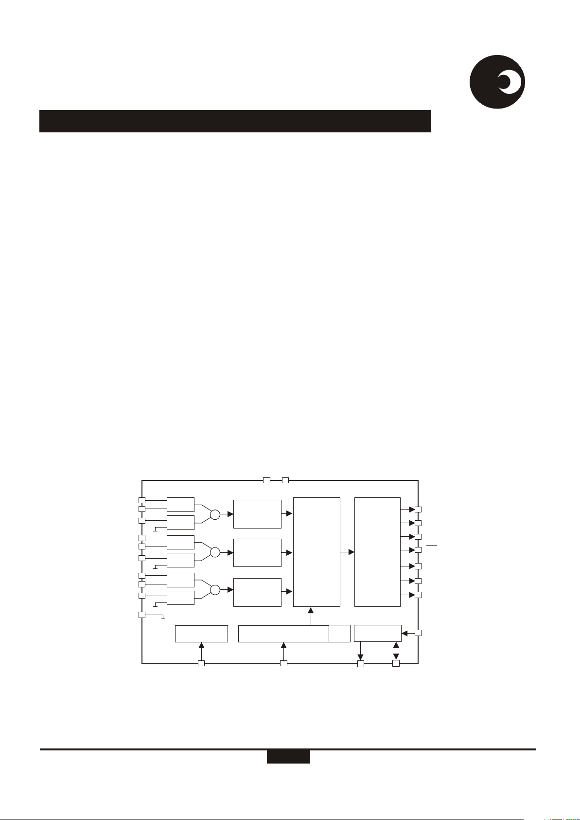
IIN1
IIP1
IVN1
IIN2
IIP2
IVN2
IIN3
IIP3
IVN3
GND
dr-01605
I1
V1
I2
V2
I3
V3
REF
VREF
X
X
X
VDD VSS
CHANNEL
BALANCE
PROG.
CHANNEL
ADDER
BALANCE
CHANNEL
BALANCE
TIMING & CONTROL
Figure 1: Block diagram
PROGRAM-
MABLE
ADDER
TEST
OSC
POWER
TO
PULSE
RATE
INTERFACE
SCL
LED
MON
MOP
PH / DIR
PH1
PH2
PH3
RLOAD
SDA
SPEC-0086 (REV. 2)
1/16
07-02-01
SA2005P
samessames
ELECTRICAL CHARACTERISTICS
(V = 2.5V, V = -2.5V, over the temperature range -10°C to +70°C , unless otherwise specified.)
DD SS
Parameter
Operating temp. Range
Supply Voltage: Positive
Supply Voltage: Negative
Supply Current: Positive
Supply Current: Negative
Symbol
T
O
V
DD
V
SS
I
DD
I
SS
Min
-25
2.25
-2.75 -2.25
#
Typ
Max
+85
2.75
15
15
16
16
Current Sensor Inputs (Differential)
Input Current Range
I
II
-25
+25
Voltage Sensor Input (Asymmetrical)
Input Current Range
Pin VREF
Ref. Current
Ref. Voltage
I
IV
-I
R
V
R
-25
45
1.1
50
+25
55
1.3
Digital I/O
Pins RLOAD, TEST, SDA
Input High Voltage
Input Low Voltage
V
IH
V
IL
V-1
DD
V+1
SS
Pins MOP, MON, LED, SCL,
PH/DIR, PH1, PH2, PH3
Output High Voltage
Output Low Voltage
V
OH
V
OL
V-1
DD
V+1
SS
Pin SDA
Pull up current
-I
IL
24
54 µA
Unit
°C
V
V
mA
mA
µA
µA
µA
V
V
V
V
V
Condition
Peak value
Peak value
With R = 24kW
connected to V
Reference to V
I = -2mA
OH
I = 5mA
OL
V = V
ISS
SS
SS
Pins TEST, RLOAD
Pull down current
I
IH
48 110 µA
V = V
IDD
#Extended Operating Temperature Range available on request.
ABSOLUTE MAXIMUM RATINGS*
Parameter Symbol Min Max Unit
Supply Voltage V -V -0.3 6.0 V
Current on any pin I -150 +150 mA
Storage Temperature T -40 +125 °C
Operating Temperature T -40 +85 °C
*Stresses above those listed under “Absolute Maximum Ratings” may cause permanent damage to the device. This is a stress
rating only. Functional operation of the device at these or any other condition above those indicated in the operational sections of
this specification, is not implied. Exposure to Absolute Maximum Ratings for extended periods may affect device reliability.
http://www.sames.co.za
DD SS
PIN
STG
O
2/16
SA2005P
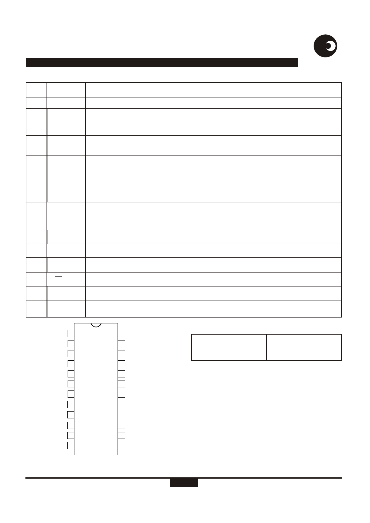
PIN DESCRIPTION
Designation Description
PIN
samessames
20
6
18
21, 24,
3
23, 22,
2, 1,
5, 4
19
8
9
17
10
11, 12
13
GND
V
DD
V
SS
IVN1, IVN2,
IVN3
IIN1, IIP1,
IIN2, IIP2,
IIN3, IIP3
VREF
SCL
SDA
TEST
LED
MON, MOP
PH / DIR
Analog Ground. The voltage to this pin should be mid-way between V and V .
DD SS
Positive supply voltage. Typically +5V if a current transformer is used for current sensing.
Negative supply voltage. Typically 0V if a current transformer is used for current sensing.
Voltage sense inputs. The current into the A/D converter should be set at 14µA at nominal mains
RMS
voltage. The voltage sense input saturates at an input current of ±25µA peak.
Inputs for current sensors. The termination resistor voltage from each current transformer is
converted to a current of 16µA at rated conditions. The current sense input saturates at an input
RMS
current of ±25µA peak.
This pin provides the connection for the reference current setting resistor. A 24kW resistor
connected to V sets the optimum operating condition.
SS
Serial clock output. This output is used to strobe data from the external EEPROM.
Serial data. Send and receive data from an external EEPROM.
Test input. For normal operation connect this pin to V .
SS
Calibration LED output. Refer to section Led Output (LED) for the pulse rate output options.
Motor pulse outputs. These outputs can be used to drive an impulse counter or stepper motor directly.
Multiplexed phase or direction driver output.
7
14, 15,
16
RLOAD
PH1, PH2,
PH3
1IIP2 IVN2
IIN2 IIN1
2
3
IVN3 IIP1
IIP3
4
IIN3
5
VDD
6 19
RLOAD
SCL
SDA
LED
MON
MOP
7
8
9
10
11
12
Triggers a data reload from the external EEPROM.
Multiplexed LED drivers for direction and mains fail indication.
24
23
22
IVN1
21
GND
20
VREF
VSS
18
TEST
17
PH3
16
PH2
15
PH1
14
PH / DIR
13
dr-01602
Figure 2: Pin connections: Package: DIP-24, SOIC-24
ORDERING INFORMATION
Part Number
SA2005PPA
SA2005PSA
Package
DIP-24
SOIC-24
http://www.sames.co.za
3/16
SA2005P
FUNCTIONAL DESCRIPTION
The SAMES SA2005P is a CMOS mixed signal analog/digital
integrated circuit that performs three phase power/energy
calculations across a power range of 1000:1 to an overall
accuracy of better than Class 1.
The integrated circuit includes all the required functions for 3phase power and energy measurement such as oversampling
A/D converters for the voltage and current sense inputs, power
calculation and energy integration. Internal offsets are
eliminated through the use of cancellation procedures.
samessames
operation of the meter. Every data byte stored in the EEPROM
is protected with a checksum byte to ensure data integrity.
ELECTROSTATIC DISCHARGE (ESD) PROTECTION
The SA2005P integrated circuit's inputs/outputs are protected
against ESD.
POWER CONSUMPTION
The overall power consumption rating of the SA2005P
integrated circuit is less than 80mW with a 5V supply.
The integrated circuit includes all the required functions for a
three phase mechanical counter-based meter design. A
precision oscillator, that replaces an external crystal, is
integrated on chip providing a temperature stable time base for
the digital circuitry. A temperature stable voltage reference
integrated on chip generates the reference current used by the
analog circuitry.
Voltage and currents are sampled simultaneously by means of
a sigma delta modulator type ADC and power is calculated for
each individual phase. A programmable channel balance on
each channel is used for individual channel calibration.
The scaled power is fed to a programmable adder that allows
the representation of the measured energy to be either total
sum or absolute sum.
The summed power is integrated and divided down to
represent integrated energy. Pulses on the LED output and on
the mechanical counter outputs represent measured amounts
of energy. The programmable dividers provide flexible counter
and calibration LED resolutions.
Outputs for phase voltage fail and voltage sequence faults and
energy direction are available.
The SA2005P does not require any external trim-pots or
resistor ladders as meter calibration and configuration data is
stored on a small external EEPROM. The SA2005P configures
itself from the EEPROM during power up. These features
enables meter manufacturers flexible meter designs from a
single integrated circuit.
AUTOMATIC DEVICE CONFIGURATION (BOOT UP)
During power up, registers containing configuration and
calibration information is updated from an external EEPROM.
The device itself never writes tot he EEPROM so any write
protect features offered by manufacturer of EEPROM’s may
be used to protect the configuration and calibration constant of
the meter. The device reloads its configuration every 1193
seconds from the external EEPROM in order to ensure correct
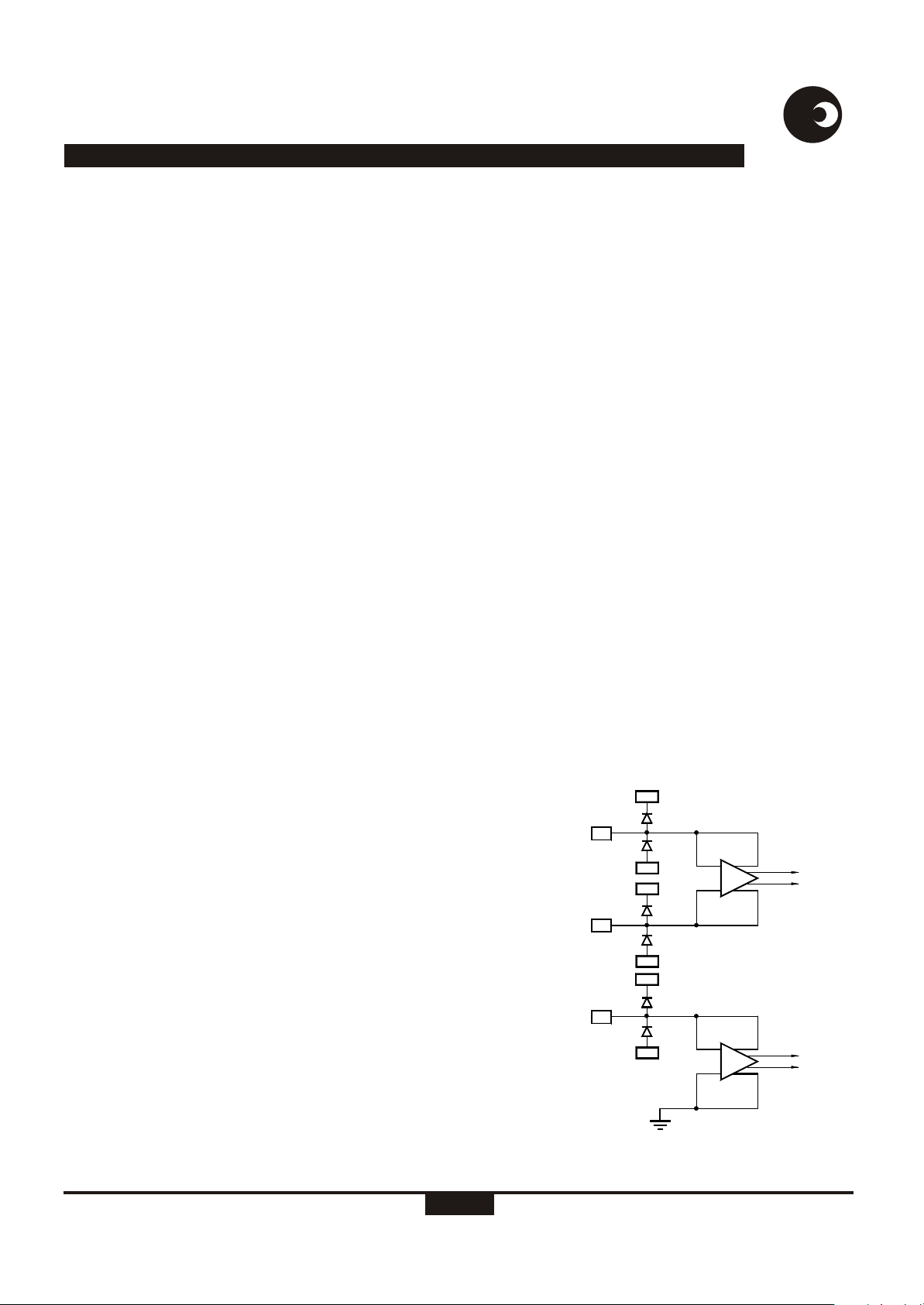
INPUT SIGNALS
ANALOG INPUT CONFIGURATION
The current and voltage sensor inputs are illustrated in figure 3.
These inputs are protected against electrostatic discharge
through clamping diodes, in conjunction with the amplifiers
input configuration. The feedback loops from the outputs of the
amplifiers A and A generate virtual shorts on the signal inputs.
Exact duplications of the input currents are generated for the
analog processing circuitry. The current and voltage sense
inputs are identical. Both inputs are differential current driven
up to ±25µA peak. One of the voltage sense amplifiers input
terminals is internally connected to GND. This configuration is
possible because the voltage sense input is much less
sensitive to externally induced parasitic signals compared to
the current sense inputs.
Current Sense Inputs (IIN1, IIP1, IIN2, IIP2, IIN3, IIP3)
The current sense inputs connects to a termination resistor
connected across the terminals of a current transformer. At
I V
V
DD
IIP
V
CURRENT
SENSOR
INPUTS
IIN
IVP
VOLTAGE
SENSOR
INPUT
DR-01288
SS
V
DD
V
SS
V
DD
V
SS
GND
A
I
A
V
Figure 3: Analog input internal configuration
http://www.sames.co.za
4/16
SA2005P
samessames
rated current the resistor values should be selected for input
currents of 16µA . Referring to figure 8, the resistors R1 and
RMS
R2 on current channel 1, resistors R3 and R4 on current
channel 2 and resistors R5 and R6 on current channel 3, define
the current level into the current sense inputs of the SA2005P.
The current sense inputs saturates at an input current of
±25µA peak. Resistors R29, R30 and R31 are used as current
transformer termination resistors. The voltage drop across the
termination resistors should be at least 20mV at rated
conditions. Values for the current sense inputs are calculated
as follows:
R1 = R2 = ( IL / 16µARMS ) x R29 / 2
R3 = R4 = ( IL / 16µARMS ) x R30 / 2
R5 = R6 = ( IL / 16µARMS ) x R31 / 2
Where:
I = Line current/CT-ratio
L
In case a current transformer is used for current sensing the
value of the termination resistors should be less than the
resistance of the CT's secondary winding.
Voltage Sense Inputs (IVN1, IVN2, IVN3)
The mains voltage are measured by means of a resistor divider
and the divided voltage are converted to a current. The current
into the voltage sense inputs (virtual ground) should be set to
14µARMS at rated voltage conditions. The individual mains
voltages are divided down to 14V per phase. The resistors
RMS
R12, R13 and R14 (figure 8) set the current for the voltage
sense inputs. The voltage sense inputs saturate at an input
current of ±25uA peak.
Voltage Reference Connection (VREF)
A bias resistor of 24k provides an optimum bias conditions on
chip. Calibration of the SA2005P is done by means of divider
ratios stored on an external EEPROM. This is described in the
Device Configuration section.
Serial Data (SDA)
The SDA pin connects directly to the SDA pin of an external
EEPROM. The pin is used to transfer data between the
EEPROM and the SA2005P. An external pull-up resistor in not
needed.
Serial Clock (SCL)
The SCL pin connects directly to the SCL of an external
EEPROM. The SCL output is used to strobe data at a rate of
50kHz out of the EEPROM. An external pull up resistor is not
needed. The SCL output uses a soft driver and may be
overdriven by the calibration equipment.
Reload (RLOAD)
A falling edge on the RLOAD pin will trigger a register update
from the external EEPROM. This feature may be used during
calibration to load updated register data in the SA2005P. For
normal operation of the SA2005P the RLOAD pin may be left
floating.
Test Inputs (TEST)
The TEST input is the manufacturers test pin and must be
connected to VSS in a metering application.
OUTPUT SIGNALS
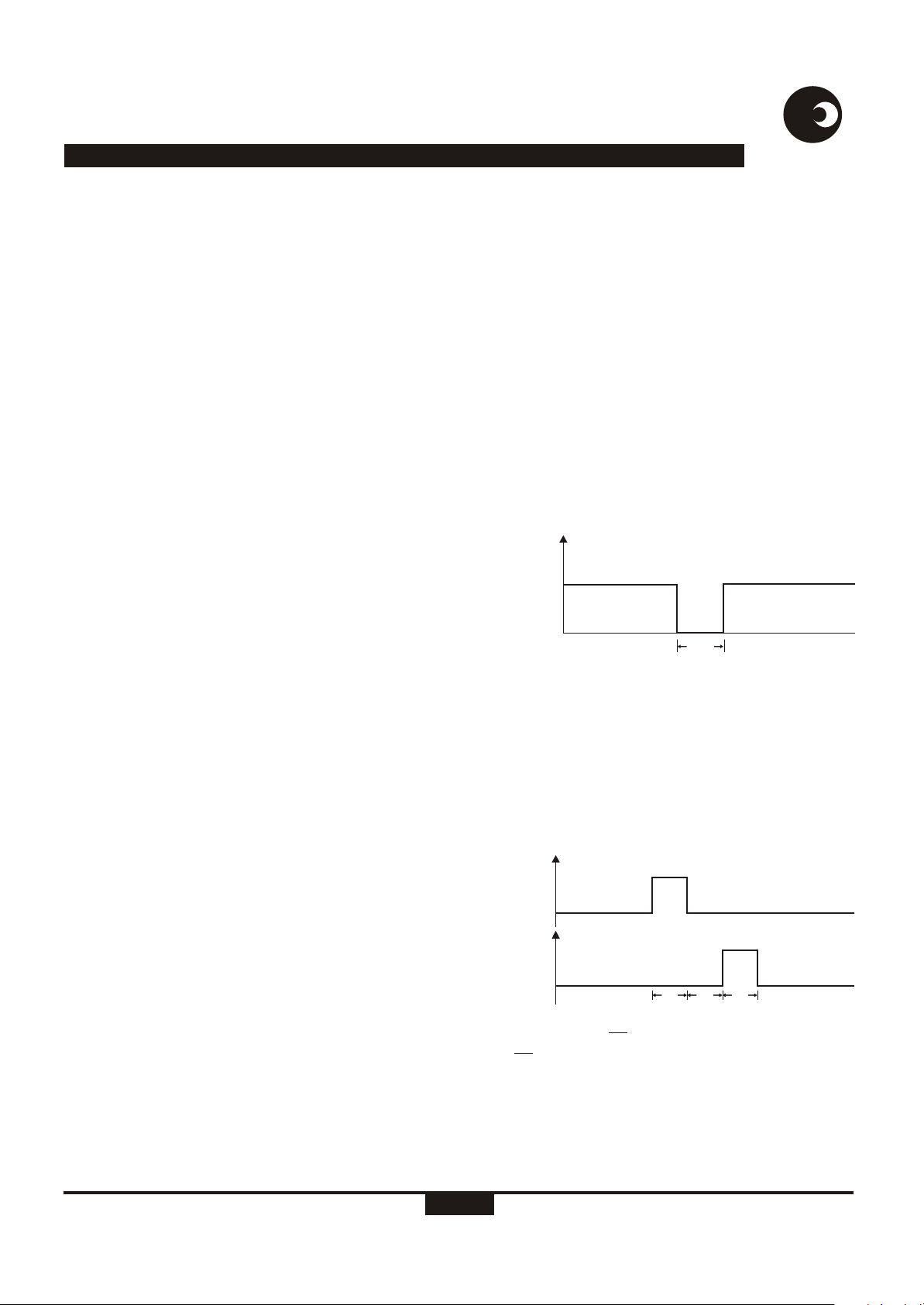
LED Output (LED)
Four options for the LED output pulse rate are available, 6400,
3200, 1600 pulses per kWh, and a pulse rate of 1252 pulses
per second at rated conditions. At 1252 pulses per second t LED
is 71µs, for the other options tLED is 10ms. The LED output is
active low as shown in figure 4.
VDD
LED
VSS
DR-01332
Figure 4: LED pulse output
Motor Output (MOP, MON)
The motor pulse width is programmable for 71ms, 142ms and
284ms. The MON pulse will follow the MOP pulse within the
selected pulse width time. This prevents the motor armature
being in the wrong position after a power failure. Both MOP
and MON outputs are active high. A MOP pulse followed by a
MON pulse represents one energy pulse. The motor drive
waveforms are shown in figure 5.
VDD
MOP
VSS
VDD
MON
VSS
DR-01559
Figure 5: Motor drive on MON and MOP pins of device
Multiplex Output (PH/ DIR)
The PH/DIR output enables either direction or voltage
information on the phase LED driver outputs (PH1, PH2 and
PH3). This multiplex output switches between logic 1 and 0 at
a frequency of approximately 280Hz. A logic 1 enables energy
direction information on the LED driver outputs and a logic 0
enables voltage information.
t
LED
t
m
t
t
m
m
http://www.sames.co.za
5/16
 Loading...