

INSTALLATION MANUAL
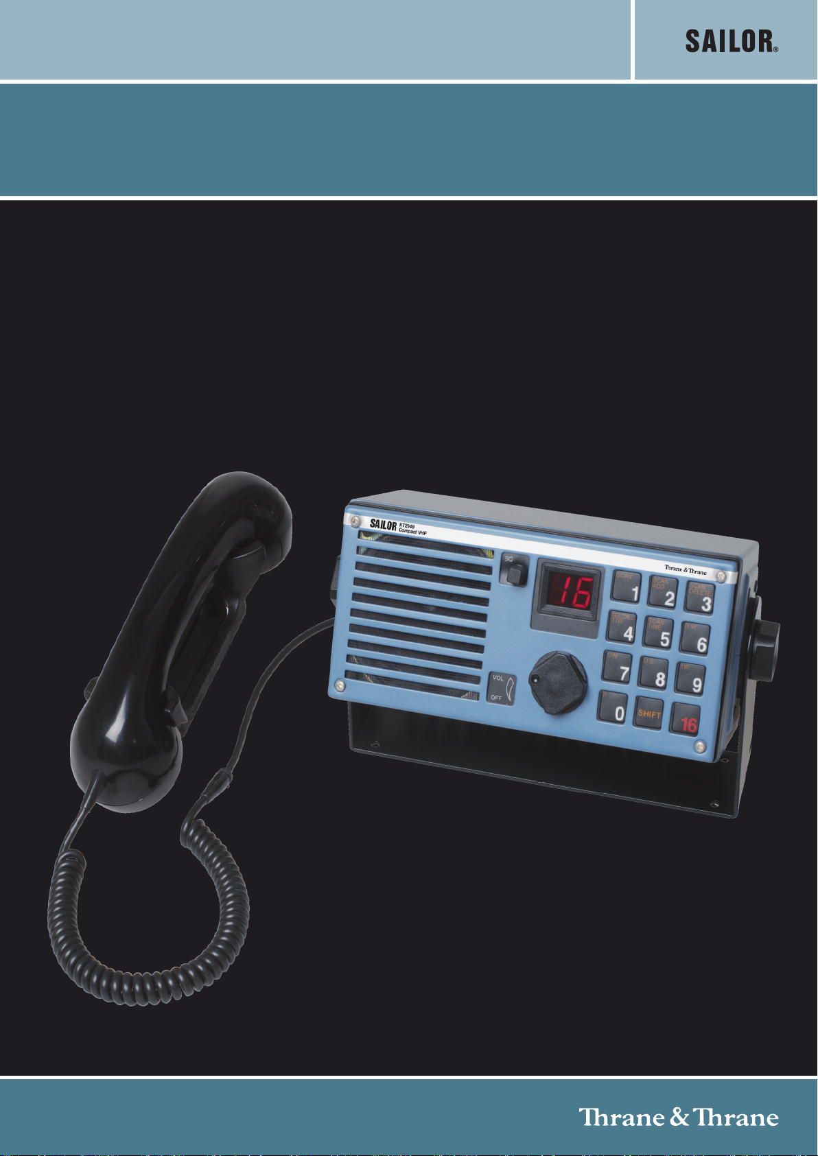
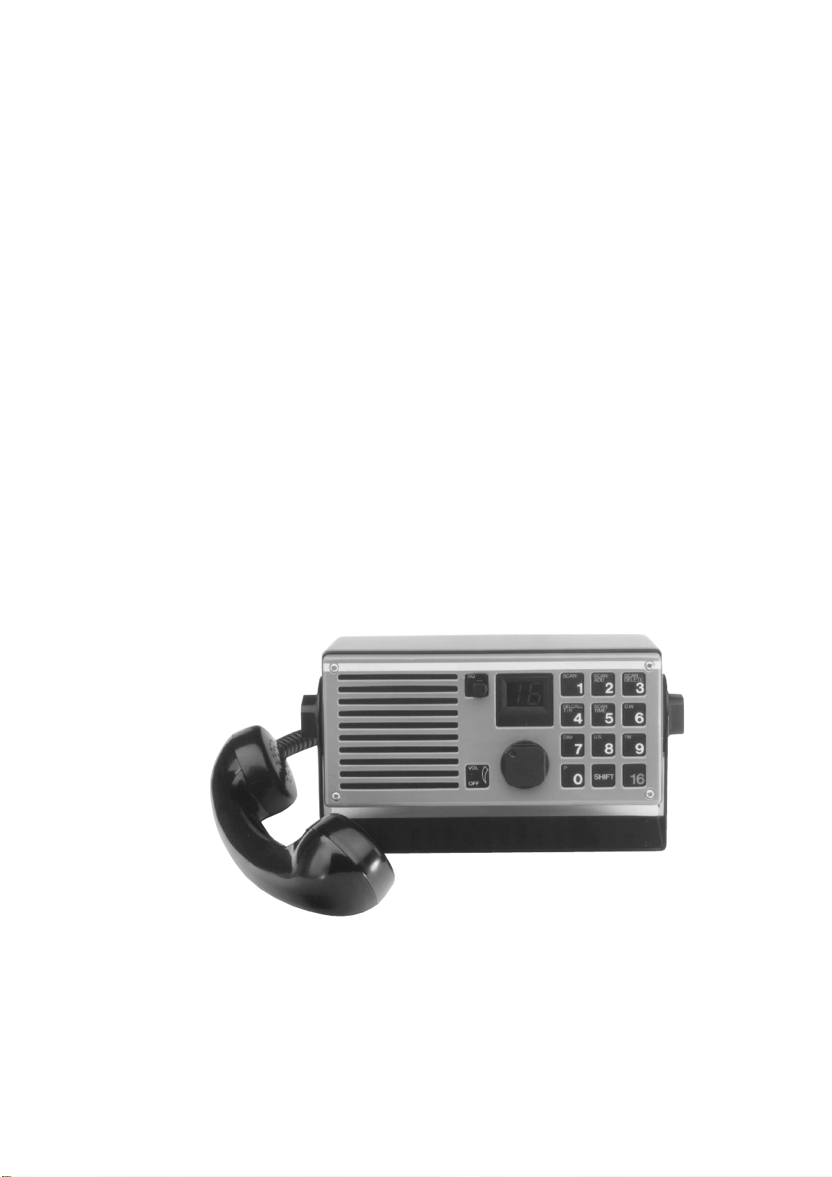
SAILOR RT2048 VHF

Disclaimer
Any responsibility or liability for loss or damage in connection with the use of this product and the accompanying documentation is disclaimed by Thrane & Thrane. The information in this manual is provided for information
purposes only, is subject to change without notice, may contain errors or inaccuracies, and represents no commitment whatsoever by Thrane & Thrane. This agreement is governed by the laws of Denmark.
Manuals issued by Thrane & Thrane are periodically revised and updated. Anyone relying on this information
should satisfy himself/herself as to the most current version. Providers with access to Thrane & Thrane’s Extranet may obtain current copies of manuals at: http://extranet.thrane.com.
Thrane & Thrane is not responsible for the content or accuracy of any translations or reproductions, in whole or
in part, of this manual from any other source.

RT2048
CONTENTS
1. INTRODUCTION 1-1
1.1. GENERAL DESCRIPTION 1-2
1.2. TECHNICAL DATA 1-3
1.3. CONTROLS 1-4
1.4. PRINCIPLE OF OPERATION 1-6
2. INSTALLATION 2.1
2.1. MOUNTING POSSIBILITIES 2-2
2.2. HANDSET 2-6
2.3. MICROTELEPHONE CONNECTOR 2-6
2.4. POWER SUPPLY 2-6
2.5. POWER CONNECTOR + EXT. LOUDSPEAKER 2-7
2.6. ANTENNAS 2-7
2.7. SPECIAL OPTIONS 2-7
2.8. REAR VIEW OF VHF RT2048 2-11
2.9. STANDARD FREQUENCY TABLE 2-12
3. SERVICE 3-1
3.1. MAINTENANCE 3-1
3.2. ALIGNMENT INSTRUCTIONS 3-1
3.3. PROPOSAL FOR NECESSARY MEASURING INSTRUMENTS 3-1
3.4. TEST PROBE 3-2
3.5. ADJUSTMENT PROCEDURE 3-2
3.6. TROUBLESHOOTING 3-3
3.7. REPLACEMENT OF COMPONENTS 3-4
3.8. REPLACEMENT OF MODULES 3-4
3.9. NECESSARY ADJUSTMENTS AFTER REPLACEMENT
OF MODULE 3-4
3.10. PIN CONFIGURATIONS 3-5
4. MODULE LOCATION 4-1
4.1. MECHANICAL DISASSEMBLING RT2048 4-2
5. CIRCUIT DESCRIPTION AND SCHEMATIC DIACRAMS 5-1
5.1. KEYBOARD UNIT (MODULE 1) 5-1
5.2. INTERFACE UNIT (MODULE 2) 5-3
5.3. SYNTHESIZER UNIT (MODULE 3) 5-6
5.4. Rx/Tx UNIT (MODULE 4) 5-10
5.5. SELCALL UNIT (MODULE 5) OPTIONAL 5-14
5.6. INTERCONNECTION CABLE DIAGRAM 5-16
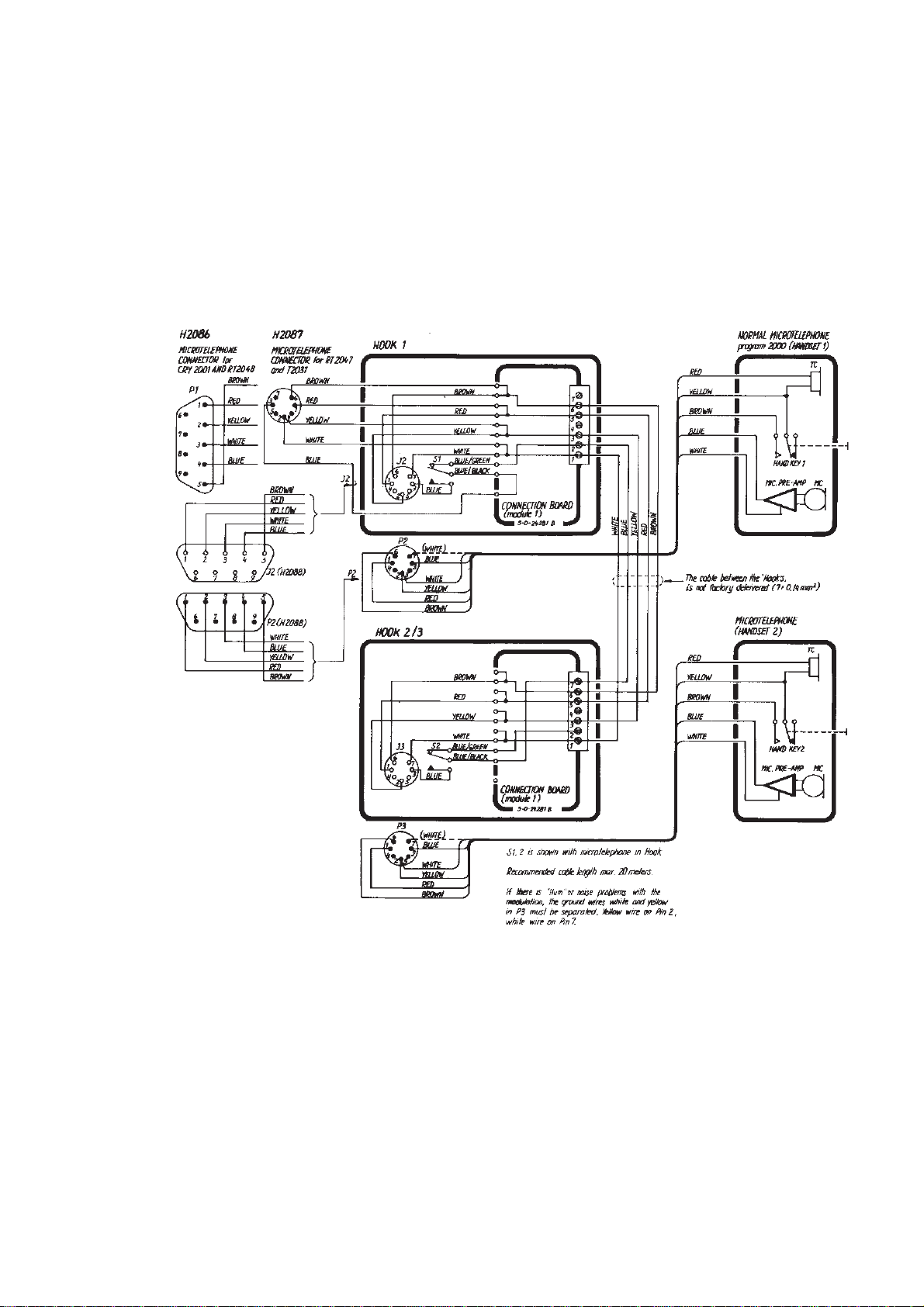
6. MICROTELEPHONE INSTALLATION 6-1
6.1. SPECIAL INSTALLATION WITH 2 MICROTELEPHONES 6-3
6.2. SPECIAL INSTALLATION WITH 3 MICROTELEPHONES 6-4
6.3. MECHANICAL DIMENSIONS FOR HANDSET 6-5
7. PARTS LIST 7-1
Appendix A - ATIS OPTION (OPTIONAL)
9403


RT2048
CONTENTS
1. INTRODUCTION 1-1
1.1. GENERAL DESCRIPTION 1-2
1.2. TECHNICAL DATA 1-3
1.3. CONTROLS 1-4
1.4. PRINCIPLE OF OPERATION 1-6
9403

RT2048
1. INTRODUCTION
The RT2048 VHF radiotelephone has been designed to comply with the increasing demands of a highly technological
product, which means high quality, small size, etc.
The RT2048 is furthermore designed to fit into the Compact 2000 module programme.
The RT2048 can either be installed and operated as an independent unit, or in combination with other elements of
the Compact 2000 programme. These include a Duplex VHF radiotelephone, a coast telephone station with a 400W
PEP SSB transmitter and an SSB receiver with built-in FM and AM bands, and a scrambler which ensures complete
communication secrecy.
The VHF RT2048 has, by means of the latest technology in casting technique, been constructed to withstand the
most extreme conditions experienced in small, semi-open boats. The printed circuits inside are designed with a high
degree of compactness and exceptional performance.
In the design of this VHF radiotelephone, S. P. Radio have taken into account all the circumstances it will be exposed
to in day-to-day operation. However, even a product of this high quality requires regular servicing and maintenance,
and we recommend a close observance of the directions contained in the instruction book.
S. P. Radio is one of Europe’s leading producers of maritime radio communication equipment - a position which has
been maintained by means of constant and extensive product development. We have a world-wide network of dealers
with general agencies in fifty countries. All our dealers are well-trained and able to service all S.P. Radio products
9403
Page 1-1

1 INTRODUCTION RT2048
1.1. GENERAL DESCRIPTION
VHF RT2048 is an all solid state constructed microcomputer controlled VHF radiotelephone, intended for ship/ship
and ship/shore communication.
VHF RT2048 can operate in both simplex and semi-duplex mode.
VHF RT2048 includes all 55 international and U.S. VHF marine channels, and is as standard prepared for up to 10
private channels, selected as simplex or semi-duplex channels in the frequency band 154.4 -
163.75 MHz.
VHF RT2048 is equipped with flexible scanning facilities or additional 30 private channels in the above mentioned
frequency band.
VHF RT2048 has built-in dual watch facility, which enables the operator to listen out on two channels simultaneously
(the selected channel and a programmable preference channel - normally channel 16).
VHF RT2048 is provided with a quick select channel, normally channel 16.
VHF RT2048 is provided with continuous turn-style operation of SQ and AF level for optimum resolution.
VHF RT2048 is provided with a push-button keyboard offering an attractive tactile feeling and a safe finger-guide in
the metal front. Besides, the keyboard is fitted with night-illumination of the lettering from behind.
VHF RT2048 has a high efficient LED read-out of channel number and other indications for optimum reading under
all conditions.
VHF RT2048 is a modern transceiver with an all synthesized frequency generation based on a single crystal.
VHF RT2048 has a built-in 12W AF power amplifier, which delivers 6W into the large built-in loudspeaker.
VHF RT2048 is for 12V DC supply. Voltage change-over from 24V to 12V is easily done by the power supply N420.
VHF RT2048 has an extremely low standby current consumption, typically below 100 mA.
VHF RT2048 is housed in a corrosion resistant metal cabinet with a green nylon finish.
VHF RT2048 can be delivered with a built-in selcall decoder, which will decode a selective call CA or all ships call
CQ
Page 1-2
9403

1 INTRODUCTION RT2048
1.2. TECHNICAL DATA
Fulfils the international CEPT regulations.
GENERAL
All international maritime VHF channels
Private channels: 10, may be extended to 40
Operation: Simplex and semi-duplex
Modulation: G3EJN (Phase)
Antenna impedance: 50 ohm
Frequency stability: +/- 10 ppm (Spec. vers. +/- 5 ppm)
Temperature range: -20oC to +55oC
Nominal power supply: 13.2V DC
Power supply variation: 12V DC -10% to +30%
(with data according to international standards)
Power consumption: Standby = 0.1 A
Transmit = 5 A
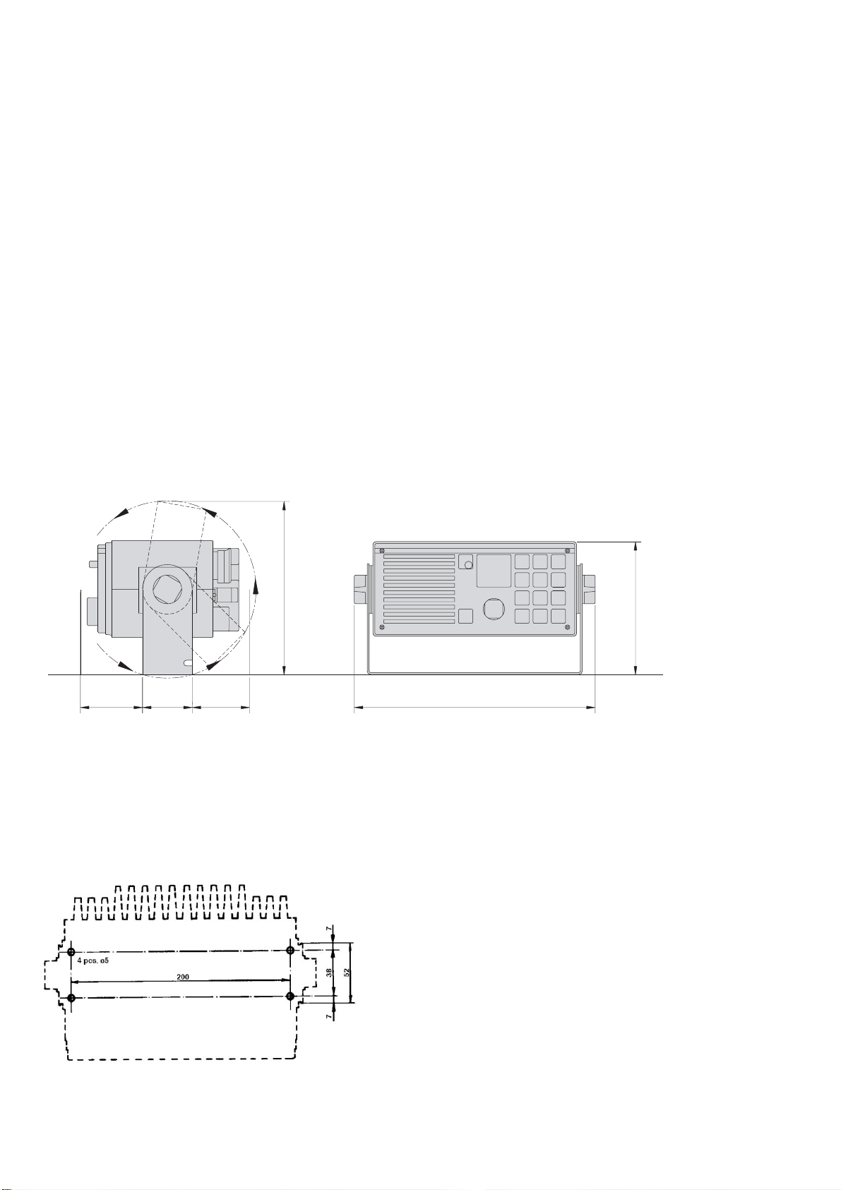
Dimensions: Height: 98 mm
Width: 225 mm
Depth: 160 mm
Weight: 3.1 kg
RECEIVER
Frequency range simplex: 154.40 - 159.15 MHz
Frequency semi-duplex: 159.00 - 163.75 MHz
Sensitivity: 0.25 uV P D a t 1 2 d B S I N AD
AF output power: 6 Watt/4 ohm
Telephone output: 0.5V RMS/200 ohm
Distortion: Less than 5%
Scanning facilities: Flexible scanning programme,
with possibility for all international
channels and 10 private channels.
Accessory: Selcall decoder according to
CCIR
TRANSMITTER
Frequency range normal: 154.40 - 159.15 MHz
Frequency range special: 159.00 - 163.75 MHz
RF output power: 25 Watt +0 to -0.5 dB
Reduced RF output: 0.5 to 1 Watt
Distortion: Less than 5%
9403
Page 1-3

1 INTRODUCTION RT2048
2
1.3. CONTROLS
9656
VOL
OFF
SQ
1W Tx
VOL
OFF
Indication of ON/OFF/VOL turn-style knob operation.
US
SCAN
1
SELCALL
T / R
4
DIM
7
P
0
ADD
2
SCAN
TIME
5
U.S.
8
SHIFT
SCANSCAN
DELETE
3
D.W.
6
1W
9
16
SQ
16
SCAN
1
SHIFT
SHIFT
SHIFT
Squelch sensitivity control knob with turn-style operation.
Quick selection of the call and distress channel 16.
Digits from 1 to 0
Activates the functions marked in orange on the keyboard.
Whenever the keyboard is in “shift-mode” it will be
indicated by “cornerbars” in the display
SCAN
Selects scanning programme.
1
SCAN
ADD
Adds a channel to the scanning table.
2
1W Tx US
SHIFT
Page 1-4
SCAN
DELETE
3
Deletes a channel from the scanning table.
9403
1 INTRODUCTION RT2048
SHIFT
SHIFT
SHIFT
SHIFT
SHIFT
SHIFT
SCAN
TIME
5
D.W.
6
1W
9
U.S.
8
DIM
7
SELCALL
T / R
4
Selects the scan time from 1 to 99 seconds.
The time chosen is the listening time on one of the secondary channels receiving
a signal.
Selects the dual watch facility.
Selects 1W reduced power output.
Selects the VHF channels used in the USA.
The intensity of the LED-indicators can be controlled in four steps.
The keyboard illumination is switched on and off.
Tests the selcall decoder and resets the selcall decoder after a call.
P
SHIFT
Selects the standard private channels.
0
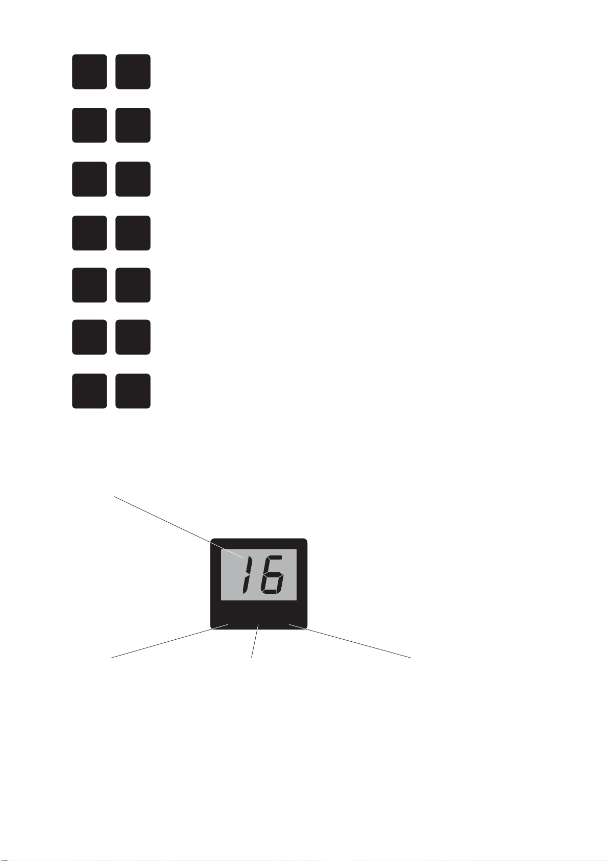
READ-OUT
Channel Read-Out All international maritime channels are shown by the two digits,
when the channel has been keyed in.
Selection of a standard private channel will be indicated with a P-.
1W Tx US
Reduced Power
In harbour areas or in the close
vicinity of another vessel,
transmissions should be with
reduced power.
When the display shows 1W,
the transmitter output power is
reduced from 25W to 1W
Where two stations are close
together, this reduction can
improve communication quality.
Transmitting
Whenever the handset switch
is depressed, and the transmitter
output power level has reached
an appropriate level, the "TX"
will appear.
US-Channels
In the USA a number of the
international duplex channels
are used as simplex channels.
Ships sailing in American waters
must therefore be able to select
these channels as simplex channels.
The appearance of "US" on the
display indicates that this mode of
operation is in use.
9403
29655
Page 1-5

1 INTRODUCTION RT2048
1.4. PRINCIPLE OF OPERATION
FREQUENCY GENERATION
All the internal frequencies are referenced to a crystal oscillator, running on 14.85 MHz.
The 14.85 MHz is divided by 4 in the REFERENCE DIVIDER, to generate a 3.7125 MHz signal, which is the input
to the PLL-reference divider and clock-signal for the microcomputer.
The local oscillator signal for the first mixer in the receiver and the transmit signal are generated in a phase-locked
loop (PLL). To generate the needed frequencies, which are specified as follows:
139.1 MHZ
159.0 MHz
< fLO1 < 148.45 MHz; 154.5 MHz < fTX NORMAL < 159.15 MHz
< fTX SPECIAL << 163.75 MHz
a bandshift is performed in the VCO.
The loop reference frequency - and so the resolution - is 12.5 kHz, derived by dividing the reference divider output
with 297.
The VCO output frequency is divided down to 12.5 kHz after the dual-modulus principle with a PRESCALER dividing
with 32/33.
The phase detector output controls the CHARGE PUMPE feeding the loop filter integrator.
If there is a difference in phase/frequency between the inputs to the phase detector. An error current from the charge
pumpe will be integrated in the loop filter, producing the needed voltage for the VCO.
RECEIVER
The antenna signal is fed to the RX AMPLIFIER through the RX/TX relay.
The bandpass filters around the RX amplifier are tuned by means of capacitor diodes, which are controlled by a DCvoltage derived from the VCO control voltage in the PLL.
The received signal is converted to the first intermediate frequency on 15.3 MHz in the FIRST MIXER, using the VCO
signal from the RX BUFFER AMPLIFIER as local oscillator signal.
The signal is filtered and amplified before down-conversion to 450 kHz in the SECOND MIXER. The crystal oscillator
signal is used as local oscillator signal.
After filtering in the SECOND IF FILTER, the signal is amplified and detected.
The AF signal is passed through a mute switch before undergoing appropriate amplification and filtering to get the
right frequency response.
Besides, the detected output is filtered in the SQUELCH FILTER before it is amplified, detected, and compared with
a reference level to get a logical level for the microcomputer, which controls the mute circuit.
The telephone amplifier and the AF power amplifier produce the wanted output levels for the earpiece and the
loudspeaker.
TRANSMITTER
The signal from the microphone is passed through a PRE-EMPHASIS network before appropriate amplification and
compression in the AF AMPLIFIER COMPRESSOR.
This signal is filtered before it is fed to the VCO, where the modulation of the transmitter signal takes place.
As the VCO oscillates direct on the transmitting frequency in TX-mode, the signal only has to be amplified. This is
done in the TX BUFFER AMPLIFIER and the TX POWER AMPLIFIER.
The power supply for the TX power amplifier is regulated by a feed-back loop via the POWER SENSE circuit to
maintain constant output power level. Switching between full and reduced output power level is made by means of
the PA-REGULATOR.
To reduce the level of harmonic components in the output signal it is passed through a HARMONIC FILTER before
it is led to the antenna via the RX-TX-RELAY.
MICROCOMPUTER
The microcomputer on the interface unit is taking care of various functions, among these the user interface, which
means reading of the keyboard and readout to the LED-display via the DISPLAY-LATCHES.
Moreover the computer calculates the appropriate division figures for the PLL, controls the transmitter power level,
the AF mute circuits, and reads and writes to the EEPROM’s.
When a selcall unit is installed, the microcomputer also controls the selcall switch capacitor filter.
The serial interface is only for factory production use.
Page 1-6
9403

1 INTRODUCTION RT2048
BLOCK DIAGRAM
9403
Page 1-7


RT2048
CONTENTS
2. INSTALLATION 2.1
2.1. MOUNTING POSSIBILITIES 2-2
2.2. HANDSET 2-6
2.3. MICROTELEPHONE CONNECTOR 2-6
2.4. POWER SUPPLY 2-6
2.5. POWER CONNECTOR + EXT. LOUDSPEAKER 2-7
2.6. ANTENNAS 2-7
2.7. SPECIAL OPTIONS 2-7
2.8. REAR VIEW OF VHF RT2048 2-11
2.9. STANDARD FREQUENCY TABLE 2-12
9403


2. INSTALLATION
Before installation of a SAILOR VHF RT2048 the following points must be observed:
1. Which facilities have to be enabled?
Selcall, private channels, US-mode, dual watch, scanning facilities, etc. The procedure how to enable the
facilities is described in the manual: INSTRUCTIONS FOR IDENTITY AND SERVICE PROGRAMMING OF
SAILOR VHF RT2048.
This manual will only be delivered to dealers and general agents, where it must be at the disposal of trained
service people in the service workshop.
2. In what way the VHF RT2048 has to be installed?
In the section MOUNTING POSSIBILITIES, the installation of VHF RT2048 is described either as an
independent unit or in combination with the other elements of the Compact 2000 programme.
3. Handset.
Installation of handset, see the section HANDSET.
4. External loudspeaker.
An external loudspeaker 4-8 ohm/6W can be connected to the power connector J1, pin 1 and 6, see the
section POWER CONNECTOR + EXT. LOUDSPEAKER.
RT2048
5. Special options:
Remote alarm for selcall, AF to information decoder, AUX I and AUX II information, etc. are available, see
the section SPECIAL OPTIONS
9346
Page 2-1
2 INSTALLATION RT2048
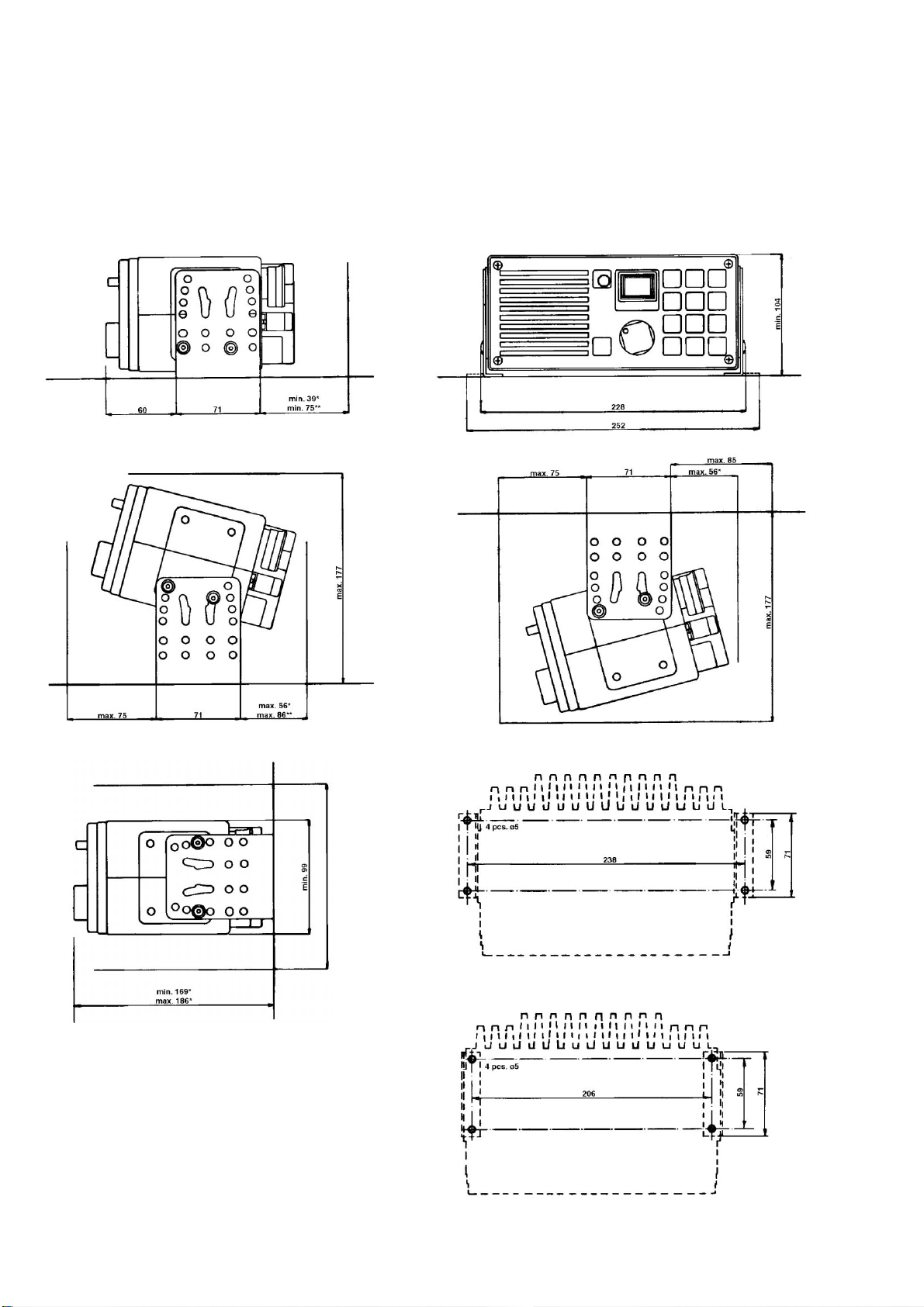
2.1. MOUNTING POSSIBILITIES
The VHF RT2048 cabinet is designed in a module called a mini 1/4 box. For this module we can supply a wide variety
of installation brackets etc. which will be described below. We have made a drawing including dimensions and
drilling plan for each type and we kindly ask you to look at the drawing for the type in question.
H2077 MULTI-PURPOSE MOUNTING BRACKET
This mounting bracket is as standard delivered together with RT2048. It permits a wide variety of installation
possibilities such as tabletop, bulkhead or deckhead. It is easy to remove the set by unscrewing the two buttons
of H2077.
H2077
o
290
182
25572
25572 25571
*max. 60
52max. 65
**max. 96 252
139
25668
Page 2-2
Weight:
Mounting kit H2077: 0.4 kg
VHF RT2048: 3.2 kg
9346

2 INSTALLATION RT2048
H2067 MOUNTING BRACKET FOR TABLETOP, BULKEHAD OR DECKHEAD MOUNTING FOR MINI 1/4 BOX
This mounting bracket is used when RT2048 is to be mounted next to other SAILOR units in the Compact 2000
programme mounted in H2055 mounting brackets. For example when installing the RT2048 next to the scrambler
CRY2001 it is possible to tilt both units in the same angle.
H2067
25574 25573
25575
25659A
Weight:
Mounting kit H2067: 0.5 kg
VHF RT2048: 3.2 kg
9346
Page 2-3
2 INSTALLATION RT2048
H2057 ANGLE HINGES FOR TABLETOP, BULKHEAD OR DECKHEAD MOUNTING FOR MINI 1/4 BOX
H2057 is designed for stationary installation. It offers a lot of mounting possibilities using the different holes in the
angle hinges when tilting the VHF.
H2057
25534 25530
25531A 25531
25669
25533
* Dimensions when using a right-angled VHF plug.
** Dimensions when using a standard VHF plug.
Weight: Mounting kit H2057: 0.4 kg
VHF RT2048: 3.2 kg
Page 2-4
25670
9346
2 INSTALLATION RT2048
H2063 CONSOLE MOUNTING KIT FOR 1/4 BOX
This mounting kit is used for console flush mounting of 1/4 box and mini 1/4 box.
Free distance must be kept to allow free air circulation, ambient temperature max. 40
o
C.
H2063
25663
Weight:
Mounting kit H2063: 1.0 kg
VHF RT2048: 3.2 kg
24703
9346
25657
Page 2-5

2 INSTALLATION RT2048
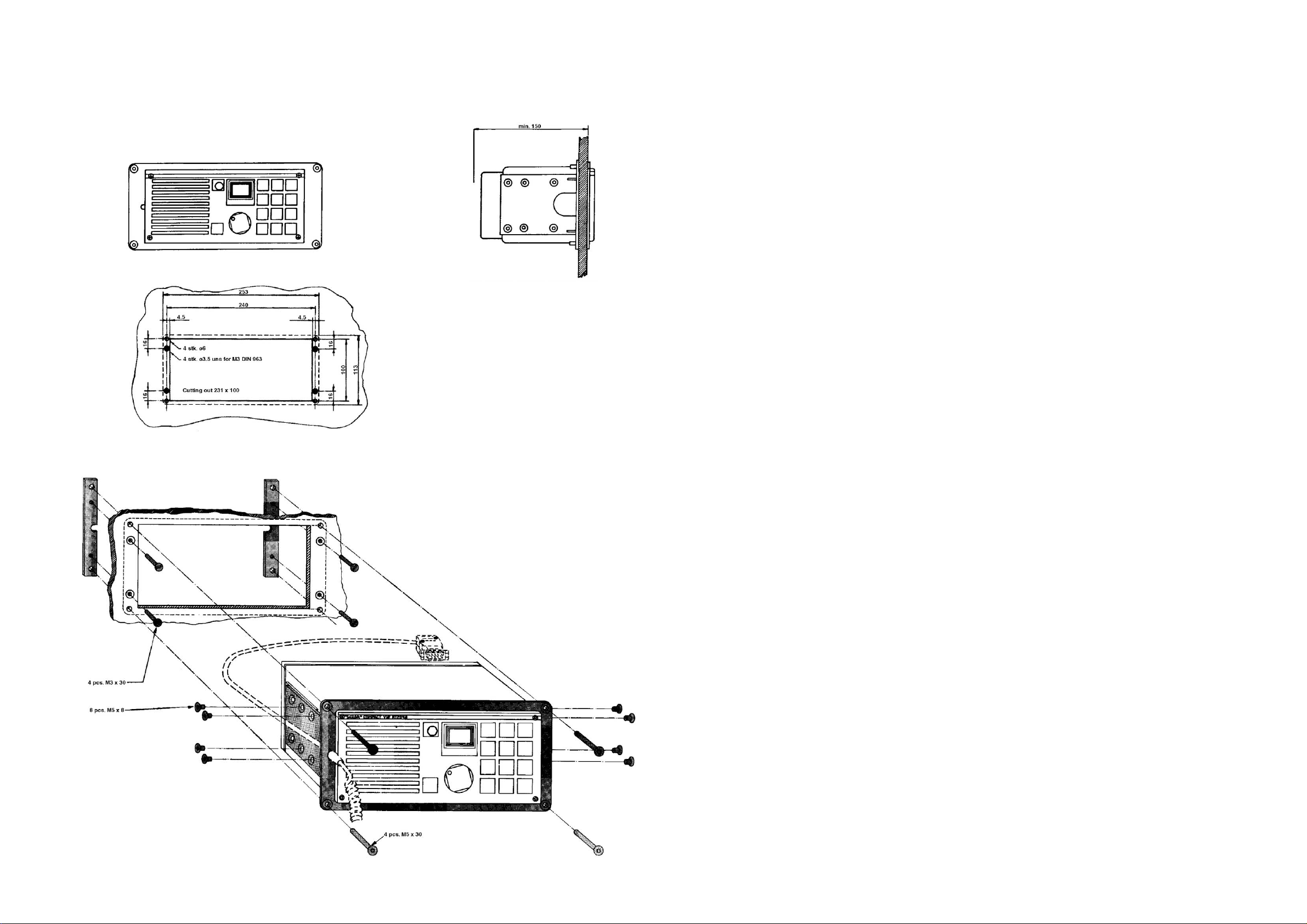
2.2. HANDSET
The handset can be placed anywhere near the VHF set. The cable is five-cored and connected to the rear
of the VHF through a 9-pole Sub-D connector.
Installation of the cable, see the drawings of the mounting brackets. The cable grommet must be placed
in the most convenient groove in the mounting bracket.
If more than one handset is needed, please see the section SPECIAL INSTALLATION WITH 2 OR 3
MICROTELEPHONES.
2.3. MICROTELEPHONE CONNECTOR
Pin No. 1 Telephone
Pin No. 2 GND
Pin No. 3 GND
Pin No. 4 Mic
Pin No. 5 Key
Pin No. 6 Spare
Pin No. 7 Distress CRY*
Pin No. 8 “Serial input”
25666 Pin No. 9 +13V internal
25664
* only active when option board pcb is installed.
2.4. POWER SUPPLY
The standard power supply for RT2048 is 12V DC. For 24V DC supply an external power supply N420
(a 24V DC to 13.2V DC serial regulator) can be used.
For 110V AC, 127V AC, 220V AC, or 237V AC operation an external power supply N163S must be used
together with N420.
Page 2-6
25665
9346

2 INSTALLATION RT2048
2.5. POWER CONNECTOR + EXT. LOUDSPEAKER
VIEW FROM MOUNTING SIDE
Pin No. 1 Ext. loudspeaker
Pin No. 2 Ext. mute*
Pin No. 3 +12V power supply
Pin No. 4 on/off for 24V supply
Pin No. 5 -12V power supply
Pin No. 6 Ext. loudspeaker
24914
* only active when option board pcb is installed.
If necessary a 4-8 ohm/6W external loudspeaker can be connected to pin No. 1 and pin No. 6 in the power connector
J01 (observe that there is DC voltage on both wires).
External loudspeakers SAILOR H2054 and H2074 are available.
2.6. ANTENNAS
All common 50 ohm antennas, which cover the used frequency range with a reasonable standing wave ratio,
maximum 1.5, are available.
The antenna is connected to the set by means of a 50 ohm coaxial cable with low loss, e.g. RG213U. At the cable
end a PL259 plug is mounted.
The antenna must be placed as high and clear as possible. The horizontal distance to metal parts must be at least
one metre.
S. P. Radio has an antenna of the necessary specifications available. The mentioned antenna is characterized by
small external dimensions. For further particulars see special brochure VHF AERIALS.
2.7. SPECIAL OPTIONS
With a small modification in RT2048 the following options are available:
1. K-switch function (used on river boats in Germany). Can be enabled by means
of the identity programming. US-button is changed to K-switch.
2. With DISTRESS OPTION installed
S.P. No. 625661
a. Distress output to CRY2001/2002.
3. With SELCALL OPTION installed
S.P. No. 625660
a. SELCALL RELAY, when the selcall has accepted a CQ or an individual call signal, the selcall
relay will turn on and short circuit two wires, which can be used for remote alarm.
Max. contact load: 100V AC/24V DC - 2A.
9346
b. AF TO INFORMATION DECODER, the circuit giving AF signals to the information decoder
is turned on when the set has accepted a CQ or an individual call signal. The circuit is turned
on/off by the microprocessor.
Page 2-7

2 INSTALLATION RT2048
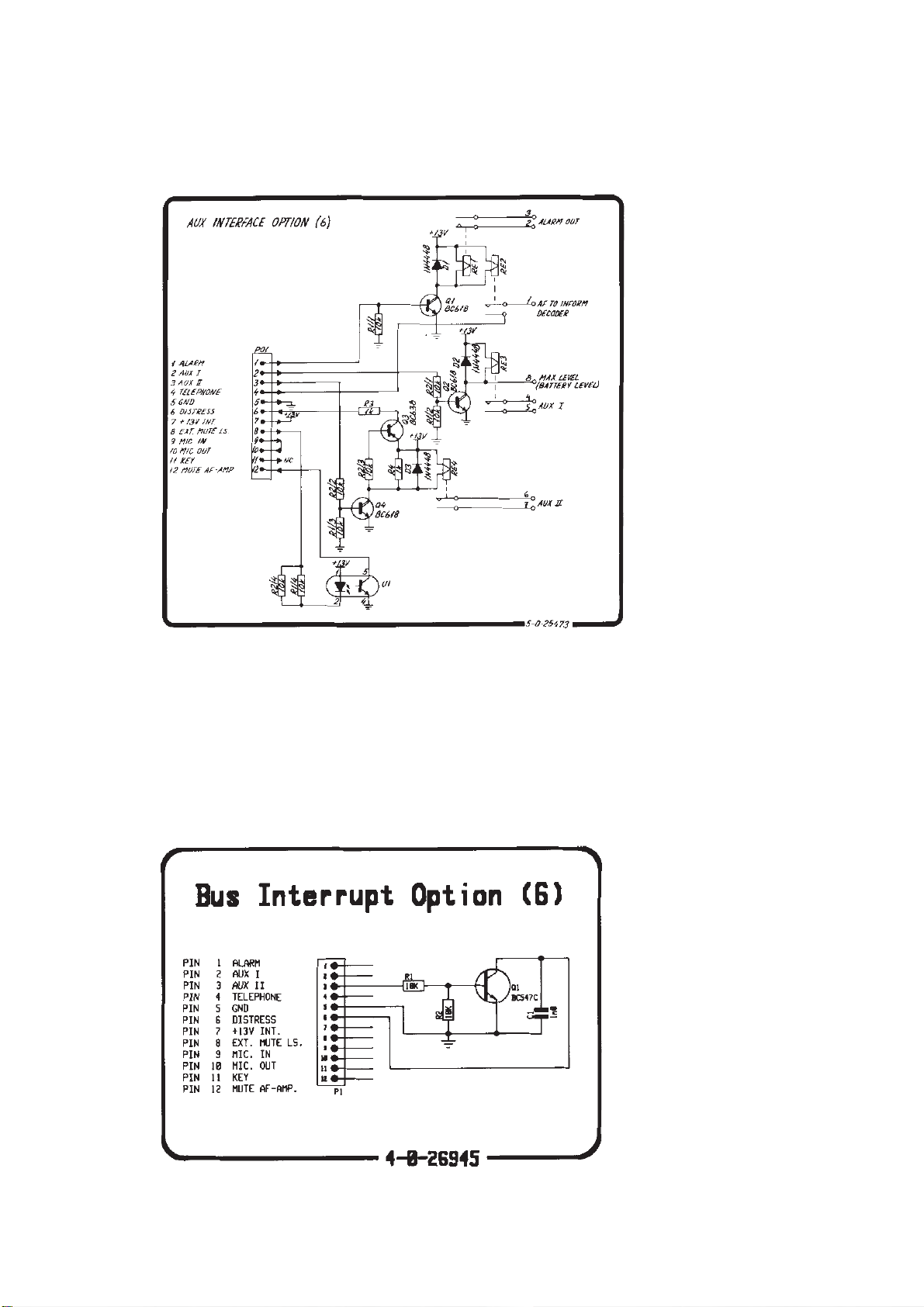
4. With AUX INTERFACE OPTION installed
S.P. No. 625473
(AUX1, AUX2 and MUTE functions) (Distress and Selcall functions are also mounted).
a. AUX2, when information on certain channels is wanted, i.e. controlling a watch keeping
receiver, the AUX2 information can be used, a relay is controlled from the microprocessor.
Max. contact load: 100V AC/24V DC - 2A.
b. AUX1, when function code in Prom 1 is enabled, AUX1 is free programmable on all
international channels (“0” or “1”).
Standard programming on international channels is “0”.
Max. contact load: 100V AC/24V DC-2A.
c. MUTE, makes it possible to mute AF power amplifier from external equipment.
Activated by a make function between pin 5 and pin 8 in P1 on option board.
5. With BUS INTERRUPT OPTION installed
S.P. No. 626945
This module is used for interface to VHF DSC RM2042.
6. With ATIS OPTION installed
S.P. No. 728665
The module 628652 is used for interface to ATIS module 626707, which is mounted on this PCB.
For circuit description and programming of ATIS option please refer to Appendix A - ATIS OPTION
25662A
COMPONENT LOCATION FOR SPECIAL OPTIONS MODULES
VALID FOR 625661 / 625660 / 625473
Seen from component side Seen from component side
with upper side tracks. with lower side tracks.
PCB rev. 25473
Page 2-8
9346

2 INSTALLATION RT2048
COMPONENT LOCATION FOR 626945
Seen from soldering side Seen from soldering side
with soldering side tracks. with component side tracks.
PCB rev. 26945
DIAGRAMMES FOR SPECIAL OPTIONS
625660
9346
625661
Page 2-9
2 INSTALLATION RT2048
625473
Page 2-10
626945
9346
2 INSTALLATION RT2048
2 INSTALLATION RT2048
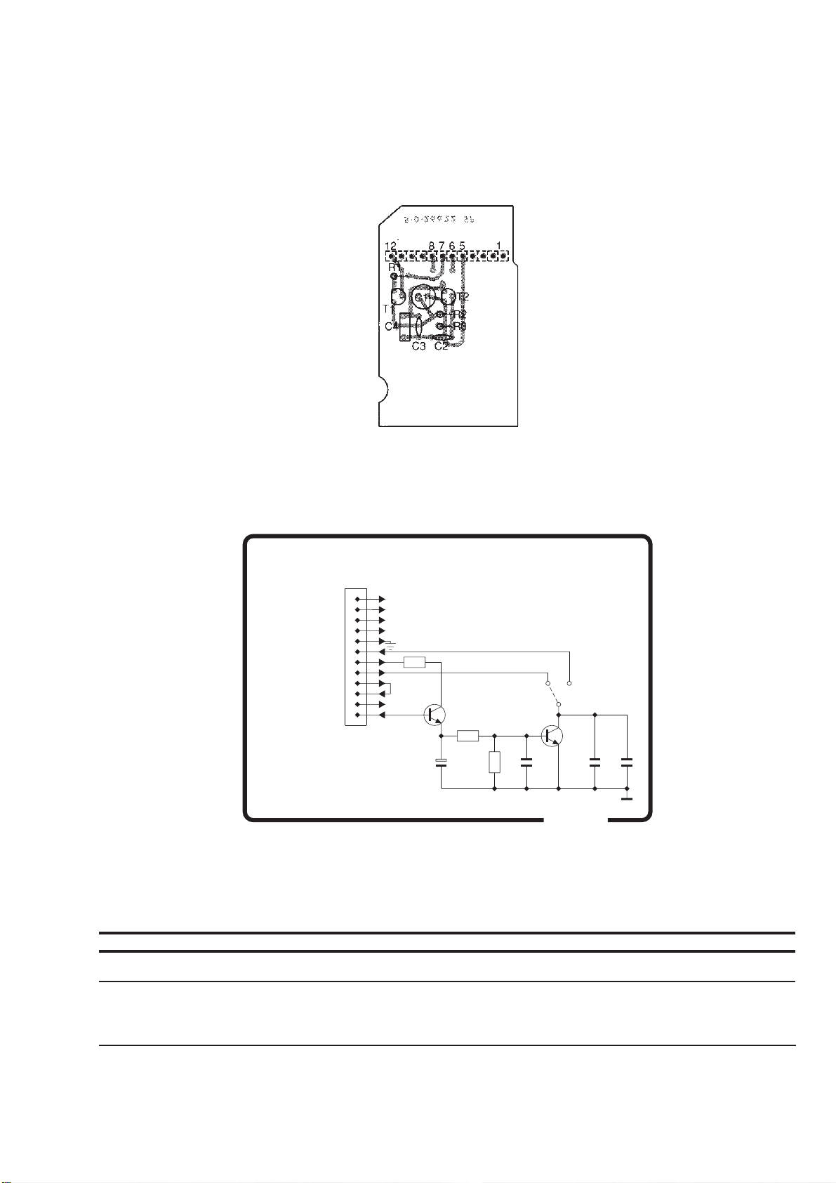
DELAYED KEY OPTION
To make a repeater station on a duplex channel, you need two pcs. of RT2048, one for receiving on Lo band, one
for transmitting on Hi band. To get this function, the function code has to be reprogrammed for the specified channel
in both sets. The modulation signal is taken on the earpiece from the receiver unit and led to the microphone input
of the transmitter unit. No attenuation required. The key for the transmitter unit is taken from the special option
board, Delay Key Option, to get the transmitter unit keyed approx. 10 seconds after last received signal.
Seen from component side with upper side tracks.
626622
1 ALARM
2 AUX I
3 AUX II
4 TELEPHONE
5 GND
6 DISTRESS
7 +13V INT.
8 EXT. MUTE LS.
9 MIC. IN
10 MIC. OUT
11 KEY
12 MUTE AF-AMP
10
11
12
DELAYED KEY OPTION (6)
P01
1
2
3
4
5
6
7
8
9
NC
470
R1
T1
BC548
R2
150
10uF
1M
R3C1C2
470p
4-0-26622
T2
BC548
1nC3C4
100n
DELAYED KEY OPTION MODULE (6) RT2048 ECI A/S 5-0-26622/2-0-25473A 626622
POSITION DESCRIPTION MANUFACTOR TYPE PART NO.
C1-6 CAPACITOR ELECTROLYTIC 10uF 20% 25VDC ELNA RBL-25-V-100-M-V2Z-T58 14.661
C2-6 CAPACITOR CERAMIC 470pF 10% 500VDC KCK RT-HM60 SK YB 471 K 16.095
C3-6 CAPACITOR CERAMIC 1nF 10% 50VDC CL2 KCK RT-SK-HE50 SJYB 102 K 16.160
C4-6 CAPACITOR MKT 0.1uF 10% 63VDC PHILIPS 2222 370 78104 11.136
J1-6 PLUG 1/10" SIL 12 POLES EURO DIP SL 12 O Z 78.328
R1-6 RESISTOR MF 470 OHM 5% 0.33W PHILIPS 2322 187 7347 02.464
R2-6 RESISTOR MF 150k OHM 5% 0.33W PHILIPS 2322 187 73154 02.524
R3-6 RESISTOR MF 1M OHM 5% 0.33W PHILIPS 2322 187 73105 02.544
T1-6 TRANSISTOR AF BC548 NPN TO-92 PHILIPS BC548 (-A/-B/-C) 28.070
T2-6 TRANSISTOR AF BC548 NPN TO-92 PHILIPS BC548 (-A/-B/-C) 28.070
9520
Page 2-10a

2 INSTALLATION RT2048
2.8. REAR VIEW OF VHF RT2048
25567
Page 2-11
9350

2 INSTALLATION RT2048
2.9. STANDARD FREQUENCY TABLE
RECEIVING FREQUENCY (MHz)TRANSMITTING
CHANNEL
01 156.050 156.050 160.650
02 156.100 160.700
03 156.150 160.750
04 156.200 160.800
05 156.250 156.250 160.850
06 156.300 156.300
07 156.350 156.350 160.950
08 156.400 156.400
09 156.450 156.450
10 156.500 156.500
11 156.550 156.550
12 156.600 156.600
13 156.650 156.650
14 156.700 156.700
15 156.750 156.750
16 156.800 156.800
17 156.850 156.850
18 156.900 156.900 161.500
19 156.950 156.950 161.550
20 157.000 161.600
21 157.050 157.050 161.650
22 157.100 157.100 161.700
23 157.150 157.150 161.750
24 157.200 161.800
25 157.250 161.850
26 157.300 161.900
27 157.350 161.950
28 157.400 162.000
60 156.025 160.625
61 156.075 160.675
62 156.125 160.725
63 156.175 156.175 160.775
64 156.225 160.825
65 156.275 156.275 160.875
66 156.325 156.325 160.925
67 156.375 156.375
68 156.425 156.425
69 156.475 156.475
70 156.525 156.525
71 156.575 156.575
72 156.625 156.625
73 156.675 156.675
74 156.725 156.725
75 156.775 156.775
76 156.825 156.825
77 156.875 156.875
78 156.925 156.925 161.525
79 156.975 156.975 161.575
80 157.025 157.025 161.625
81 157.075 157.075 161.675
82 157.125 157.125 161.725
83 157.175 157.175 161.775
84 157.225 161.825
85 157.275 161.875
86 157.325 161.925
87 157.375 157.375
88 157.425 157.425 157.425
WX1 Inhibit 162.550
WX2 Inhibit 162.400
WX3 Inhibit 162.475
WX4 Inhibit 161.650
FREQUENCY
(MHz)
US-MODE
(A.-CHANNELS)
INT'L MODE
(INT.-CHANNELS)
0549
Page 2-12


RT2048
CONTENTS
3. SERVICE 3-1
3.1. MAINTENANCE 3-1
3.2. ALIGNMENT INSTRUCTIONS 3-1
3.3. PROPOSAL FOR NECESSARY MEASURING INSTRUMENTS 3-1
3.4. TEST PROBE 3-2
3.5. ADJUSTMENT PROCEDURE 3-2
3.6. TROUBLESHOOTING 3-3
3.7. REPLACEMENT OF COMPONENTS 3-4
3.8. REPLACEMENT OF MODULES 3-4
3.9. NECESSARY ADJUSTMENTS AFTER REPLACEMENT
OF MODULE 3-4
3.10. PIN CONFIGURATIONS 3-5
9350


RT2048
3. SERVICE
3.1. MAINTENANCE
PREVENTIVE MAINTENANCE
If SAILOR RT2048 has been installed in a proper way the maintenance can be reduced to an overhaul at each visit
of the service staff. Then inspect the set, the antenna, cables, and plugs for mechanical damages, salt deposits,
corrosion, and any foreign material. Owing to its traditional structure, the SAILOR RT2048 has a long lifetime, but
it must always be carefully checked at intervals not exceeding 12 months - dependent on the conditions under which
the set is working. The set must be brought to the service workshop to be tested.
Along with each set a TEST-SHEET is delivered in which all the measurements, made in the test department of
the factory, are listed. If the control measurings made in the service workshop should not show the same values
as those listed in the test-sheet, the set must be adjusted as specified in the ADJUSTMENT PROCEDURE.
3.2. ALIGNMENT INSTRUCTIONS
INTRODUCTION
The measuring values indicated in paragraph 2 of CIRCUIT DESCRIPTION AND SCHEMATIC DIAGRAMS are
typical values and as indicated it will be necessary to use instruments in absolute conformity with the below list:
3.3. PROPOSAL FOR NECESSARY MEASURING INSTRUMENTS
VHF Signal Generator type TF2015 MARCONI
FM Modulation Meter type TF2303 MARCONI
Distortion Analyzer type TF2337A MARCONI
AF Voltmeter type VT-121 TRIO
Tone Generator type PM5107 PHILIPS
Electronic Multimeter type PM2505 PHILIPS
RF Directional Wattmeter Model 43 BIRD SOW
Load with 30 dB Attenuator type 8321 BIRD
Frequency Counter:
Frequency range >175 Mhz
Sensitivity <100 mv
Impedance >1 Mohm and 50 ohm
Accuracy <1 - 10
We can also recommend one of the new communication test sets introduced by several instruments manufacturers.
From S. P. Radio this high quality product will be tested and adjusted by means of a CMT communication tester
from Rohde and Schwarz.
-6
Page 3-1
3 SERVICE RT2048
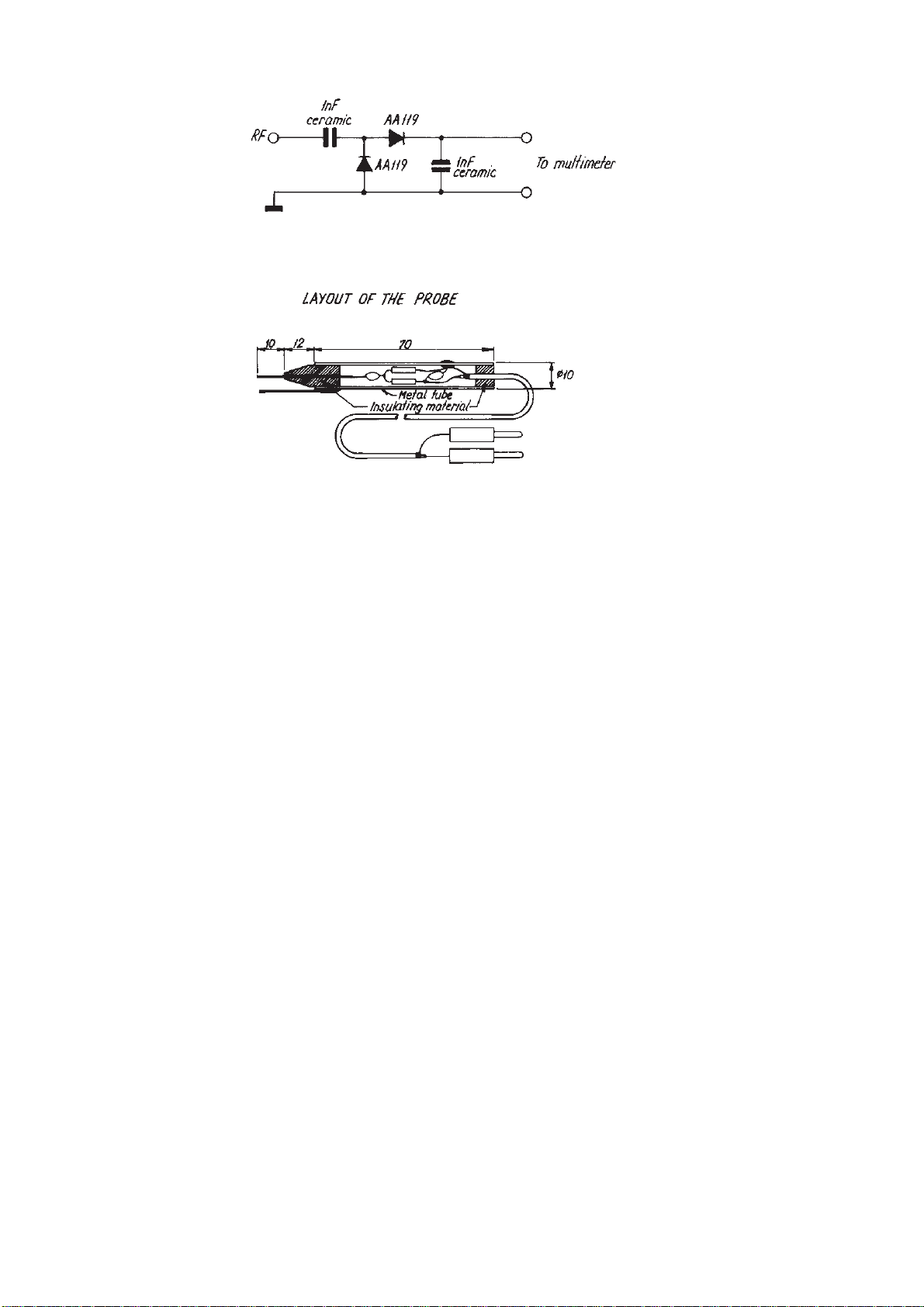
3.4. TEST PROBE
All measurings made by means of a test probe will be relative measurements. For quantitative measurings the diode
probe should be calibrated by means of a signal generator at a certain impedance level (50 ohm) as a function of
frequency.
3.5. ADJUSTMENT PROCEDURE
3.5.1. ADJUSTMENT OF SYNTHESIZER UNIT
Alignment of Frequency Generator and RF-levels
1. Connect a frequency counter to the TX-driver output of J4.
2. Select channel 6 and key the transmitter.
3. Connect a DC-voltmeter to the point between R50 and R95 and adjust 19 until the reading is 2.0V.
4. Adjust the frequency on C77 until the counter read-out is 156.300000 MHz ±150 Hz.
5. Connect a power meter to the TX-driver output at J4 and adjust the output level to minimum at R98.
6 Now the windings on coils L14, L13, and L12, L11, L10 are moved a little bit to obtain maximum
output at J4.
7. If the output level is below 200 mW, the level is raised by means of R98 until the power meter reading
is 200 mW.
8. Release the transmitter key; the set should still be on channel 6.
9. Connect a DC-voltmeter to the point between R50 and R95 and adjust C78 until the reading is 2.0V.
10. Check the RF-output level from the RX-buffer amplifier at J3. The level should be 5 mW -1 dB, +3 dB.
Alignment of Modulation Circuitry
1. Connect a modulation meter to the TX-driver output at J4, and a distortion meter to the AF-output part on
the modulation meter.
2. Connect tone generator and AF-voltmeter between pin 4 in the connector for handset and ground, pin 3.
3. Select channel number 6 and key the transmitter.
4. Turn potentiometer R97 fully clockwise.
5. Set the tone generator to a frequency of 1000 Hz and output level to 100 MVRMS.
6. Adjust R96 to nominal modulation: f = ±3 kHz and check that distortion is less than 5%.
7. Raise tone generator output level to 1.0 VRMS.
8. Adjust R97 to maximum deviation: f = ±4.8 kHz.
4-0-25079
RT2048A
Alignment of RX-Filter Control Amplifier
1. The receiver must be tuned up according to the TUNE-UP PROCEDURE.
2. Select channel 28.
3. Connect signal generator to antenna connector J04.
4. Connect test probe to pin 16 at U03 on the RX/TX board.
5. Set signal generator frequency to 162.000. MHz and output level to -30 dBm.
6. Adjust R95 until maximum output level from the test probe is reached.
Page 3-2

3.5.2. ADJUSTMENT OF RX/TX UNIT
Alignment of Internal Power Supply
1. Select channel 6.
2. Select 1W output level and key the transmitter.
3. Connect a DC-voltmeter to the test point at the output of U01.
4. Adjust the output voltage to 8V +50 mV by means of potentiometer R04.
Alignment of RF and IF Amplifier
1. Select channel 6.
2. Connect signal generator to antenna connector J04.
3. Connect test probe to pin 16 on U03.
4. Set signal generator frequency to 156.300 MHz and the output level to -30 dBm.
5. Adjust transformers TR01, TR02, and coils L10, L11, L12, and L09 to maximum deflection on the
TP-meter.
Alignment of Detector and AF-Output Level
1. Select channel 6.
2. Connect signal generator to antenna connector J04.
3. Connect frequency counter between pin 3 of U03 and frame through a 10 uF capacitor.
4. Set signal generator level to -30 dBm (no modulation).
5. Set signal generator frequency until frequency counter shows 450.0 kHz +100 Hz.
6. Set modulation on signal generator to nominal modulation fm = 1 kHz, f = +3 kHz.
7. Connect AF-voltmeter to the AF output at pin 11 on U03.
8. Adjust coil L06 to maximum deflection on the AF-voltmeter.
9. Adjust potentiometer R20 to 250 MVRMS ±10 MVRMS on AF-voltmeter.
10. Connect distortion analyzer to the telephone output at pin 1 on P04.
11. Make sure that distortion is minimum by slightly tuning transformer TR01.
12. Check that distortion is below 5%.
Control of Receiver Sensitivity
1. Select channel 6.
2. Connect signal generator to antenna connector J04.
3. Connect distortion analyzer to the telephone output at pin 1 on P04.
4. Set signal generator to best sensitivity.
5. Check that the sensitivity is better than 0.5 uV EMF for 12 dB SINAD.
6. Repeat on channel 28.
Alignment of Transmitter Output Level
1. Connect RF-power meter and a 50 ohm 25 Watt load resistor to antenna connector J04.
2. Select channel 6 and key the transmitter.
3. Adjust potentiometer R21 until the reading is 25 Watt.
4. Set the output level to 1W.
5. Adjust potentiometer R19 until the reading is 0.8 Watt.
3.6. TROUBLESHOOTING
Troubleshooting should only be performed by persons with sufficient technical knowledge, who have the necessary
measuring instruments at their disposal, and who have carefully studied the operation principles and structure of
SAILOR RT2048.
The first thing to check is whether the fault is somewhere in the antenna circuit, the power source, the handset,
or in the transmitter - receiver unit.
In order to help you during troubleshooting, the section 5. CIRCUIT DESCRIPTION contains diagrams, principal
descriptions, and drawings showing the location of the individual components. Typical values for the DC and AC
voltages are indicated in the diagrams, and also the test points are indicated in the diagrams.
SAILOR RT2048 has a number of trimming cores and trimmers, which must not be touched unless adjustments
as specified in section 3.5. ADJUSTMENT PROCEDURE can be made.
When measuring in the units, short-circuits must be avoided as the transistors would then be spoiled.
Page 3-3

3 SERVICE RT2048
3.7. REPLACEMENT OF COMPONENTS
When replacing transistors, diodes, resistors, capacitors and similar components you must use a small „pencil“
soldering iron of 30 to 75 Watt rating. The soldering must be performed rapidly to avoid overheating, and the use
of a tin sucker is recommended, as otherwise there is a risk that both the components and the printed circuit will
be spoiled.
3.8. REPLACEMENT OF MODULES
If a fault has been found in a module, it may often be worthwhile to replace it and then repair it later on.
3.9. NECESSARY ADJUSTMENTS AFTER REPLACEMENT OF MODULE
3.9.1. REPLACEMENT OF RX/TX UNIT
1. If a factory adjusted and tested module has to be inserted, just proceed with point 3.
2. Follow the procedure described in section 3.5.2. ADJUSTMENT OF RX/TX UNIT.
3. Follow the procedure Alignment of RX-filter control amplifier described in section 3.5.1. ADJUSTMENT OF
SYNTHESIZER UNIT.
3.9.2. REPLACEMENT OF SYNTHESIZER UNIT
1. If a factory adjusted and tested module has to be inserted, just proceed with point 3.
2. Follow the procedure described in section 3.5.1. ADJUSTMENT OF SYNTHESIZER UNIT.
3. Follow the procedure Alignment of RX-filter control amplifier described in session 3.5.1.
Page 3-4

3 Service RT2048
3.10. PIN CONFIGURATIONS
Page 3-5

3 SERVICE RT2048
Page 3-6
3 Service RT2048
Page 3-7

3 SERVICE RT2048
Page 3-8

RT2048
CONTENTS
4. MODULE LOCATION 4-1
4.1. MECHANICAL DISASSEMBLING RT2048 4-2
9350

4. MODULE LOCATION
RT2048
Squelch Read-out
Loudspeaker On/Off/Vol
Antenna connectorPower connector for 12V or N420
Thread for cover
allen screw
Fuse cover with
spare-fuse
Loudspeaker Keyboard (module 1) Thread for cover allen screw
Microphone connector
RT2048A
4-6-25561, 62, 64, 65, 66, 67
Selcall Unit (module 5)
Rx/Tx Unit (module 4)
Selcall Unit
Synthesizer Unit
Rx/Tx Unit
Strap for connection
to N420 (24V)
Strap for connection
to external sypply
(12V)
Cable to Keyboard Unit
Interface Unit
Loudspeaker
Interface Unit (module 2)
Synthesizer Unit (module 3)
Page 4-1

RT2048
4.1. MECHANICAL DISASSEMBLING RT2048
To disassemble the RT2048 remove the two allen screws with the black covers on the rear of the set and pull
the front plate and cabinet from each other.
Front
«
4-6-25563
RT2048
Page 4-2

RT2048
CONTENTS
5. CIRCUIT DESCRIPTION AND SCHEMATIC DIACRAMS 5-1
5.1. KEYBOARD UNIT (MODULE 1) 5-1
5.2. INTERFACE UNIT (MODULE 2) 5-3
5.3. SYNTHESIZER UNIT (MODULE 3) 5-6
5.4. Rx/Tx UNIT (MODULE 4) 5-10
5.5. SELCALL UNIT (MODULE 5) OPTIONAL 5-14
5.6. INTERCONNECTION CABLE DIAGRAM 5-16
9350


RT2048
5. CIRCUIT DESCRIPTION AND SCHEMATIC DIACRAMS
5.1. KEYBOARD UNIT (MODULE 1)
The keyboard unit comprises the 3 point 4 push button matrix, which is used for all the entries from the front panel
e.g. channel selection, 1W etc. Besides the LED-diodes for keyboard illumination is placed on this board.
RT2048A
View from component side
with upper side tracks.
4-6-25447D 4-0-25447
View from component side
with lower side tracks.
Page 5-1

5 CIRCUIT DESCRIPTION AND SCHEMATIC DIAGRAMS RT2048
Page 5-2

5 CIRCUIT DESCRIPTION AND SCHEMATIC DIAGRAMS RT2048
5.2. INTERFACE UNIT (MODULE 2)
5.2.1. +5V POWER SUPPLY
The internal power supply for the logic circuitries is generated from the internal +8V power supply, by means of the
integrated voltage regulator U09. The input voltage for U09 is fed to pin 3 via D01, which secures an appropriate
voltage decay on C12 when the set is switched off.
5.2.2. BATTERY SENSE/RESET CIRCUIT
When the set is switched on, U07/1 which is coupled as a comparator will generate an appropriate reset signal for
the microcomputer U03.
U07/2 is configured as a comparator circuit sensing the level of the internal +13V supply voltage. When this voltage
drops below a certain level determined by R27, R20, R54, and D11 a „voltage low“ signal is generated on pin 1.
This action is detected by the microcomputer U3 which in turn will block the key function.
5.2.3. INDICATOR SUPPLY
The LED read-out intensity is controlled by means of a four-step voltage supply. Transistor Q02 acts as the emitter
follower buffer transistor. The base voltage level of this transistor, and so the output voltage, is controlled by means
of U08/4 and the programming resistors R07, R49, R47, and R55.
5.2.4. DISPLAY LATCHES
The display segments and the display power supply control inputs are buffered by means of three serial to parallel
registers included in the integrated circuits U04, U05 and U06. The information is latched-in by means of the internal
serial data bus controlled by the microcomputer.
5.2.5. READ-OUT
The information read-out is made by means of two seven-segment LED-displays D06, D07 and three individual
diodes for 1W, TX and US-mode 003, DID, and D12.
5.2.6. EEPROM-MEMORIES
The two IC’s U01 and U02 constitute the internal programmable memory. These circuits are controlled by the
microcomputer via the internal serial bus. The memories are used for set identification codes, private channel
programming etc.
5.2.7. MICROCOMPUTER
All the internal control signals are supplied by the microcomputer U03, either by means of the internal serial bus
or by individual control signals like the key function, power level etc. Besides the microcomputer reads the keyboard
information via the connector J01.
When a selcall unit is installed via J02, the control functions for this module and the alarm generation are created
by the microcomputer. The audible alarm is coupled to the loudspeaker by means of resistors R26, R40, and R46.
5.2.8. SERIAL INTERFACE
For use in the factory production, a serial interface to the microcomputer is implemented by means of U07/4 and
transistor Q01.
5.2.9. SQUELCH
The AF signal from the discriminator amplifier on RX/TX board is fed to the active squelch filter around U05/2, which
is a highpass filter with a roll- off frequency of 45 kHz. The signal is amplified about 6-8 dB.
The amplitude of the noise signal is adjustable from the front panel by means of the squelch potentiometer R10.
Q05 amplifies the signal to the squelch detector. If there is a noise signal (without carrier at the receiver), the
detector generates a DC voltage at pin 9 on U08/3. When this voltage increases to 0.6V, which is the same as the
voltage at pin 10 on U08/3, the comparator output goes low and the squelch mute message is generated via Q08.
The microcomputer U03 detects the message and generates the appropriate mute signals for the AF amplifiers.
5.2.10. AF FILTER/AMPLIFIER
The AF signal is led to the active filter around U08/1. The filter provides a frequency response of -6 dB/oct. in the
range of 0.3 to 3 kHz, and limits the signals outside this range.
Q04 is an emitter follower buffer amplifier, which supplies the earphone and the AF power amplifier. The uC controls
the mute function via Q06 and Q03. When Q06 is off the DC voltage at pin 3 and 1 is 8V and therefore Q04 is off.
The loudspeaker level is adjustable by means of the volume control R23.
Page 5-3
5 CIRCUIT DESCRIPTION AND SCHEMATIC DIAGRAMS RT2048
INTERFACE UNIT (MODULE 2)
View from component side with upper side tracks.
View from component side with lower side tracks.
PCB rev. 25450L
Page 5-4
9725

5 CIRCUIT DESCRIPTION AND SCHEMATIC DIAGRAMS
INTERFACE UNIT MODULE 2
RT2048
This diagram is valid for PCB rev. 25450L
0404
Page 5-5

5 CIRCUIT DESCRIPTION AND SCHEMATIC DIAGRAMS RT2048
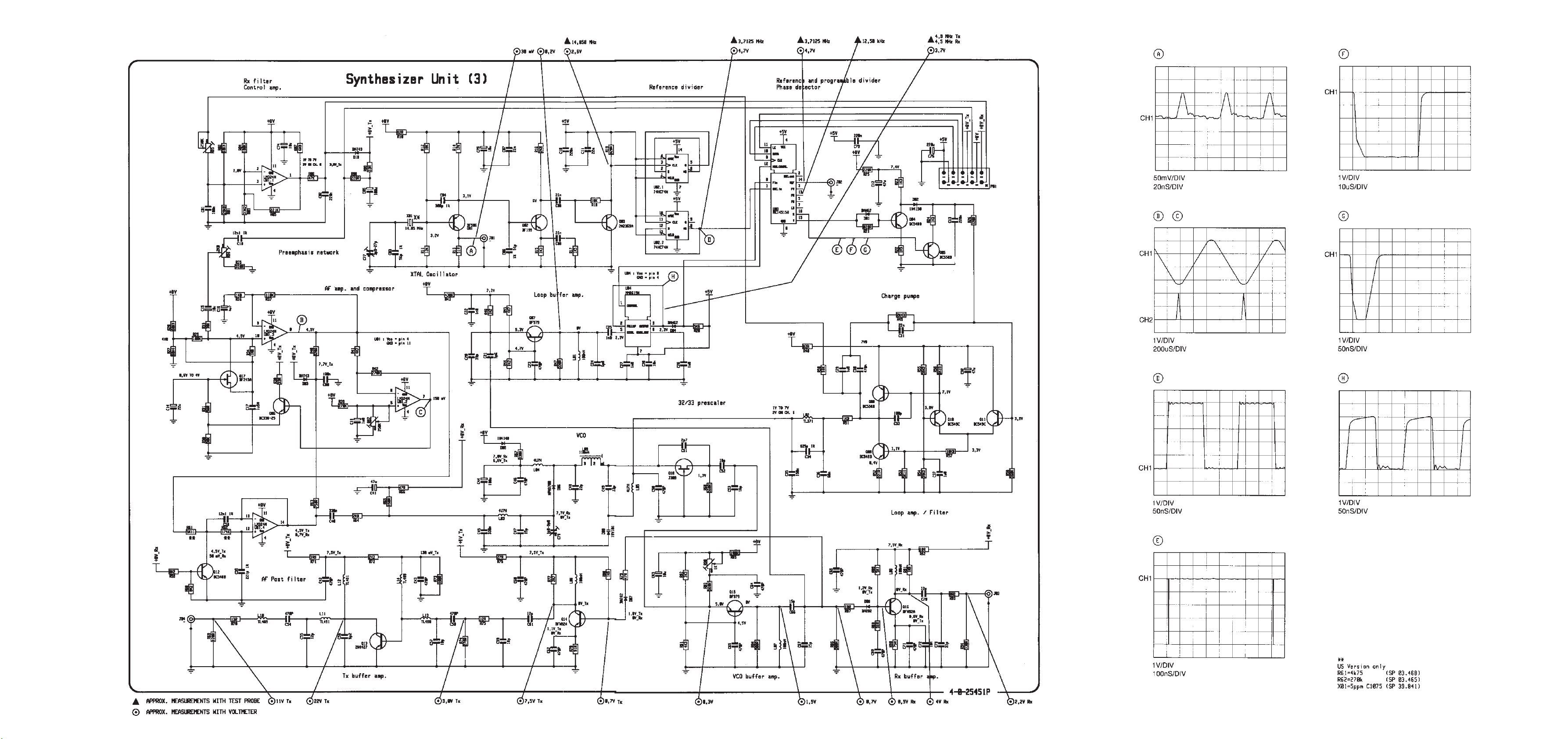
5.3. SYNTHESIZER UNIT (MODULE 3)
5.3.1. VCO with Buffer
The voltage controlled oscillator, built around the Field Effect Transistor Q18, is oscillating either on the transmitting
frequency or on the first receiver local oscillator frequency, which means the receiving frequency less 15.3 MHz.
To reach this function, the oscillator is implemented with a bandshift by means of the bandswitch diode D6 and the
two capacitors C47 and C78.
In transmit mode, where the diode D6 is reverse biased, the oscillating frequency is mainly determined by C48, L9,
C49, C51, and D9.
In receiving mode the oscillator resonance frequency is lowered 15.3 MHz by switching D6 on and thus putting C47
and C78 in parallel with C48.
The oscillating frequency is varied by means of the control voltage fed to the capacitor diode D9.
The output voltage from the VCO is taken via a capacitive tap C52, C53 on the source of Q18 and fed to the common
buffer amplifier, built around Q15. The power gain of this stage is adjusted by means of potentiometer R98. The
gain is adjusted so that the output level from the TX buffer amplifier is 200 mW measured at the output connector
J4.
5.3.2. loop Buffer Amplifier
The output from the common VCO buffer is fed to the divider chain via the stage around Q7, which secures the
needed amplification and the reverse isolation between the digital parts and the VCO.
The amplifier is a fixed tuned broad band amplifier with 11, C24, and R47 forming a low Q tuned circuit.
5.3.3. 32/33 Prescaler
The integrated circuit U4 is a two modulus prescaler based on the ECL technique.
From the Control logic in the programmable divider U3 pin 12, a high or low level is led to the prescaler U4 pin I.
A high level at U4 pin 1 causes the prescaler to divide by 33 and in turn a low level at pin I sets it up for dividing
by 32.
The resistor R20 and the diode D4 work as a speed-up and overdrive protection circuit.
5.3.4. Reference/Programmable Divider and Phase Detector
The integrated circuit U3 comprises both a programmable divider for the reference input and a programmable
divider with control logic for use in conjunction with a dual modulus prescaler. Besides, the IC includes two phase
detectors and a lock detector of which only one of the phase detectors is in use, the output pins located at pin 15
and pin 16.
Both dividers are programmed via the serial bus from the microcomputer. The coding structure of the serial data
stream includes the needed information for the on-chip decoder to detect the kind of the reached division figures.
The reference division ratio is constant as the input of 3.7125 MHz is derived from the X-tal oscillator.
In the beginning of a counting period the prescaler U4 starts dividing by 33. After a few counts the modulus control
pin changes level and the prescaler will finish the dividing cycles with a division ratio of 32, ending up with the correct
total division ratio.
The pulse frequency out of the reference divider is 12.5 kHz. If the VCO frequency is correct the pulse frequency
from the variable divider is also 12.5 kHz and in phase with the pulse from the reference divider. The on-chip phase
detector compares the phase of the two pulses. If they are out of phase the detector creates correction pulses to
the Charge Pumpe for correction of the VCO frequency/phase.
However, the synthesizer circuit is made with a small constant phase error, forced by the current drawn through
R58, to avoid phase detector non linearities to degrade the loop performance. So the phase detector is sending
small correction pulses to transistor Q4 with a frequency of 12.5 kHz.
5.3.5. Charge Pumpe
The charge pumpe, mainly consisting of Q4, Q5, and D2, converts the pulse with modulated phase detector outputs
of U3 pin 15 and 16 to a DC current flowing into or out of the loop amplifier.
Assume that the VCO frequency has decreased from its nominal value. The phase detector will produce a negative
correction pulse on pin 16, turning Q5 on, resulting in current being drawn out of the loop amplifier.
This action will cause the output voltage to increase, thus increasing the VCO frequency to the nominal value.
An increase in VCO frequency from its nominal value will in turn cause a correction pulse on pin 15, turning Q4 off,
resulting in current flowing into the loop amplifier through the diode D2. This means the output voltage will decrease,
forcing the VCO frequency to decrease.
Because of the current drawn through R58, a small correction pulse of about 500 nsec. will always be present at
pin 15 on U3 with a frequency of 12.5 kHz.
Page 5-6

5 CIRCUIT DESCRIPTION AND SCHEMATIC DIAGRAMS RT2048RT2048
5.3.6. Loop Amplifier/Filter
The loop amplifier is realized as a discrete operational amplifier with transistors Q10 and Q11 forming the input
differential pair and Q8, Q9 the output stage.
The loop dynamic performance is mainly controlled via the feed-back components in the loop amplifier, this means
capacitors C29, C30, C31 and R49. The output from the loop amplifier is further filtered in a low pass filter formed
by C36, L2, C34, and C35, to reduce the level of the reference frequency sidebands on the VCO output.
5.3.7. RX Buffer Amplifier
When receiving, the bandswitch diode D8 is turned on, and the output from the VCO buffer amplifier is further
amplified in a single tuned amplifier formed around Q16 with L8, C70, and C73 forming the tuned circuit. The output
is attenuated and impedance matched by means of resistors R93 and R94. The typical output level at connector
J3 will be 5 mW.
5.3.8. TX Buffer Amplifier
When the set changes to transmit mode, the band switch diode D7 will be turned on and the output from the VCO
buffer amplifier will be fed to the two stage amplifier circuit.
The level is amplified to about 30 mW in Q14 and the final stage with Q13 boosts the level to about 200 mW
measured at connector J4.
The first stage is working as a class A amplifier with the base on Q14 biased through R80, D7, R79, and R86. The
output stage is working as a class C amplifier with a small base bias through resistors R72 and R73.
5.3.9. X-Tal Oscillator
The oscillator is of a Colpitt type and the oscillator transistor Q1 is oscillating by means of a 14.850 MHz crystal
X1.
The trimmer capacitor C77 is for fine adjustment of the oscillator frequency.
RF signal for the second mixer in the receiver is taken from the collector of transistor Q1, connector J1. The oscillator
signal is buffered and amplified in transistors Q2 and Q3 before it is fed to the reference divider.
5.3.10. Reference Divider
The fixed divide by four reference divider U2 divides the X-tal oscillator frequency down to 3.7125 MHz before it
is fed to the microcomputer via connector J2 and the phase locked loop reference divider included in U3.
5.3.11. RX Filter Control Amplifier
This variable slope DC amplifier made by means of an operational amplifier U1 converts the VCO control voltage
to an appropriate control voltage for the variocap. diode tuned filters in the receiver front-end.
The maximum output voltage is adjusted by means of potentiometer R95.
5.3.12. Preempbasis Network
Capacitor C18 in conjunction with R35 and R96 introduces the needed 6 dB/oct. response of the AF input signal.
The input sensitivity is adjusted by means of R96.
5.3.13. AF Amplifier/Compressor
This circuit, formed around two operational amplifiers in U1, comprises both an amplifying and voltage limiting
function. Amplifier No. 3 is a fixed voltage amplifier, the output of which is sensed by means of the comparator made
by amplifier No. 2. When the peak output voltage exceeds a certain level, adjusted by means of potentiometer R97,
the comparator will turn on transistor Q6, which in turn will charge capacitor C14. So the gate-source voltage on
transistor Q17, acting as a variable resistor, will decrease and also the AC resistance between pin 10 on U1 and
ground, which in turn will reduce the input level to the amplifier.
The rise-time of the compressor is mainly determined by resistors R38, R31, and capacitor C14. The decay-time
by C14 and R30.
5.3.14. AF Post Filter
This second order active filter, built around operational amplifier No. 4 in U1, secures an appropriate high frequency
roll-off of the AF signal. Resistors R64 and R65 give an appropriate attenuation of the AF signal before it is fed to
the modulating diode D6 in the VCO.
Page 5-7

5 CIRCUIT DESCRIPTION AND SCHEMATIC DIAGRAMS RT2048
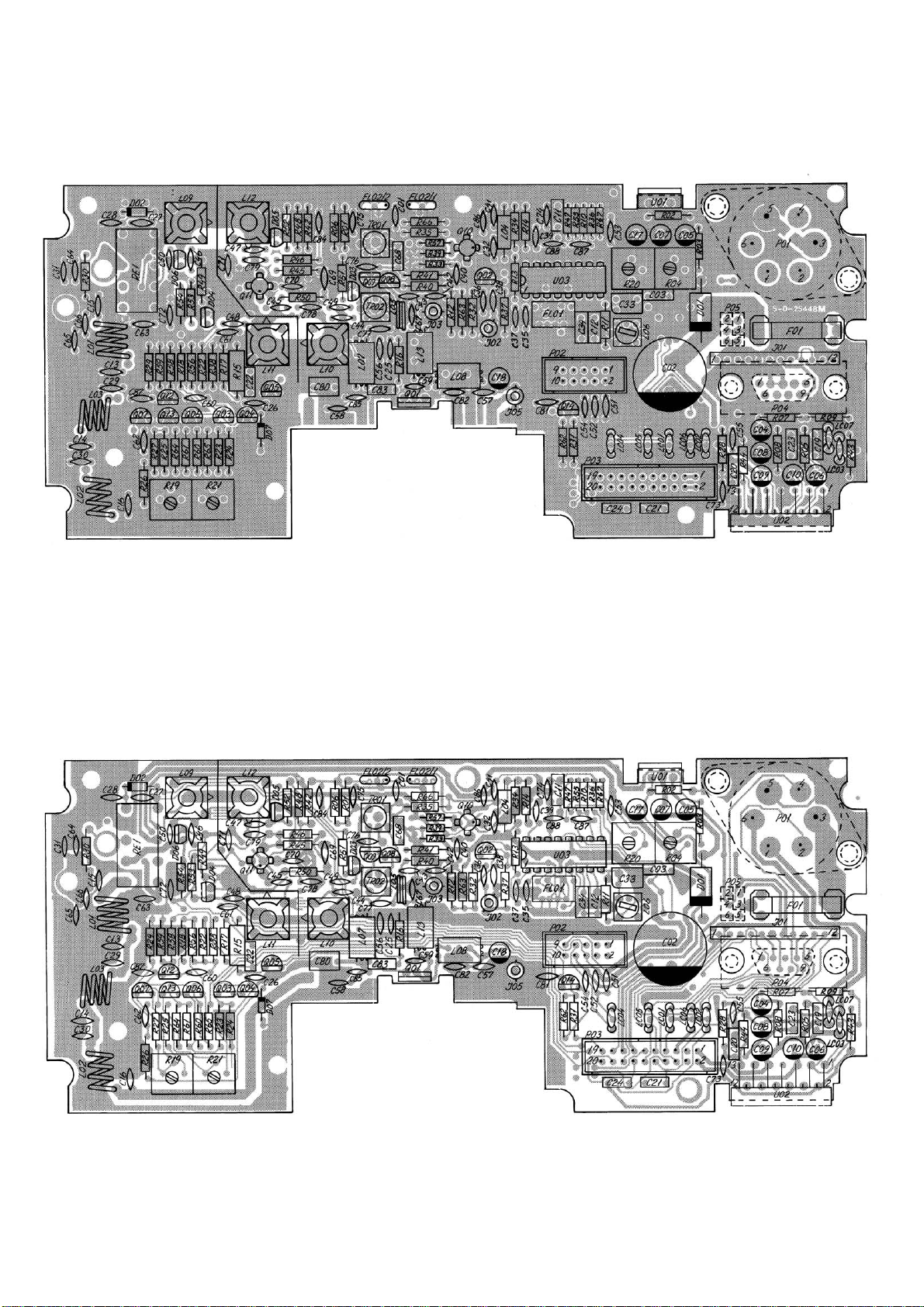
SYNTHESIZER (MODULE 3)
View from component side with upper side tracks.
PCB rev. 25448M
View from component side with lower side tracks.
PCB REV. 25451H
Page 5-8
5 CIRCUIT DESCRIPTION AND SCHEMATIC DIAGRAMS
SYNTHESIZER UNIT MODULE 3
RT2048
9519
This diagram is valid for PCB rev. 25451H
Page 5-9

5 CIRCUIT DESCRIPTION AND SCHEMATIC DIAGRAMS RT2048
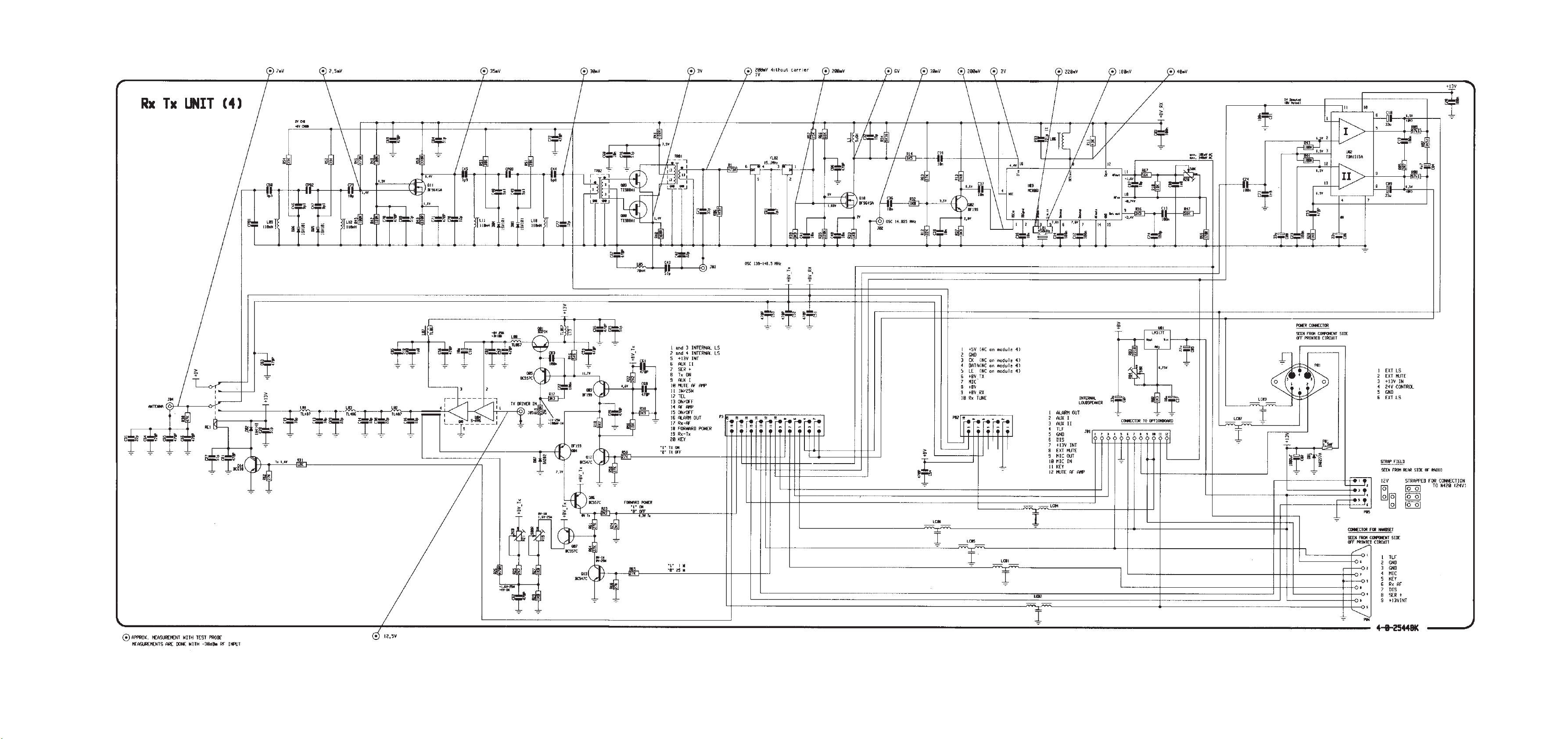
5.4. RX/TX UNIT (MODULE 4)
The RX/TX unit comprises the following circuits:
The receiver including detector
AF power amplifier
RF power amplifier
Harmonic filter
RF power control
8V power supply
5.4.1. RECEIVER FRONT-END
The RF amplifier covers the frequency range 154.400 MHz to 163.600 MHz and consists of the low noise
Dual Gate Si-Mos-FET Q11 surrounded by two high Q double-tuned bandpass filters.
From the aerial the signal is led through the aerial relay to the receiver input bandpass filter. The input
bandpass filter as well as the intermediate bandpass filter are controlled by a DC voltage on the tuning diodes.
This DC voltage derives from the RX VCO control voltage and secures an optimum filter response in the
whole frequency range of the receiver.
The two bandpass filters create the necessary attenuation of unwanted signals.
5.4.2. FIRST MIXER
The balanced mixer has good large signal properties, securing good intermodulation characteristic.
The mixer transistors Q08 and Q09 are of the J-FET type.
The signal is led to the balanced input transformer TR2 and then to the gates of the J-FETS, which are
switched by injecting the first LO signal into the sources. The mixed signals are fed to the balanced output
transformer TR1 where the wanted signal on 15.3 MHz is selected by the tune circuit consisting of TR1 and
C75.
R06 and R01 create the necessary impedance matching the IF crystal filter.
5.4.3. CRYSTAL FILTER
The receiver adjacent channel selectivity is maintained by means of the crystal filter FL2 in co-operation with
the ceramic filter FL1. R57 and R39 give the impedance matching the crystal filter output.
5.4.4. IF AMPLIFIER
The transistor Q10 amplifies the signal to the 2nd mixer, which has a tuned drain circuit consisting of L04
and C32. R34 creates the impedance matching the 2nd mixer.
5.4.5. SECOND MIXER, CERAMIC FILTER, DETECTOR AND AF AMPLIFIER
The second LO signal 14.850 MHz is amplified in Q02 before it is delivered to the mixer.
The signal out of the mixer (450 kHz) is fed through the ceramic filter to the limiter amplifier and discriminator
in U03.
The phase shift network to the quadrangular discriminator consisting of R11, L06, C33, and a 10 pF capacitor
inside the IC.
AF output is led through a lowpass filter consisting of R36 and C74, which removes the high frequencies (450
kHz).
An internal operational amplifier amplifies the AF signal to 250 mV, which is adjusted by R20.
5.4.6. AF POWER AMPLIFIER
The AF power amplifier is capable of delivering 6 Watt in the internal loudspeaker (4 ohm) and 6 Watt in an
external loudspeaker 4 ohm.
The gain of 34 dB is fixed by the resistors R07, R08 and R09.
The AF power amplifier is muted (pin 11, 0 = off, 1 = on) about 1.25 sec. after the squelch is closed.
5.4.7. RF POWER AMPLIFIER
The power amplifier covering the frequency range 154.4 MHz to 163.6 MHz consists of a module with 50 ohm
terminations and 2 amplifiers. The first amplifier is the driver which has a gain of up to 12 dB, depending
on the driver voltage from Q01. The input is about 200 mW.
The second amplifier has a gain of 10 dB.
5.4.8. HARMONIC FILTER
The harmonic filter is realized as a seventh order Chebyscher filter, which at the same time will provide the
necessary attenuation of the harmonic generated by the power amplifier and a low insertion loss at the carrier
frequency.
The output is fed to the antenna relay.
Page 5-10

5 CIRCUIT DESCRIPTION AND SCHEMATIC DIAGRAMS RT2048
5.4.9. RF POWER CONTROL
The power adjustment loop consists of Q04, Q03, Q05 and Q1.
Q04 is the power detector which together with Q03 forms a differential circuit.
The differential circuit controls Q05 and Q01 which are made as a Darlington transistor.
C22, R17, and R15 make a feed-back in order to slow down the loop.
Q12 controls the on/off function through the differential resistor R18.
Q06 is the power indicator transistor which gives the microcomputer information about power on the output from
the RF power amplifier.
This information is active about 0.3 Watt.
Q13 controls the 1 Watt/25 Watt change-over transistor Q07. If the power is lower than about 15 Watt in the 25 Watt
position the power indicator transistor Q06 will make a smooth change-over to 1 Watt position through resistor R61.
The 25 Watt adjustment is done on R21 and the 1 Watt adjustment is done on R19. The 25 Watt has to be adjusted
first because it has influence on the adjustment of 1 Watt.
5.4.10. 8V POWER SUPPLY
The regulator U01 is supplied from the internal 13V supply.
The adjustment of the voltage is done on resistor R04.
The 8V supply is divided into 2 more supplies in the antenna relay, the 8V TX supply and the 8 RX supply.
Page 5-11
5 CIRCUIT DESCRIPTION AND SCHEMATIC DIAGRAMS RT2048
Rx/Tx UNIT (MODULE 4)
View from component side with upper side tracks.
View from component side with lower side tracks.
PCB rev. 25448M
Page 5-12
9804
5 CIRCUIT DESCRIPTION AND SCHEMATIC DIAGRAMS RT2048
Rx/Tx UNIT MODULE4
This diagram is valid for PCB rev. 25448M
Page 5-13

5 CIRCUIT DESCRIPTION AND SCHEMATIC DIAGRAMS RT2048
5.5. SELCALL UNIT (MODULE 5)
The input to the selcall is taken from the telephone output. The signal is first amplified and limited in U04/
2 and then it passes the bandpass filter. Finally the signal is rectified and compared with a reference level
in the comparator U04/1.
3.7125 MHz is divided in the programmable counter U06. The output of, this is divided by 2 and turned into
a square wave in the flip-flop U03/2. The outputs of the flip-flop is connected to the switches U02. The
frequency, at which the switches around the capacitors C03 and C04 are working, determines the resonance
frequency of the filter. Thus by changing the dividing figure to U06, it is possible to change the resonance
frequency of the filter.
With R01 it is possible to fine adjust the resonance frequency of the filter (see the adjustment procedure).
Figure f(nominal) U06 input U03 output
No. (Hz) 14 13 12 11 6543 (Hz)
1 1124 01100111 18022
2 1197 01100000 19336
3 1275 01011010 20625
4 1358 01010101 21838
5 1446 01010000 23203
6 1540 01001011 24750
7 1640 01000110 26518
8 1747 01000010 28125
9 1860 00111110 29940
0 1982 00111010 32004
R 2110 00110111 33750
When the radio is switched on the dividing figure, corresponding to the first figure in the selcall number, is
shifted out on port B0 on the uC at the interface unit which is connected to the input of U07. U07 is a serial
to parallel shift register which converts the signal to the dividing figure U06. If the correct tone is received
the output of the comparator U4/1 goes low. This output is connected to the uC’s SEL-DET. pin. When the
tone disappears again the uC will put out the dividing figure corresponding to the next figure in the selcall
number.
If all five tones are received correctly, the port C06 (EXT. ALARM) on the uC goes high. This port is connected
to pin I on the connector to the option board at the RX/TX unit. At the same time the uC will send out an alarm
tone from D06 via the volume control and power amplifier to the loudspeaker. The alarm tone lasts for 10
secs after an individual call, and after an all call it lasts until the selcall has been reset. If the SELCALL
T/R button is activated the alarm circuits and indicators are tested.
Page 5-14

5 CIRCUIT DESCRIPTION AND SCHEMATIC DIAGRAMS RT2048
View from component side with upper side tracks.
PCB REV. 25449B
View from component side with lower side tracks.
Page 5-15
5 CIRCUIT DESCRIPTION AND SCHEMATIC DIAGRAMS RT2048
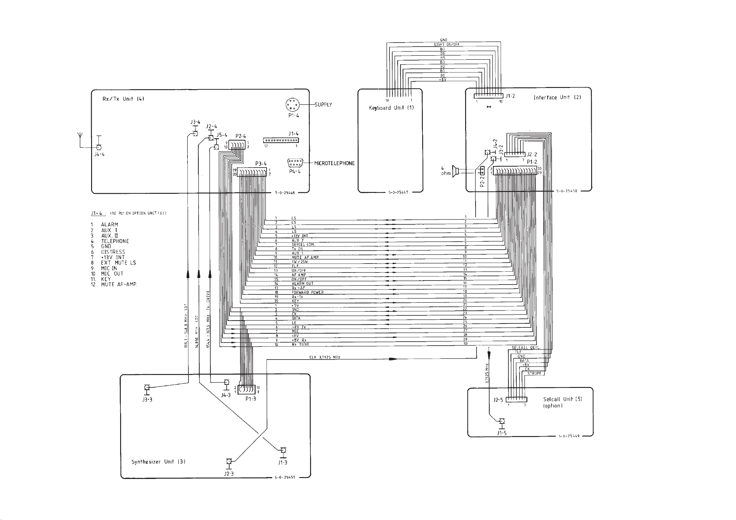
5.6. INTERCONNECTION CABLE DIAGRAM
4-0-25558B
RT2048B
Page 5-16

RT2048
CONTENTS
6. MICROTELEPHONE INSTALLATION 6-1
6.1. SPECIAL INSTALLATION WITH 2 MICROTELEPHONES 6-3
6.2. SPECIAL INSTALLATION WITH 3 MICROTELEPHONES 6-4
6.3. MECHANICAL DIMENSIONS FOR HANDSET 6-5
9350


5
9
1
6
7
3
5
2
4
1
6
MC801
MIC PRE-AMP
WHITE
P803
DIN
CONNECTOR
BLUE
TC801
RED
YELLOW
BROWN
HAND KEY
S801
VHF RT2047 SCRAMBLER CRY2001, RE2100, RT2047 prepared for DSC and RT2048
S1
HAND KEY
YELLOW
RED
TC1
MIC PRE-AMP
MC1
D-CONNECTOR
BLUE
WHITE
BROWN
SHORTWAVE S130X
S1701
HAND KEY
BROWN
WHITE
RED
TC1701
BLUE
CONNECTOR
HIRSCHMANN
P1701
YELLOW
MIC PRE-AMP
MC1701
6
1
4
2
5
3
MC1
R1
1k8
C1
100u
10nC2D1
1N4148
8k2
R3
R5
2k7
2k2
R7
R9
2k7
R10
120k
R2
1k8
*
C3
10u
u47
C4
R4
18k
MIC. PRE-AMPLIFIER (100)
33u
C10
39k
R11
4k7
R6
C5
2u2
2u2
C6
R8
6k8
C9
1n
10u
C7
1n
C8
C11
10n
390 +10-18v
For TEST
4-0-24025E
In orange marked microtelephone cartridge, R2 is changed from 1k8 to 5k6 ohm.
10mV/DIV
OV
0.5msec/DIV 0.5msec/DIV
OV
10mV/DIV
T3
BC547C
BC547C
T2
BC547C
T1
27777A
C12
27pf
C13
27pf
C14
15pf
C14
15pf
C4 C5C10
C6
C7
T2
T3
T1
C1
C3
R3
R2
R5
R11
R1
R7
R10
R9
D1
C2
C9
R4
R6
R8
C8
C11
C13
C12
6. MICROTELEPHONE INSTALLATION
RT2048
RT2048 5-0-24025D
9649
Page 6-1

6 MICROTELEPHONE INSTALLATION RT2048
MICROTELEPHONE WITH ELECTRET MIC. AMP. ECI A/S 4-6-24025D/4-0-24025E 600875
POSITION DESCRIPTION MANUFACTOR TYPE PART NR.
C1 CAPACITOR ELECTROLYTIC 100uF 20% 10VDC ERO EKI 00 BB 310 C M0E 14.607
C2 CAPACITOR CERAMIC 10nF -20/+80% CL2 50VDC KCK RT-HE70 SK YF 103 Z 15.170
C3 CAPACITOR ELECTROLYTIC 10uF 20% 35VDC ELNA RJ2-35-V-100-M-T34(T58) 14.512
C4 CAPACITOR ELECTROLYTIC 0.47uF 20% 50VDC ELNA RJ3-50-V-R47-M-T34 14.504
C5 CAPACITOR ELECTROLYTIC 2u2F 20% 50VDC ELNA RJ2-50-V-2R2-M-T34 14.503
C6 CAPACITOR ELECTROLYTIC 2u2F 20% 50VDC ELNA RJ2-50-V-2R2-M-T34 14.503
C7 CAPACITOR ELECTROLYTIC 10uF 20% 35VDC ELNA RJ2-35-V-100-M-T34(T58) 14.512
C8 CAPACITOR CERAMIC CL2 1n0F 10% 100V PHILIPS 2222 630 63102 16.149
C9 CAPACITOR CERAMIC CL2 1n0F 10% 100V PHILIPS 2222 630 63102 16.149
C10 CAPACITOR ELECTROLYTIC 33uF 20% 16VDC ELNA RJ2-16-V-330-M-T34 14.518
C11 CAPACITOR CERAMIC 10nF -20/+80% CL2 50VDC KCK RT-HE70 SK YF 103 Z 15.170
C12 CAPACITOR CERAMIC 27pF 10% N750 500VDC KCK RT-HM60-SK UJ 270 K 16.062
C13 CAPACITOR CERAMIC 27pF 10% N750 500VDC KCK RT-HM60-SK UJ 270 K 16.062
C14 CAPACITOR CERAM. SMD 0805 15pF 5% NPO 50VDC MURATA GRM40 COG 150 J 50 PT 323.076
D1 DIODE 1N4148 HIGH SPEED PHILIPS 1N4148-143 25.131
MC1 MICROPHONE ELECTRET ›9.7 x 6.7mm PANASONIC WM-0344BY 46.012
R1 RESISTOR MF 1k8 OHM 5% 0.33W PHILIPS 2322 187 73182 02.478
R2 RESISTOR MF 1k8 OHM 5% 0.33W PHILIPS 2322 187 73182 02.478
R3 RESISTOR MF 8k2 OHM 5% 0.33W PHILIPS 2322 187 73822 02.494
R4 RESISTOR MF 18k OHM 5% 0.33W PHILIPS 2322 187 73183 02.502
R5 RESISTOR MF 2k7 OHM 5% 0.33W PHILIPS 2322 187 73272 02.482
R6 RESISTOR MF 4k7 OHM 5% 0.33W PHILIPS 2322 187 73472 02.488
R7 RESISTOR MF 2k2 OHM 5% 0.33W PHILIPS 2322 187 73222 02.480
R8 RESISTOR MF 6k8 OHM 5% 0.33W PHILIPS 2322 187 73682 02.492
R9 RESISTOR MF 2k7 OHM 5% 0.33W PHILIPS 2322 187 73272 02.482
R10 RESISTOR MF 120k OHM 5% 0.33W PHILIPS 2322 187 73124 02.522
R11 RESISTOR MF 39k OHM 5% 0.33W PHILIPS 2322 187 73393 02.510
S1 MICROSWITCH E62-10H PDT CHERRY E62-10H PDT 44.025
T1 TRANSISTOR AF NPN BC547C TO-92 PHILIPS BC547C-126 28.068
T2 TRANSISTOR AF NPN BC547C TO-92 PHILIPS BC547C-126 28.068
T3 TRANSISTOR AF NPN BC547C TO-92 PHILIPS BC547C-126 28.068
TC1 TRANSDUCER DYNAMIC FOR HANDSET •31x18mm 200 OHM S.E.K. (KIRK) T802 0113 2715 46.010
Page 6-2
9649
6.1. SPECIAL INSTALLATION WITH 2 MICROTELEPHONES:
H2086 FOR SCRAMBLER CRY2001 AND RT2048
H2087 FOR VHF RT2047 AND SSB T2031
MICROTELEPHONE ONE WITH PREFERENCE
RT2048
Page 6-3

6 MICROTELEPHONE INSTALLATION RT2048
6.2. SPECIAL INSTALLATION WITH 3 MICROTELEPHONES:
H2088 FOR SCRAMBLER CRY2001 AND RT2048
H2089 FOR VHF RT2047 AND SSB T2031
MICROTELEPHONE ONE WITH PREFERENCE
4-0-24804A
Page 6-4

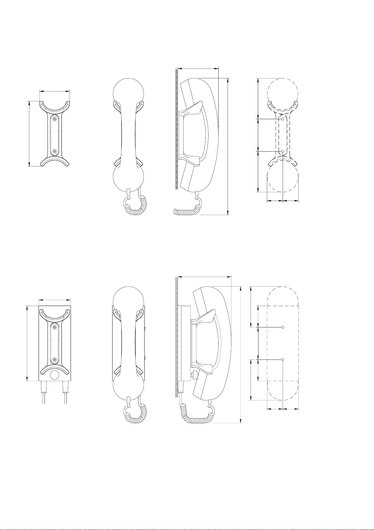
6.3. MECHANICAL DIMENSIONS FOR HANDSET
64
151
RT2048
81
80
436543
ø4.5
27946
MECHANICAL DIMENSIONS FOR HANDSET HOLDER WITH MICROSWITCH
4-0-26999 4-0-27946
RT2048, RE2100, C2140
64
103
275
ø4.5
80
32 32
80
436543
ø4.5
151
26999
275
ø4.5
80
32 32
Page 6-5
6 MICROTELEPHONE INSTALLATION RT2048
MECHANICAL DIMENSIONS FOR HANDSET
78
62
ø4.5
132
275
4-0-29938
MECHANICAL DIMENSIONS FOR HANDSET HOLDER WITH MICROSWITCH
103
64
65 8080
ø4.5
32 32
8080
43
ø4.5
151
Page 6-6
4-0-29937
275
6543
ø4.5
32 32
9438

RT2048
CONTENTS
7. PARTS LIST 7-1
9350


RT2048
7. PARTS LIST
SIMPLEX / SEMIDUPLEX VHF RT2048 STANDARD ECI A/S VHF RT2048 (STANDARD) 802048
POSITION DESCRIPTION MANUFACTOR TYPE PART NO.
VARIOUS KEYBOARD FOIL RT2048 ECI A/S 1-0-25434C 225434
VARIOUS MINI 1/4 BOX CABINET SAILOR GREEN 225435 GRØN RILSAN 22543500
VARIOUS POWER CABLE WITH PLUG ECI A/S 503758 POWERKABEL 503758
VARIOUS BASE UNIT RT2048 STD. ECI A/S 702048
VARIOUS MICROTELEPHONE w. CRADLE CRY2001/RE2100/RT2048 ECI A/S 3-0-25772 725772
VARIOUS ECI A/S GRØN 727206
VARIOUS AERIAL PLUG PL259 RODAN PL259/LODDE/BAKELIT INDL. 78 .502
VARIOUS OPERATION INSTRUCTIONS RT2048 ECI A/S B2048
VARIOUS SERVICE AND SALES AGENTS ADRESSES WORLD WIDE ECI A/S F1000GB
VARIOUS MANUAL RT2048 ENGLISH ECI A/S M2048GB
-SPEC BUS-INTERRUPT OPTION (6) RM2042 ECI A/S 5-0-26945B / 4-0-26945 626945
SIMPLEX / SEMIDUPLEX VHF RT2048 USA ECI A/S VHF RT2048 (USA) 812048
POSITION DESCRIPTION MANUFACTOR TYPE PART NO.
VARIOUS KEYBOARD FOIL RT2048 ECI A/S 1-0-25434C 225434
VARIOUS MINI 1/4 BOX CABINET SAILOR GREEN 225435 GRØN RILSAN 22543500
VARIOUS FRONTPLATE RT2048 SAILOR GREEN ECI A/S 141A764 LAK 22544000
VARIOUS SILICONE SEAL FOR CABINET NORD.ELEKTR. 0-4-25397A 48.585
VARIOUS KNOB Ø10mm SANDER PLAST 0-3-25432A 48.693
VARIOUS KNOB Ø30mm SANDER PLAST TG.NR.:0-3-25433B 48.694
VARIOUS FUSE COVER SANDER PLAST Tg.Nr: 0-3-25362B 48.696
VARIOUS COVER FOR ALLEN SCREW SANDER PLAST 0-3-25350A 48.699
VARIOUS POWER CABLE WITH PLUG ECI A/S 503758 POWERKABEL 503758
VARIOUS CONNECTION CABLE FOR LOUDSPEAKER AFD.32 3-0-25463 525463
VARIOUS MAIN INTERCONNECTION CABLE RT2048 3M 3-0-25462B 56.004
VARIOUS MICROTELEPHONE w. CRADLE CRY2001/RE2100/RT2048 ECI A/S 3-0-25772 725772
VARIOUS AERIAL PLUG PL259 RODAN PL259/LODDE/BAKELIT INDL. 78 .502
VARIOUS ANTENNA JACK (FEMALE) SO239 KAJ V HANSEN SO239 78.504
VARIOUS SCREW PT Ø2.9 x 16MM A2 EJOT GMBH KB30x16 WN-1442/A2 88.103
VARIOUS OPERATION INSTRUCTIONS RT2048 ECI A/S B2048
VARIOUS SERVICE AND SALES AGENTS ADRESSES WORLD WIDE ECI A/S F1000GB
VARIOUS MANUAL RT2048 ENGLISH ECI A/S M2048GB
VARIOUS COAX CABLE Ø3x23cm ECI A/S 3-0-25471 525471
VARIOUS COAX CABLE Ø3x23cm ECI A/S 3-0-25471 525471
-1 KEYBOARD MODULE RT2048 ECI A/S 5-0-25447 625 447
-2 INTERFACE MODULE RT2048 ECI A/S 5-0-25450L / 4-0-25450N 62 5450
-3 SYNTESE MODULE (USA) RT2048 ECI A/S 5-0-25451H / 4-0-25451N 625551
-4 RX/TX MODULE RT2048 ECI A/S 5-0-25448M / 4-0-25448K 625448
-5 SELCALL MODULE (OPTIONAL) RT2048 ECI A/S 5-0-25449B / 4-0-25449D 62544 9
-SPEC BUS-INTERRUPT OPTION (6) RM2042 ECI A/S 5-0-26945B / 4-0-26945 626945
VARIOUS MICROTELEPHONE FOR CRY2001, RT2048 & RE2100 ECI A/S 700118 MICROTELEPHONE 700118
LS1 LOUDSPEAKER 4 OHMS 15W 88x88mm RIGHT ELEC. S-881252-035P 46.052
ALUMINIUM
632-2456-00-X
SIMPLEX / SEMIDUPLEX VHF RT2048 NEDERLAND (10) ECI A/S VHF RT2048 NL (10) 832048
POSITION DESCRIPTION MANUFACTOR TYPE PART NO.
VARIOUS MINI 1/4 BOX CABINET SAILOR GREEN 225435 GRØN RILSAN 22543500
VARIOUS KEYBOARD FOIL RT2048 NEDERLAND (10) ECI A/S 1-0-26179 226179
VARIOUS POWER CABLE WITH PLUG ECI A/S 503758 POWERKABEL 503758
VARIOUS STICKER “BV” MELSEN 9-3-24436 53.248
VARIOUS BASE UNIT RT2048 STD. ECI A/S 702048
VARIOUS MICROTELEPHONE w. CRADLE CRY2001/RE2100/RT2048 ECI A/S 3-0-25772 725772
ECI A/S GRØN 727206
VARIOUS AERIAL PLUG PL259 RODAN PL259/LODDE/BAKELIT INDL. 78 .502
VARIOUS OPERATION INSTRUCTIONS RT2048 ECI A/S B2048
VARIOUS SERVICE AND SALES AGENTS ADRESSES WORLD WIDE ECI A/S F1000GB
VARIOUS MANUAL RT2048 ENGLISH ECI A/S M2048GB
-SPEC BUS-INTERRUPT OPTION (6) RM2042 ECI A/S 5-0-26945B / 4-0-26945 626945
9724
ALUMINIUM
Page 7-1

7 PARTS LIST RT2048
SIMPLEX / SEMIDUPLEX VHF RT2048 (RHEIN) S.P. RADIO A/S VHF RT2048 (RHEIN) 842048
POSITION DESCRIPTION MANUFACTOR TYPE PART NO.
VARIOUS MINI 1/4 BOX CABINET SAILOR GREEN 225435 GRØN RILSAN 22543500
VARIOUS KEYBOARD FOIL RT2048 NEDERLAND (16) ECI A/S 1-0-25577 225577
VARIOUS POWER CABLE WITH PLUG ECI A/S 503758 POWERKABEL 503758
VARIOUS STICKER “BV” MELSEN 9-3-24436 53.248
VARIOUS BASE UNIT RT2048 STD. ECI A/S 702048
VARIOUS MICROTELEPHONE w. CRADLE CRY2001/RE2100/RT2048 ECI A/S 3-0-25772 725772
ECI A/S GRØN 727206
VARIOUS ATIS OPTION FOR RT2048 ECI A/S 0-0-28665 728665
VARIOUS AERIAL PLUG PL259 RODAN PL259/LODDE/BAKELIT INDL. 7 8.502
VARIOUS OPERATION INSTRUCTIONS RT2048 ECI A/S B2048
VARIOUS SERVICE AND SALES AGENTS ADRESSES WORLD WIDE ECI A/S F1000GB
VARIOUS MANUAL RT2048 ENGLISH ECI A/S M2048GB
ALUMINIUM
Page 7-2
9724

7 PARTS LIST RT2048
BASE UNIT RT2048 STD. ECI A/S 702048
POSITION DESCRIPTION MANUFACTOR TYPE PART NO.
VARIOUS SILICONE SEAL FOR CABINET NORD.ELEKTR. 0-4-25397A 48.585
VARIOUS KNOB Ø10mm SANDER PLAST 0-3-25432A 48.693
VARIOUS FUSE COVER SANDER PLAST Tg.Nr: 0-3-25362B 48.696
VARIOUS COVER FOR ALLEN SCREW SANDER PLAST 0-3-25350A 48.699
VARIOUS CONNECTION CABLE FOR LOUDSPEAKER AFD.32 3-0-25463 525463
VARIOUS MAIN INTERCONNECTION CABLE RT2048 3M 3-0-25462B 56.004
VARIOUS ANTENNA JACK (FEMALE) SO239 KAJ V HANSEN SO239 78.504
VARIOUS SCREW PT Ø2.9 x 16MM A2 EJOT GMBH KB30x16 WN-1442/A2 88.103
VARIOUS COAX CABLE Ø3x23cm ECI A/S 3-0-25471 525471
VARIOUS COAX CABLE Ø3x23cm ECI A/S 3-0-25471 525471
-1 KEYBOARD MODULE RT2048 ECI A/S 5-0-25447 625 447
-2 INTERFACE MODULE RT2048 ECI A/S 5-0-25450K / 4-0-25450N 6254 50
-3 SYNTESE MODULE RT2048 ECI A/S 5-0-25451H / 4-0-25451P 625451
-4 RX/TX MODULE RT2048 ECI A/S 5-0-25448L / 4-0-25448K 6 25448
-5 SELCALL MODULE (OPTIONAL) RT2048 ECI A/S 5-0-25449B / 4-0-25449D 62544 9
VARIOUS MICROTELEPHONE FOR CRY2001, RT2048 & RE2100 ECI A/S 700118 MICROTELEPHONE 700118
LS1 LOUDSPEAKER 4 OHMS 15W 88x88mm RIGHT ELEC. S-881252-035P 46.052
632-2456-00-X
KEYBOARD MODULE RT2048 ECI A/S 5-0-25447 625447
POSITION DESCRIPTION MANUFACTOR TYPE PART NO.
D1-1 DIODE LIGHT EMITTING SUB MINIATURE YELLOW H.P. HLMP-7019 25.649
D2-1 DIODE LIGHT EMITTING SUB MINIATURE YELLOW H.P. HLMP-7019 25.649
D3-1 DIODE LIGHT EMITTING SUB MINIATURE YELLOW H.P. HLMP-7019 25.649
D4-1 DIODE LIGHT EMITTING SUB MINIATURE YELLOW H.P. HLMP-7019 25.649
D5-1 DIODE LIGHT EMITTING SUB MINIATURE YELLOW H.P. HLMP-7019 25.649
D6-1 DIODE LIGHT EMITTING SUB MINIATURE YELLOW H.P. HLMP-7019 25.649
J1-1 INTERCONNECTION CABLE 10 POLES L=60mm MOLEX 3-0-25465B 56.003
R1-1 RESISTOR MF 330 OHM 5% 0.4W PHILIPS 2322 181 53331 01.187
R2-1 RESISTOR MF 330 OHM 5% 0.4W PHILIPS 2322 181 53331 01.187
S1-1 SWITCH KEYBOARD 12x12mm ALPS SKHCAD (KHC 10904) 43.601
S2-1 SWITCH KEYBOARD 12x12mm ALPS SKHCAD (KHC 10904) 43.601
S3-1 SWITCH KEYBOARD 12x12mm ALPS SKHCAD (KHC 10904) 43.601
S4-1 SWITCH KEYBOARD 12x12mm ALPS SKHCAD (KHC 10904) 43.601
S5-1 SWITCH KEYBOARD 12x12mm ALPS SKHCAD (KHC 10904) 43.601
S6-1 SWITCH KEYBOARD 12x12mm ALPS SKHCAD (KHC 10904) 43.601
S7-1 SWITCH KEYBOARD 12x12mm ALPS SKHCAD (KHC 10904) 43.601
S8-1 SWITCH KEYBOARD 12x12mm ALPS SKHCAD (KHC 10904) 43.601
S9-1 SWITCH KEYBOARD 12x12mm ALPS SKHCAD (KHC 10904) 43.601
S10-1 SWITCH KEYBOARD 12x12mm ALPS SKHCAD (KHC 10904) 43. 601
S11-1 SWITCH KEYBOARD 12x12mm ALPS SKHCAD (KHC 10904) 43. 601
S12-1 SWITCH KEYBOARD 12x12mm ALPS SKHCAD (KHC 10904) 43. 601
INTERFACE MODULE RT2048 ECI A/S 4-6-25450L / 4-0-25450P 625450
POSITION DESCRIPTION MANUFACTOR TYPE PART NO.
VARIOUS SOCKET DIL 2x20 POLES AMP 641606-3 30.935
VARIOUS CONNECTION CABLE FOR VOLUME CONTROL RT2048 ECI A/S 3-0-25466 525466
VARIOUS SOCKET 1/10" SIL 10 POLES PRECI-DIP 311-91-110 78.803
C1-2 CAPACITOR MKT 150nF 5% 50VDC ERO MKT 1826-415/06 4-G 11 .181
C2-2 CAPACITOR ELECTROLYTIC 10uF 20% 35VDC ELNA RJ2-35-V-100-M-T58 14.512
C3-2 CAPACITOR POLYPROPYLENE 2n2F 5% 100VDC ERO KP 1830-222/01-4-GW 13.400
C4-2 CAPACITOR CERAMIC 18pF 5% NPO 500VDC KCK RT-HM60 SK CH 180 J 15.060
C5-2 CAPACITOR CERAMIC 150pF 2% N150 100VDC PHILIPS 2222 689(679) 34151 15.148
C6-2 CAPACITOR CERAMIC 150pF 2% N150 100VDC PHILIPS 2222 689(679) 34151 15.148
C7-2 CAPACITOR CERAMIC 10nF -20/+80% CL2 50VDC KCK RT-HE70 SK YF 103 Z 15.1 70
C8-2 CAPACITOR CERAMIC 10nF -20/+80% CL2 50VDC KCK RT-HE70 SK YF 103 Z 15.1 70
C9-2 CAPACITOR CERAMIC 1n0F 10% CL2 500VDC KCK RT-HM60 SK YB 102 K 15.160
C10-2 CAPACITOR MKT 22nF 5% 100VDC PHILIPS 2222 370 89223 1 1.169
C11-2 CAPACITOR ELECTROLYTIC 220uF -20/+50% 16VDC ELNA RJ2-16-V-221-M-T2 14.6 40
0404
Page 7-3

7 PARTS LIST RT2048
POSITION DESCRIPTION MANUFACTOR TYPE PART NO.
C12-2 CAPACITOR ELECTROLYTIC 2m2F 20% 16VDC SAMHWA ELEC. SV-2200uF-16WV 14.713
C13-2 CAPACITOR MKT 470nF 5% 63VDC ERO MKT 1826-447/06 4-G 11 .187
C14-2 CAPACITOR MKT 15nF 5% 63VDC PHILIPS 2222 370 89153 11.1 73
C15-2 CAPACITOR ELECTROLYTIC 10uF 20% 35VDC ELNA RJ2-35-V-100-M-T58 14.512
C16-2 CAPACITOR ELECTROLYTIC 10uF 20% 35VDC ELNA RJ2-35-V-100-M-T58 14.512
C17-2 CAPACITOR MKT 0.1uF 10% 63VDC PHILIPS 2222 370 75104 (78104) 11.136
C18-2 CAPACITOR MKT 220nF 5% 63VDC PHILIPS 2222 370 79224 11.182
C19-2 CAPACITOR MKT 220nF 20% 63VDC ERO MKT 1826-422/06 6-G 11.183
C20-2 CAPACITOR CERAMIC 10nF -20/+80% CL2 50VDC KCK RT-HE70 SK YF 103 Z 15 .170
C21-2 CAPACITOR CERAMIC 470pF 10% 500VDC KCK RT-HM60 SK YB 471 K 16.095
C22-2 CAPACITOR CERAMIC 470pF 10% 500VDC KCK RT-HM60 SK YB 471 K 16.095
C23-2 CAPACITOR CERAMIC 1n0F 10% CL2 500VDC KCK RT-HM60 SK YB 102 K 15.160
C24-2 CAPACITOR CERAMIC 1n0F 10% CL2 500VDC KCK RT-HM60 SK YB 102 K 15.160
C25-2 CAPACITOR CERAMIC 1n0F 10% CL2 500VDC KCK RT-HM60 SK YB 102 K 15.160
C26-2 CAPACITOR CERAMIC 10nF -20/+80% CL2 50VDC KCK RT-HE70 SK YF 103 Z 15 .170
C27-2 CAPACITOR POLYPROPYLENE 1n0F 5% 100VDC ERO KP 1830-210/01-4-GW 13.398
D1-2 DIODE RECTIFIER 1N4002 100V/1A MOTOROLA 1N4002(03/04/05/06/07)RL 25.100
D2-2 DIODE ZENER 4V7 2% 0.4W BZX79B4V7 PHILIPS BZX79B4V7 26.49 6
D3-2 DIODE LIGHT EMITTING REDSQUARE 5x5mm KINGBRIGHT L-1553 IDT 25.538
D4-2 DIODE LIGHT EMITTING YELLOW SQUARE 5x5mm KINGBRIGHT L-1553 YDT 25.539
D5-2 DIODE LIGHT EMITTING REDSQUARE 5x5mm KINGBRIGHT L-1553 IDT 25.538
D6-2 DISPLAY 7SEGMENT LED HDSP-5551 RED HP HDSP-5551 25.725
D7-2 DISPLAY 7SEGMENT LED HDSP-5551 RED HP HDSP-5551 25.725
D8-2 DIODE BAW62 HIGH SPEED PHILIPS BAW62-143 25.350
D9-2 DIODE SCHOTTKY BAT 43 THOMSON-CSF BAT43 27.600
D10-2 DIODE ZENER 5.1V 2% 0.4W BZX79B5V1 PHILIPS BZX79B5V1 26.497
J1-2 SOCKET 10 POLES F.RIBBON CABLE MOLEX 52011-1010 78.283
J2-2 SOCKET 7 POLES F.RIBBON CABLE MOLEX 52011-0710 78.280
J3-2 SOCKET COAX 90 DEG. PCB VERSION TAIKO TMP-J01X-V6 78.518
J4-2 SOCKET COAX 90 DEG. PCB VERSION TAIKO TMP-J01X-V6 78.518
L1-2 FERRITE BEAD INDUCTOR DOUBLE BEAD CORE MURATA BL02RN2-R62T2 35.300
L2-2 FERRITE BEAD INDUCTOR DOUBLE BEAD CORE MURATA BL02RN2-R62T2 35.300
L3-2 CHOKE FIXED 120uH 10% FASTRON MICC-121K-02 20.372
P1-2 MULTIPLUG 2x15 POLES PCB VERSION 3M 3531-6002 / 7630-6002 JL 78.253
P2-2 SIL SQUARE PINS 2 POLES CC=1/10" AMP 0-826629-2 78.322
P3-2 SIL SQUARE PINS 2 POLES CC=1/10" AMP 0-826629-2 78.322
Q1-2 TRANSISTOR AF BC328-25 PNP TO-92 PHILIPS BC328-25-126 28.052
Q2-2 TRANSISTOR AF BC338-25 NPN TO-92 PHILIPS BC338-25-126 28.058
Q3-2 TRANSISTOR J FET N CHANNEL BF245A PHILIPS BF245A-126 29.714
Q4-2 TRANSISTOR AF BC328-25 PNP TO-92 PHILIPS BC328-25-126 28.052
Q5-2 TRANSISTOR AF BC558B PHILIPS BC558B-126 28.100
Q6-2 TRANSISTOR AF BC548B NPN TO-92 PHILIPS BC548B-126 28.076
Q7-2 TRANSISTOR AF BC548B NPN TO-92 PHILIPS BC548B-126 28.076
Q8-2 TRANSISTOR AF BC548B NPN TO-92 PHILIPS BC548B-126 28.076
R1-2 RESISTOR MF 22k OHM 5% 0.4W PHILIPS 2322 181 53223 01.2 3 3
R2-2 RESISTOR MF 22k OHM 5% 0.33W PHILIPS 2322 187 73223 02.504
R3-2 RESISTOR MF 150 OHM 5% 0.4W PHILIPS 2322 181 53151 01.179
R4-2 RESISTOR 0 OHM PHILIPS 2322 181 90018 01.110
R6-2 RESISTOR MF 36k5 OHM 1% 0.6W PHILIPS 2322 156 13653 03.438
R7-2 RESISTOR MF 2k7 OHM 5% 0.4W PHILIPS 2322 181 53272 01.2 1 0
R8-2 RESISTOR MF 1k5 OHM 5% 0.4W PHILIPS 2322 181 53152 01.2 0 4
R9-2 RESISTOR MF 100 OHM 5% 0.4W PHILIPS 2322 181 53101 01.175
R10-2 POTENTIOMETER 50k OHM 20% 50mW LOG NOBLE 779-9013 08.28 6
R11-2 RESISTOR ARRAY 4x5k6 OHM 5% 1/4W BOURNS 4608X-102-562 08.626
R12-2 RESISTOR MF 97k6 OHM 1% 0.6W PHILIPS 2322 156 19763 03.471
R13-2 RESISTOR MF 1k21 OHM 1% 0.6W PHILIPS 2322 156 11212 03.227
R14-2 RESISTOR MF 33k2 OHM 1% 0.6W PHILIPS 2322 156 13323 03.232
R15-2 RESISTOR MF 270k OHM 1% 0.6W PHILIPS 2322 156 12704 03.465
R16-2 RESISTOR MF 4k32 OHM 1% 0.6W PHILIPS 2322 156 14322 03.415
R17-2 RESISTOR MF 120k OHM 5% 0.4W PHILIPS 2322 181 53124 01.252
R18-2 RESISTOR MF 91k OHM 5% 0.4W PHILIPS 2322 181 53913 01.248
R19-2 RESISTOR MF 330k OHM 1% 0.6W PHILIPS 2322 156 13304 03.270
R20-2 RESISTOR MF 10k OHM 5% 0.4W PHILIPS 2322 181 53103 01.225
R21-2 RESISTOR MF 150k OHM 5% 0.4W PHILIPS 2322 181 53154 01.254
R22-2 RESISTOR MF 10k OHM 5% 0.4W PHILIPS 2322 181 53103 01.225
R23-2 POTENTIOMETER 10k OHM 10% 0.1W LOG NOBLE V90-10155-D 08.257
R24-2 RESISTOR ARRAY 8x100k OHM 5% 1/8W BOURNS 4609X-101-104 08 .655
R25-2 RESISTOR MF 10k OHM 5% 0.4W PHILIPS 2322 181 53103 01.225
R26-2 RESISTOR MF 51k0 OHM 1% 0.6W PHILIPS 2322 156 15103 03.462
R27-2 RESISTOR MF 270k OHM 1% 0.6W PHILIPS 2322 156 12704 03.465
R28-2 RESISTOR ARRAY 4x10k OHM 5% 1/8W PANASONIC EXBF8V103G (4X10K) 08.615
(0-826647-2)
(0-826647-2)
Page 7-4
0404

7 PARTS LIST RT2048
POSITION DESCRIPTION MANUFACTOR TYPE PART NO.
R29-2 RESISTOR ARRAY 4x10k OHM 5% 1/8W PANASONIC EXBF8V103G (4X10K) 08.615
R30-2 RESISTOR MF 3k3 OHM 5% 0.4W PHILIPS 2322 181 53332 01.212
R31-2 RESISTOR MF 100k OHM 5% 0.4W PHILIPS 2322 181 53104 01. 250
R32-2 RESISTOR MF 3k48 OHM 1% 0.6W PHILIPS 2322 156 13482 03. 400
R33-2 RESISTOR ARRAY 4x820 OHM 5% 0.25W PANASONIC EXBF8V821G (4X820R) 08.601
R34-2 RESISTOR ARRAY 4x820 OHM 5% 0.25W PANASONIC EXBF8V821G (4X820R) 08.601
R35-2 RESISTOR ARRAY 4x820 OHM 5% 0.25W PANASONIC EXBF8V821G (4X820R) 08.601
R36-2 RESISTOR ARRAY 4x820 OHM 5% 0.25W PANASONIC EXBF8V821G (4X820R) 08.601
R38-2 RESISTOR ARRAY 4x10k OHM 5% 1/8W PANASONIC EXBF8V103G (4X10K) 08.615
R39-2 RESISTOR MF 8k25 OHM 1% 0.6W PHILIPS 2322 156 18252 03. 423
R40-2 RESISTOR MF 10k0 OHM 1% 0.6W PHILIPS 2322 156 11003 03. 427
R41-2 RESISTOR MF 15k0 OHM 1% 0.6W PHILIPS 2322 156 11503 03. 429
R42-3 RESISTOR ARRAY 4x330 OHM 5% 1/4W BOURNS 4608X-102-331 08.608
R43-2 RESISTOR MF 47 OHM 5% 0.4W PHILIPS 2322 181 53479 01.166
R44-2 RESISTOR MF 1k0 OHM 5% 0.4W PHILIPS 2322 181 53102 01.200
R45-2 RESISTOR MF 3k9 OHM 5% 0.4W PHILIPS 2322 181 53392 01.214
R46-2 RESISTOR MF 750 OHM 5% 0.4W PHILIPS 2322 181 53751 01.196
R47-2 RESISTOR MF 18k OHM 5% 0.4W PHILIPS 2322 181 53183 01.231
R48-2 RESISTOR MF 820 OHM 5% 0.4W PHILIPS 2322 181 53821 01.197
R49-2 RESISTOR MF 15k OHM 5% 0.4W PHILIPS 2322 181 53153 01.229
R50-2 RESISTOR MF 270k OHM 1% 0.6W PHILIPS 2322 156 12704 03. 465
R54-2 RESISTOR MF 4k7 OHM 5% 0.4W PHILIPS 2322 181 53472 01.216
R55-2 RESISTOR MF 3k3 OHM 5% 0.4W PHILIPS 2322 181 53332 01.212
R56-2 RESISTOR MF 4k7 OHM 5% 0.4W PHILIPS 2322 181 53472 01.216
R57-2 RESISTOR MF 3k3 OHM 5% 0.4W PHILIPS 2322 181 53332 01.212
R58-2 RESISTOR MF 100k OHM 5% 0.4W PHILIPS 2322 181 53104 01. 250
R59-2 RESISTOR MF 5k11 OHM 1% 0.6W PHILIPS 2322 156 15112 03. 414
R60-2 RESISTOR MF 357 OHM 1% 0.6W PHILIPS 2322 156 13571 02.204
U1-2 EEPROM 1k BIT SERIAL 93C46 NATIONAL NM93C46N 32.709
U2-2 EEPROM 1k BIT SERIAL 93C46 NATIONAL NM93C46N 32.709
U3-2 INTEGRATED CIRCUIT CPU PROGRAMMED (C1106) MOTOROLA SP.SPEC: C1106 32.563
U4-2 8 BIT SHIFT REG.SERIAL IO 74HC595 MOTOROLA MC74HC595P / MC74HC595AN 34.502
U5-2 8 BIT SHIFT REG.SERIAL IO 74HC595 MOTOROLA MC74HC595P / MC74HC595AN 34.502
U6-2 8 BIT SHIFT REG.SERIAL IO 74HC595 MOTOROLA MC74HC595P / MC74HC595AN 34.502
U7-2 QUAD VOLTAGE COMPERATOR LM339 NATIONAL LM339N 31.075
U8-2 QUAD OP.AMP. 324 NAT/SGS LM324N 31.065
U9-2 VOLTAGE REG. ADJUSTABLE Io=0.1A LM317L MOTOROLA LM317LZ RA 31.145
ZC No: <427281P>
SYNTESE MODULE RT2048 ECI A/S 5-0-25451H / 4-0-25451P 625451
POSITION DESCRIPTION MANUFACTOR TYPE PART NO.
C1-3 CAPACITOR MKT 0.1uF 10% 63VDC PHILIPS 2222 370 78104 11.136
C2-3 CAPACITOR MKT 220nF 10% 63VDC PHILIPS 2222 370 78224 11 .095
C3-3 CAPACITOR POLYSTYRENE 56pF 1% 630V PHILIPS 2222 431 85609 10.3 9 4
C4-3 CAPACITOR POLYSTYRENE 300pF 1% 630VDC PHILIPS 2222 431 83001 10.4 1 4
C5-3 CAPACITOR ELECTROLYTIC 100uF -10/+50% 25VDC ERO EKM 00 CC 310 E G5 14.610
C6-3 CAPACITOR POLYSTYRENE 51pF 1% 630V PHILIPS 2222 431 85109 10.3 9 3
C7-3 CAPACITOR MKT 22nF 10% 100VDC PHILIPS 2222 370 88223 11.175
C8-3 CAPACITOR MKT 22nF 10% 100VDC PHILIPS 2222 370 88223 11.175
C9-3 CAPACITOR MKT 22nF 10% 100VDC PHILIPS 2222 370 88223 11.175
C10-3 CAPACITOR MKT 220nF 10% 63VDC PHILIPS 2222 370 78224 11.095
C11-3 CAPACITOR MKT 22nF 10% 100VDC PHILIPS 2222 370 88223 11.1 75
C12-3 CAPACITOR ELECTROLYTIC 47uF 20% 25VDC ELNA RJ2-25-V-470-M-F1 14.5 24
C13-3 CAPACITOR MKT 220nF 5% 63VDC PHILIPS 2222 370 79224 1 1.182
C14-3 CAPACITOR ELECTROLYTIC 22uF 20% 35VDC ELNA RJ2-35-V-220-M-F1 14.5 16
C15-3 CAPACITOR ELECTROLYTIC 10uF 20% 35VDC ELNA RJ2-35-V-100-M-T34(T58) 14 .51 2
C16-3 CAPACITOR ELECTROLYTIC 4.7uF 20% 50VDC ELNA RJ2-50-V-4R7-M-T34 1 4.5 10
C17-3 CAPACITOR MKT 1u5F 10% 50VDC ERO MKT 1826 515/05 5-G 11.191
C18-3 CAPACITOR POLYSTYRENE 12n1F 1% 63VDC PHILIPS 2222 443 41213 10.796
C19-3 CAPACITOR ELECTROLYTIC 1uF 20% 50VDC ELNA RJ2-50-V-010-M-T34 14.5 06
C20-3 CAPACITOR CERAMIC 39pF 5% NPO 50VDC KCK RT-HE50 SK CH 390 J 15.085
C21-3 CAPACITOR CERAMIC 5p6F +/-0.25pF NPO 500VDC KCK RT-HM60 SK CH 5R6 C 15.015
C22-3 CAPACITOR CERAMIC 1nOF 10% CL2 500VDC KCK RT-HM60 SK YB 102 K 15.160
C23-3 CAPACITOR CERAMIC 470pF 10% 500VDC KCK RT-HM60 SK YB 471 K 16.095
C24-3 CAPACITOR CERAMIC 6p8F +/-0.25pF NPO 100VDC PHILIPS 2222 689 09688 1 5.325
C25-3 CAPACITOR CERAMIC 1nOF 10% CL2 500VDC KCK RT-HM60 SK YB 102 K 15.160
C26-3 CAPACITOR CERAMIC 1nOF 10% CL2 500VDC KCK RT-HM60 SK YB 102 K 15.160
C27-3 CAPACITOR CERAMIC 1nOF 10% CL2 500VDC KCK RT-HM60 SK YB 102 K 15.160
9724
NORTON NORMOUNT V1300 0.8x12mm 95.512
Page 7-5

7 PARTS LIST RT2048
POSITION DESCRIPTION MANUFACTOR TYPE PART NO.
C28-3 CAPACITOR CERAMIC 10nF -20/+80% CL2 50VDC KCK RT-HE70 SK YF 103 Z 15 .170
C29-3 CAPACITOR MKT 1uF 5% 63VDC ERO MKT 1826-510/06 4-G 11.190
C30-3 CAPACITOR MKT 470nF 5% 63VDC ERO MKT 1826-447/06 4-G 11 .187
C31-3 CAPACITOR MKT 22nF 5% 100VDC PHILIPS 2222 370 89223 11. 1 6 9
C32-3 CAPACITOR ELECTROLYTIC 47uF 20% 25VDC ELNA RJ2-25-V-470-M-F1 14 .5 24
C33-3 CAPACITOR CERAMIC 100pF 5% NPO 50VDC KCK RT-HE80 SK CH 101 J 15.136
C34-3 CAPACITOR POLYSTYRENE 825pF 1% 63VDC PHILIPS 2222 443 48251 10.755
C35-3 CAPACITOR MKT 150nF 5% 50VDC ERO MKT 1826-415/06 4-G 11 .181
C36-3 CAPACITOR MKT 68nF 5% 63VDC PHILIPS 2222 370 79683 11.178
C37-3 CAPACITOR MKT 1uF 10% 63VDC ERO MKT 1826-510/06 5-G 11.137
C38-3 CAPACITOR POLYSTYRENE 12n1F 1% 63VDC PHILIPS 2222 443 41213 10.796
C39-3 CAPACITOR POLYSTYRENE 221pF 1% 63VDC PHILIPS 2222 443 42211 10.727
C41-3 CAPACITOR ELECTROLYTIC 47uF 20% 25VDC ELNA RJ2-25-V-470-M-F1 14 .5 24
C42-3 CAPACITOR CERAMIC 470pF 10% 500VDC KCK RT-HM60 SK YB 471 K 16.095
C43-3 CAPACITOR CERAMIC 470pF 10% 500VDC KCK RT-HM60 SK YB 471 K 16.095
C44-3 CAPACITOR ELECTROLYTIC 100uF -10/+50% 25VDC ERO EKM 00 CC 310 E G5 14 .61 0
C45-3 CAPACITOR MKT 330nF 5% 63VDC ERO MKT 1826-433/06 4-G 11 .184
C46-3 CAPACITOR CERAMIC 470pF 10% 500VDC KCK RT-HM60 SK YB 471 K 16.095
C47-3 CAPACITOR CERAMIC 15pF 5% N150 500VDC KCK RT-HM60 SK PH 150 J 16.115
C48-3 CAPACITOR CERAMIC 22pF 5% N150 500VDC KCK RT-HM SK PH 220 J 15.062
C49-3 CAPACITOR CERAMIC 13pF 5% N150 50VDC KCK RT-HE40 SK PH 130 J 15.05 1
C50-3 CAPACITOR CERAMIC 470pF 10% 500VDC KCK RT-HM60 SK YB 471 K 16.095
C51-3 CAPACITOR CERAMIC 2p7F +/-0.25pF N150 50VDC KCK RT-HE40 SK PJ 2R7 C 15.001
C52-3 CAPACITOR CERAMIC 18pF 5% NPO 500VDC KCK RT-HM60 SK CH 180 J 15.0 60
C53-3 CAPACITOR CERAMIC 18pF 5% NPO 500VDC KCK RT-HM60 SK CH 180 J 15.0 60
C54-3 CAPACITOR CERAMIC 470pF 10% 500VDC KCK RT-HM60 SK YB 471 K 16.095
C55-3 CAPACITOR CERAMIC 12pF 5% NPO 500VDC KCK RT-HM60-SK CH 120 J 15.5 75
C56-3 CAPACITOR CERAMIC 8p2F +-0.25pF NPO 500VDC KCK RT-HM60 SK 8R2 C 1 5.030
C57-3 CAPACITOR CERAMIC 18pF 5% NPO 500VDC KCK RT-HM60 SK CH 180 J 15.0 60
C58-3 CAPACITOR CERAMIC 470pF 10% 500VDC KCK RT-HM60 SK YB 471 K 16.095
C59-3 CAPACITOR CERAMIC 18pF 2% NPO 100VDC PHILIPS 2222 689 10189 15.330
C60-3 CAPACITOR CERAMIC 470pF 10% 500VDC KCK RT-HM60 SK YB 471 K 16.095
C61-3 CAPACITOR CERAMIC 12pF 2% NPO 100VDC PHILIPS 2222 689 10129 15.328
C62-3 CAPACITOR CERAMIC 470pF 10% 500VDC KCK RT-HM60 SK YB 471 K 16.095
C63-3 CAPACITOR ELECTROLYTIC 10uF 20% 35VDC ELNA RJ2-35-V-100-M-T34(T58) 14.512
C64-3 CAPACITOR CERAMIC 470pF 10% 500VDC KCK RT-HM60 SK YB 471 K 16.095
C65-3 CAPACITOR CERAMIC 470pF 10% 500VDC KCK RT-HM60 SK YB 471 K 16.095
C66-3 CAPACITOR CERAMIC 15pF 2% NPO 100VDC PHILIPS 2222 689 10159 15.329
C67-3 CAPACITOR CERAMIC 15pF 2% NPO 100VDC PHILIPS 2222 689 10159 15.329
C68-3 CAPACITOR CERAMIC 470pF 10% 500VDC KCK RT-HM60 SK YB 471 K 16.095
C69-3 CAPACITOR CERAMIC 470pF 10% 500VDC KCK RT-HM60 SK YB 471 K 16.095
C70-3 CAPACITOR CERAMIC 12pF 2% NPO 100VDC PHILIPS 2222 689 10129 15.328
C71-3 CAPACITOR CERAMIC 470pF 10% 500VDC KCK RT-HM60 SK YB 471 K 16.095
C72-3 CAPACITOR CERAMIC 10nF -20/+80% CL2 50VDC KCK RT-HE70 SK YF 103 Z 15 .170
C73-3 CAPACITOR CERAMIC 33pF 2% NPO 100VDC PHILIPS 2222 689 10339 15.333
C74-3 CAPACITOR ELECTROLYTIC 10uF 20% 35VDC ELNA RJ2-35-V-100-M-T34(T58) 14.512
C75-3 CAPACITOR ELECTROLYTIC 10uF 20% 35VDC ELNA RJ2-35-V-100-M-T34(T58) 14.512
C76-3 CAPACITOR ELECTROLYTIC 220uF -20/+50% 16VDC ELNA RJ2-16-V-221-M-T2 14.640
C77-3 CAPACITOR TRIMMING 3.9-27pF PTFE DAU 107.3901.027 17.110
C78-3 CAPACITOR TRIMMING 1.8-9pF PTFE DAU 117 1991 009 B021 17.090
C79-3 CAPACITOR MKT 220nF 10% 63VDC PHILIPS 2222 370 78224 11.095
C80-3 CAPACITOR MKT 0.1uF 10% 63VDC PHILIPS 2222 370 78104 1 1.136
D1-3 DIODE BAW62 HIGH SPEED PHILIPS BAW62-143 25.350
D2-3 DIODE 1N4150 PHILIPS 1N4150 25.140
D3-3 DIODE SCHOTTKY BAT 43 THOMSON-CSF BAT43 27.600
D4-3 DIODE BAW62 HIGH SPEED PHILIPS BAW62-143 25.350
D5-3 DIODE 1N4148 HIGH SPEED PHILIPS 1N4148-143 25.131
D6-3 DIODE SWITCH FACTORY SELECTED MPN 3700 ECI A/S C1082A / 0-0-25550 725550
D7-3 DIODE SWITCH BA282 TFK BA 282 TAPED 25.390
D8-3 DIODE SWITCH BA282 TFK BA 282 TAPED 25.390
D9-3 DIODE CAPASITANCE 13pF/9VDC TOSHIBA 1SV101 in matched group 26.135
D10-3 DIODE SCHOTTKY BAT 43 THOMSON-CSF BAT43 27.600
J1-3 SOCKET COAX FOR PCB 45 DEG. HORIZONTAL TAIKO TMP-J01X-A2 78.517
J2-3 SOCKET COAX FOR PCB 45 DEG. HORIZONTAL TAIKO TMP-J01X-A2 78.517
J3-3 SOCKET COAX FOR PCB 45 DEG. HORIZONTAL TAIKO TMP-J01X-A2 78.517
J4-3 SOCKET COAX FOR PCB 45 DEG. HORIZONTAL TAIKO TMP-J01X-A2 78.517
L1-3 CHOKE 0.10uH 5% WEST CAP 1A1003M-5% / TAPED 20.099
L3-3 CHOKE 4u7H 10% SIEMENS B78108-T1472-K 20.137
L4-3 CHOKE 4u7H 10% SIEMENS B78108-T1472-K 20.137
L5-3 CHOKE 4u7H 10% SIEMENS B78108-T1472-K 20.137
L6-3 CHOKE 0.10uH 5% WEST CAP 1A1003M-5% / TAPED 20.099
L7-3 CHOKE 0.10uH 5% WEST CAP 1A1003M-5% / TAPED 20.099
L8-3 CHOKE 0.10uH 5% WEST CAP 1A1003M-5% / TAPED 20.099
Page 7-6
9724

7 PARTS LIST RT2048
POSITION DESCRIPTION MANUFACTOR TYPE PART NO.
L9-3 TRANSFORMER RF 110nH ADJUSTABLE TOKO E526-110436 38.407
P1-3 PLUG PCB 2x5 POLES RIGHT ANGLE 3M 7610-5002-JL 78.252
Q1-3 TRANSISTOR BF 506 SIEMENS BF506-E6327 28.202
Q2-3 TRANSISTOR RF BF199 PHILIPS BF199 28.178
Q3-3 TRANSISTOR RF SWITCH 2N2369A MOTOROLA 2N2369A 28.315
Q4-3 TRANSISTOR AF BC548B NPN TO-92 PHILIPS BC548B 28.076
Q5-3 TRANSISTOR AF BC558B PHILIPS BC558B 28.100
Q6-3 TRANSISTOR AF BC338-25 NPN TO-92 PHILIPS BC338-25 28.058
Q7-3 TRANSISTOR RF LOW POWER PNP BF979 TELEFUNKEN AG BF979 28.251
Q8-3 TRANSISTOR AF BC558B PHILIPS BC558B 28.100
Q9-3 TRANSISTOR AF BC548B NPN TO-92 PHILIPS BC548B 28.076
Q10-3 TRANSISTOR BC549C PHILIPS BC549C 28.082
Q11-3 TRANSISTOR BC549C PHILIPS BC549C 28.082
Q12-3 TRANSISTOR AF BC548B NPN TO-92 PHILIPS BC548B 28.076
Q13-3 TRANSISTOR 2N4427 MOTOROLA 2N4427 28.330
Q14-3 TRANSISTOR RF BFW92A TFK BFW92A 29.160
Q15-3 TRANSISTOR RF LOW POWER PNP BF979 TELEFUNKEN AG BF979 28.251
Q16-3 TRANSISTOR RF BFW92A TFK BFW92A 29.160
Q17-3 TRANSISTOR JFET N CHANNEL BF245A MOTOROLA BF245A 29.714
Q18-3 TRANSISTOR JFET N-CHAN. J309 SILICONIX J309 29.724
R1-3 RESISTOR MF 20k0 OHM 1% 0.6W PHILIPS 2322 156 12003 03.452
R2-3 RESISTOR MF 60k4 OHM 1% 0.6W PHILIPS 2322 156 16043 03.238
R3-3 RESISTOR MF 33k2 OHM 1% 0.6W PHILIPS 2322 156 13323 03.232
R4-3 RESISTOR MF 100k OHM 1% 0.6W PHILIPS 2322 156 11004 03.477
R5-3 RESISTOR MF 221k OHM 1% 0.6W PHILIPS 2322 156 12214 03.483
R6-3 RESISTOR MF 47k OHM 5% 0.4W PHILIPS 2322 181 53473 01 . 241
R7-3 RESISTOR MF 6k8 OHM 5% 0.4W PHILIPS 2322 181 53682 01.2 20
R8-3 RESISTOR MF 220 OHM 5% 0.4W PHILIPS 2322 181 53221 01.183
R9-3 RESISTOR MF 33 OHM 5% 0.4W PHILIPS 2322 181 53339 01.1 62
R10-3 RESISTOR MF 82 OHM 5% 0.4W PHILIPS 2322 181 53829 01.172
R11-3 RESISTOR MF 12k OHM 5% 0.4W PHILIPS 2322 181 53123 01.227
R12-3 RESISTOR MF 18k OHM 5% 0.4W PHILIPS 2322 181 53183 01.231
R13-3 RESISTOR MF 51 OHM 5% 0.4W PHILIPS 2322 181 53519 01.167
R14-3 RESISTOR MF 12k OHM 5% 0.4W PHILIPS 2322 181 53123 01.227
R15-3 RESISTOR MF 3k3 OHM 5% 0.4W PHILIPS 2322 181 53332 01.212
R16-3 RESISTOR MF 2k0 OHM 5% 0.4W PHILIPS 2322 181 53202 01.207
R17-3 RESISTOR MF 1k5 OHM 5% 0.4W PHILIPS 2322 181 53152 01.204
R18-3 RESISTOR MF 18k OHM 5% 0.4W PHILIPS 2322 181 53183 01.231
R19-3 RESISTOR MF 820 OHM 5% 0.4W PHILIPS 2322 181 53821 01.197
R20-3 RESISTOR MF 5k6 OHM 5% 0.4W PHILIPS 2322 181 53562 01.218
R21-3 RESISTOR MF 820 OHM 5% 0.4W PHILIPS 2322 181 53821 01.197
R22-3 RESISTOR MF 1k5 OHM 5% 0.4W PHILIPS 2322 181 53152 01.204
R23-3 RESISTOR MF 1k3 OHM 1% 0.6W PHILIPS 2322 156 11302 03.402
R24-3 RESISTOR MF 1k3 OHM 1% 0.6W PHILIPS 2322 156 11302 03.402
R25-3 RESISTOR MF 220 OHM 5% 0.4W PHILIPS 2322 181 53221 01.183
R26-3 RESISTOR MF 120 OHM 5% 0.4W PHILIPS 2322 181 53121 01.177
R27-3 RESISTOR MF 60k4 OHM 1% 0.6W PHILIPS 2322 156 16043 03. 238
R28-3 RESISTOR MF 60k4 OHM 1% 0.6W PHILIPS 2322 156 16043 03. 238
R29-3 RESISTOR MF 100k OHM 5% 0.4W PHILIPS 2322 181 53104 01. 250
R30-3 RESISTOR MF 30k OHM 5% 0.4W PHILIPS 2322 181 53303 01.236
R31-3 RESISTOR MF 56 OHM 5% 0.4W PHILIPS 2322 181 53569 01.168
R33-3 RESISTOR MF 30k OHM 5% 0.4W PHILIPS 2322 181 53303 01.236
R34-3 RESISTOR MF 1M0 OHM 5% 0.4W PHILIPS 2322 181 53105 01.275
R35-3 RESISTOR MF 330 OHM 5% 0.4W PHILIPS 2322 181 53331 01.187
R36-3 RESISTOR MF 1k0 OHM 5% 0.4W PHILIPS 2322 181 53102 01.200
R37-3 RESISTOR MF 110k OHM 5% 0.4W PHILIPS 2322 181 53114 01. 251
R38-3 RESISTOR MF 33 OHM 5% 0.4W PHILIPS 2322 181 53339 01.162
R39-3 RESISTOR MF 270k OHM 5% 0.4W PHILIPS 2322 181 53274 01. 260
R40-3 RESISTOR MF 820 OHM 5% 0.4W PHILIPS 2322 181 53821 01.197
R41-3 RESISTOR MF 4k7 OHM 5% 0.4W PHILIPS 2322 181 53472 01.216
R42-3 RESISTOR MF 270k OHM 5% 0.4W PHILIPS 2322 181 53274 01. 260
R43-3 RESISTOR MF 430 OHM 5% 0.4W PHILIPS 2322 181 53431 01.190
R44-3 RESISTOR MF 8k2 OHM 5% 0.4W PHILIPS 2322 181 53822 01.222
R45-3 RESISTOR MF 4k7 OHM 5% 0.4W PHILIPS 2322 181 53472 01.216
R46-3 RESISTOR MF 1k2 OHM 5% 0.4W PHILIPS 2322 181 53122 01.202
R47-3 RESISTOR MF 330 OHM 5% 0.4W PHILIPS 2322 181 53331 01.187
R48-3 RESISTOR MF 82 OHM 5% 0.4W PHILIPS 2322 181 53829 01.172
R49-3 RESISTOR MF 2k43 OHM 1% 0.6W PHILIPS 2322 156 12432 03. 396
R50-3 RESISTOR MF 56k OHM 5% 0.4W PHILIPS 2322 181 53563 01.243
R51-3 RESISTOR MF 1k0 OHM 5% 0.4W PHILIPS 2322 181 53102 01.200
R52-3 RESISTOR MF 221 OHM 1% 0.6W PHILIPS 2322 156 12211 03.384
R53-3 RESISTOR MF 5k11 OHM 1% 0.6W PHILIPS 2322 156 15112 03. 414
R54-3 RESISTOR MF 39k2 OHM 1% 0.6W PHILIPS 2322 156 13923 03. 439
9724
Page 7-7

7 PARTS LIST RT2048
POSITION DESCRIPTION MANUFACTOR TYPE PART NO.
R55-3 RESISTOR MF 39k2 OHM 1% 0.6W PHILIPS 2322 156 13923 03.439
R56-3 RESISTOR MF 6k19 OHM 1% 0.6W PHILIPS 2322 156 16192 03.399
R57-3 RESISTOR MF 10k0 OHM 1% 0.6W PHILIPS 2322 156 11003 03.427
R58-3 RESISTOR MF 360k OHM 5% 0.4W PHILIPS 2322 181 53364 01.263
R59-3 RESISTOR MF 8k2 OHM 5% 0.4W PHILIPS 2322 181 53822 01.222
R60-3 RESISTOR MF 8k2 OHM 5% 0.4W PHILIPS 2322 181 53822 01.222
R61-3 RESISTOR MF 5k11 OHM 1% 0.6W PHILIPS 2322 156 15112 03.414
R62-3 RESISTOR MF 174k OHM 1% 0.6W PHILIPS 2322 156 11744 03.255
R63-3 RESISTOR MF 750 OHM 5% 0.4W PHILIPS 2322 181 53751 01.196
R65-3 RESISTOR MF 150 OHM 5% 0.4W PHILIPS 2322 181 53151 01.179
R66-3 RESISTOR MF 47 OHM 5% 0.4W PHILIPS 2322 181 53479 01.166
R67-3 RESISTOR MF 330 OHM 5% 0.4W PHILIPS 2322 181 53331 01.187
R68-3 RESISTOR MF 560 OHM 5% 0.4W PHILIPS 2322 181 53561 01.193
R69-3 RESISTOR MF 120 OHM 5% 0.4W PHILIPS 2322 181 53121 01.177
R70-3 RESISTOR MF 15 OHM 5% 0.4W PHILIPS 2322 181 53159 01.154
R71-3 RESISTOR MF 3R9 OHM 5% 0.4W PHILIPS 2322 181 53398 01.139
R72-3 RESISTOR MF 2k2 OHM 5% 0.4W PHILIPS 2322 181 53222 01.208
R73-3 RESISTOR MF 100 OHM 5% 0.4W PHILIPS 2322 181 53101 01.175
R74-3 RESISTOR MF 270 OHM 5% 0.4W PHILIPS 2322 181 53271 01.185
R75-3 RESISTOR MF 12 OHM 5% 0.4W PHILIPS 2322 181 53129 01.152
R76-3 RESISTOR MF 27 OHM 5% 0.4W PHILIPS 2322 181 53279 01.160
R77-3 RESISTOR MF 2k7 OHM 5% 0.4W PHILIPS 2322 181 53272 01.210
R78-3 RESISTOR MF 91 OHM 5% 0.4W PHILIPS 2322 181 53919 01.174
R79-3 RESISTOR MF 47 OHM 5% 0.4W PHILIPS 2322 181 53479 01.166
R80-3 RESISTOR MF 1k6 OHM 5% 0.4W PHILIPS 2322 181 53162 01.205
R81-3 RESISTOR MF 4.3k OHM 5% 0.4W PHILIPS 2322 181 53432 01.215
R82-3 RESISTOR MF 3k3 OHM 5% 0.4W PHILIPS 2322 181 53332 01.212
R83-3 RESISTOR MF 560 OHM 5% 0.4W PHILIPS 2322 181 53561 01.193
R84-3 RESISTOR MF 300 OHM 5% 0.4W PHILIPS 2322 181 53301 01.186
R85-3 RESISTOR MF 100 OHM 5% 0.4W PHILIPS 2322 181 53101 01.175
R86-3 RESISTOR MF 300 OHM 5% 0.4W PHILIPS 2322 181 53301 01.186
R87-3 RESISTOR MF 18 OHM 5% 0.4W PHILIPS 2322 181 53189 01.156
R88-3 RESISTOR MF 56 OHM 5% 0.4W PHILIPS 2322 181 53569 01.168
R89-3 RESISTOR MF 5k1 OHM 5% 0.4W PHILIPS 2322 181 53512 01.217
R90-3 RESISTOR MF 75 OHM 5% 0.4W PHILIPS 2322 181 53759 01.171
R91-3 RESISTOR MF 1k8 OHM 5% 0.4W PHILIPS 2322 181 53182 01.206
R92-3 RESISTOR MF 68 OHM 5% 0.4W PHILIPS 2322 181 53689 01.170
R93-3 RESISTOR MF 8R2 OHM 5% 0.4W PHILIPS 2322 181 53828 01.147
R94-3 RESISTOR MF 330 OHM 5% 0.4W PHILIPS 2322 181 53331 01.187
R95-3 PRESET CERMET 250k OHM 10% 0.5W BOURNS 3386P-1-254 07.895
R96-3 PRESET CERMET 2k0 OHM 5% 0.5W BOURNS 3386P-1-202-11 07.887
R97-3 PRESET CERMET 250k OHM 10% 0.5W BOURNS 3386P-1-254 07.895
R98-3 PRESET CERMET 1k0 OHM 10% 0.5W BOURNS 3386P-1-102 07.8 86
U1-3 QUAD OP.AMP. 324 NAT/SGS LM324N 31.065
U2-3 DUAL D-FF POS TRIG. 74HC74 TEXAS SN74HC74N 34 .501
U3-3 SERIAL INPUT PLL SYNTHES. MC145158P2 MOTOROLA MC145158P2 33.492
U4-3 INTEGRATED CIRCUIT MC12015P MOTOROLA MC12015P 32 .850
X1-3 CRYSTAL C1074 14.850MHz 10ppm NC18C NDK SP.SPEC: C1074 39.839
L2-3 COIL TL371 ECI A/SIO 6-0-23687 400371
L10-3 CHOKE TL489 ECI A/S 6-0-25459 4 00489
L11-3 CHOKE TL491 ECI A/S 6-0-25461 4 00491
L12-3 CHOKE TL491 ECI A/S 6-0-25461 4 00491
L13-3 CHOKE TL489 ECI A/S 6-0-25459 4 00489
L14-3 CHOKE TL490 ECI A/S 6-0-25460 4 00490
SYNTESE MODULE (USA) RT2048 ECI A/S 5-0-25451H / 4-0-25451P 625551
POSITION DESCRIPTION MANUFACTOR TYPE PART NO.
C1-3 CAPACITOR MKT 0.1uF 10% 63VDC PHILIPS 2222 370 78104 11.136
C2-3 CAPACITOR MKT 220nF 10% 63VDC PHILIPS 2222 370 78224 11 .095
C3-3 CAPACITOR POLYSTYRENE 56pF 1% 630V PHILIPS 2222 431 85609 10. 394
C4-3 CAPACITOR POLYSTYRENE 300pF 1% 630VDC PHILIPS 2222 431 83001 10.414
C5-3 CAPACITOR ELECTROLYTIC 100uF -10/+50% 25VDC ERO EKM 00 CC 310 E G5 14. 610
C6-3 CAPACITOR POLYSTYRENE 51pF 1% 630V PHILIPS 2222 431 85109 10. 393
C7-3 CAPACITOR MKT 22nF 10% 100VDC PHILIPS 2222 370 88223 11.175
C8-3 CAPACITOR MKT 22nF 10% 100VDC PHILIPS 2222 370 88223 11.175
C9-3 CAPACITOR MKT 22nF 10% 100VDC PHILIPS 2222 370 88223 11.175
C10-3 CAPACITOR MKT 220nF 10% 63VDC PHILIPS 2222 370 78224 11.095
C11-3 CAPACITOR MKT 22nF 10% 100VDC PHILIPS 2222 370 88223 11.1 75
Page 7-8
NORTON NORMOUNT V1300 0.8x12mm 95.512
9724

7 PARTS LIST RT2048
POSITION DESCRIPTION MANUFACTOR TYPE PART NO.
C12-3 CAPACITOR ELECTROLYTIC 47uF 20% 25VDC ELNA RJ2-25-V-470-M-F1 14.5 24
C13-3 CAPACITOR MKT 220nF 5% 63VDC PHILIPS 2222 370 79224 1 1.182
C14-3 CAPACITOR ELECTROLYTIC 22uF 20% 35VDC ELNA RJ2-35-V-220-M-F1 14.5 16
C15-3 CAPACITOR ELECTROLYTIC 10uF 20% 35VDC ELNA RJ2-35-V-100-M-T34(T58) 14 .51 2
C16-3 CAPACITOR ELECTROLYTIC 4.7uF 20% 50VDC ELNA RJ2-50-V-4R7-M-T34 1 4.5 10
C17-3 CAPACITOR MKT 1u5F 10% 50VDC ERO MKT 1826 515/05 5-G 11.19 1
C18-3 CAPACITOR POLYSTYRENE 12n1F 1% 63VDC
PHILIPS 2222 443 41213 10.796
C19-3 CAPACITOR ELECTROLYTIC 1uF 20% 50VDC ELNA RJ2-50-V-010-M-T34 14.5 06
C20-3 CAPACITOR CERAMIC 39pF 5% NPO 50VDC KCK RT-HE50 SK CH 390 J 15.085
C21-3 CAPACITOR CERAMIC 5p6F +/-0.25pF NPO 500VDC KCK RT-HM60 SK CH 5R6 C 15.015
C22-3 CAPACITOR CERAMIC 1nOF 10% CL2 500VDC KCK RT-HM60 SK YB 102 K 15.160
C23-3 CAPACITOR CERAMIC 470pF 10% 500VDC KCK RT-HM60 SK YB 471 K 16.095
C24-3 CAPACITOR CERAMIC 6p8F +/-0.25pF NPO 100VDC PHILIPS 2222 689 09688 1 5.325
C25-3 CAPACITOR CERAMIC 1nOF 10% CL2 500VDC KCK RT-HM60 SK YB 102 K 15.160
C26-3 CAPACITOR CERAMIC 1nOF 10% CL2 500VDC KCK RT-HM60 SK YB 102 K 15.160
C27-3 CAPACITOR CERAMIC 1nOF 10% CL2 500VDC KCK RT-HM60 SK YB 102 K 15.160
C28-3 CAPACITOR CERAMIC 10nF -20/+80% CL2 50VDC KCK RT-HE70 SK YF 103 Z 15 .170
C29-3 CAPACITOR MKT 1uF 5% 63VDC ERO MKT 1826-510/06 4-G 11.190
C30-3 CAPACITOR MKT 470nF 5% 63VDC ERO MKT 1826-447/06 4-G 11 .187
C31-3 CAPACITOR MKT 22nF 5% 100VDC PHILIPS 2222 370 89223 1 1.169
C32-3 CAPACITOR ELECTROLYTIC 47uF 20% 25VDC ELNA RJ2-25-V-470-M-F1 14.5 24
C33-3 CAPACITOR CERAMIC 100pF 5% NPO 50VDC KCK RT-HE80 SK CH 101 J 15.136
C34-3 CAPACITOR POLYSTYRENE 825pF 1% 63VDC PHILIPS 2222 443 48251 10.755
C35-3 CAPACITOR MKT 150nF 5% 50VDC ERO MKT 1826-415/06 4-G 11 .181
C36-3 CAPACITOR MKT 68nF 5% 63VDC PHILIPS 2222 370 79683 1 1.178
C37-3 CAPACITOR MKT 1uF 10% 63VDC ERO MKT 1826-510/06 5-G 11.137
C38-3 CAPACITOR POLYSTYRENE 12n1F 1% 63VDC PHILIPS 2222 443 41213 10.796
C39-3 CAPACITOR POLYSTYRENE 221pF 1% 63VDC PHILIPS 2222 443 42211 10.727
C41-3 CAPACITOR ELECTROLYTIC 47uF 20% 25VDC ELNA RJ2-25-V-470-M-F1 14.5 24
C42-3 CAPACITOR CERAMIC 470pF 10% 500VDC KCK RT-HM60 SK YB 471 K 16.095
C43-3 CAPACITOR CERAMIC 470pF 10% 500VDC KCK RT-HM60 SK YB 471 K 16.095
C44-3 CAPACITOR ELECTROLYTIC 100uF -10/+50% 25VDC ERO EKM 00 CC 310 E G5 14.610
C45-3 CAPACITOR MKT 330nF 5% 63VDC ERO MKT 1826-433/06 4-G 11 .184
C46-3 CAPACITOR CERAMIC 470pF 10% 500VDC KCK RT-HM60 SK YB 471 K 16.095
C47-3 CAPACITOR CERAMIC 15pF 5% N150 500VDC KCK RT-HM60 SK PH 150 J 16.115
C48-3 CAPACITOR CERAMIC 22pF 5% N150 500VDC KCK RT-HM SK PH 220 J 15.062
C49-3 CAPACITOR CERAMIC 13pF 5% N150 50VDC KCK RT-HE40 SK PH 130 J 15.05 1
C50-3 CAPACITOR CERAMIC 470pF 10% 500VDC KCK RT-HM60 SK YB 471 K 16.095
C51-3 CAPACITOR CERAMIC 2p7F +/-0.25pF N150 50VDC KCK RT-HE40 SK PJ 2R7 C 15.001
C52-3 CAPACITOR CERAMIC 18pF 5% NPO 500VDC KCK RT-HM60 SK CH 180 J 15.0 60
C53-3 CAPACITOR CERAMIC 18pF 5% NPO 500VDC KCK RT-HM60 SK CH 180 J 15.0 60
C54-3 CAPACITOR CERAMIC 470pF 10% 500VDC KCK RT-HM60 SK YB 471 K 16.095
C55-3 CAPACITOR CERAMIC 12pF 5% NPO 500VDC KCK RT-HM60-SK CH 120 J 15.5 75
C56-3 CAPACITOR CERAMIC 8p2F +-0.25pF NPO 500VDC KCK RT-HM60 SK 8R2 C 1 5.030
C57-3 CAPACITOR CERAMIC 18pF 5% NPO 500VDC KCK RT-HM60 SK CH 180 J 15.0 60
C58-3 CAPACITOR CERAMIC 470pF 10% 500VDC KCK RT-HM60 SK YB 471 K 16.095
C59-3 CAPACITOR CERAMIC 18pF 2% NPO 100VDC PHILIPS 2222 689 10189 15.330
C60-3 CAPACITOR CERAMIC 470pF 10% 500VDC KCK RT-HM60 SK YB 471 K 16.095
C61-3 CAPACITOR CERAMIC 12pF 2% NPO 100VDC PHILIPS 2222 689 10129 15.328
C62-3 CAPACITOR CERAMIC 470pF 10% 500VDC KCK RT-HM60 SK YB 471 K 16.095
C63-3 CAPACITOR ELECTROLYTIC 10uF 20% 35VDC ELNA RJ2-35-V-100-M-T34(T58) 14 .51 2
C64-3 CAPACITOR CERAMIC 470pF 10% 500VDC KCK RT-HM60 SK YB 471 K 16.095
C65-3 CAPACITOR CERAMIC 470pF 10% 500VDC KCK RT-HM60 SK YB 471 K 16.095
C66-3 CAPACITOR CERAMIC 15pF 2% NPO 100VDC PHILIPS 2222 689 10159 15.329
C67-3 CAPACITOR CERAMIC 15pF 2% NPO 100VDC PHILIPS 2222 689 10159 15.329
C68-3 CAPACITOR CERAMIC 470pF 10% 500VDC KCK RT-HM60 SK YB 471 K 16.095
C69-3 CAPACITOR CERAMIC 470pF 10% 500VDC KCK RT-HM60 SK YB 471 K 16.095
C70-3 CAPACITOR CERAMIC 12pF 2% NPO 100VDC PHILIPS 2222 689 10129 15.328
C71-3 CAPACITOR CERAMIC 470pF 10% 500VDC KCK RT-HM60 SK YB 471 K 16.095
C72-3 CAPACITOR CERAMIC 10nF -20/+80% CL2 50VDC KCK RT-HE70 SK YF 103 Z 15 .170
C73-3 CAPACITOR CERAMIC 33pF 2% NPO 100VDC PHILIPS 2222 689 10339 15.333
C74-3 CAPACITOR ELECTROLYTIC 10uF 20% 35VDC ELNA RJ2-35-V-100-M-T34(T58) 14 .51 2
C75-3 CAPACITOR ELECTROLYTIC 10uF 20% 35VDC ELNA RJ2-35-V-100-M-T34(T58) 14 .51 2
C76-3 CAPACITOR ELECTROLYTIC 220uF -20/+50% 16VDC ELNA RJ2-16-V-221-M-T2 14.6 40
C77-3 CAPACITOR TRIMMING 3.9-27pF PTFE DAU 107.3901.027 17.110
C78-3 CAPACITOR TRIMMING 1.8-9pF PTFE DAU 117 1991 009 B021 17.090
C79-3 CAPACITOR MKT 220nF 10% 63VDC PHILIPS 2222 370 78224 11.095
C80-3 CAPACITOR MKT 0.1uF 10% 63VDC PHILIPS 2222 370 78104 1 1.136
D1-3 DIODE BAW62 HIGH SPEED PHILIPS BAW62-143 25.350
D2-3 DIODE 1N4150 PHILIPS 1N4150 25.140
D3-3 DIODE SCHOTTKY BAT 43 THOMSON-CSF BAT43 27.6 00
D4-3 DIODE BAW62 HIGH SPEED PHILIPS BAW62-143 25.350
9724
Page 7-9

7 PARTS LIST RT2048
POSITION DESCRIPTION MANUFACTOR TYPE PART NO.
D5-3 DIODE 1N4148 HIGH SPEED PHILIPS 1N4148-143 25.131
D6-3 DIODE SWITCH FACTORY SELECTED MPN 3700 ECI A/S C1082A / 0-0-25550 725550
D7-3 DIODE SWITCH BA282 TFK BA 282 TAPED 25.390
D8-3 DIODE SWITCH BA282 TFK BA 282 TAPED 25.390
D9-3 DIODE CAPASITANCE 13pF/9VDC TOSHIBA 1SV101 in matched group 26.135
D10-3 DIODE SCHOTTKY BAT 43 THOMSON-CSF BAT43 27.600
J1-3 SOCKET COAX FOR PCB 45 DEG. HORIZONTAL TAIKO TMP-J01X-A2 78.517
J2-3 SOCKET COAX FOR PCB 45 DEG. HORIZONTAL TAIKO TMP-J01X-A2 78.517
J3-3 SOCKET COAX FOR PCB 45 DEG. HORIZONTAL TAIKO TMP-J01X-A2 78.517
J4-3 SOCKET COAX FOR PCB 45 DEG. HORIZONTAL TAIKO TMP-J01X-A2 78.517
L1-3 CHOKE 0.10uH 5% WEST CAP 1A1003M-5% / TAPED 20.099
L2-3 COIL TL371 ECI A/SIO 6-0-23687 400371
L3-3 CHOKE 4u7H 10% SIEMENS B78108-T1472-K 20.137
L4-3 CHOKE 4u7H 10% SIEMENS B78108-T1472-K 20.137
L5-3 CHOKE 4u7H 10% SIEMENS B78108-T1472-K 20.137
L6-3 CHOKE 0.10uH 5% WEST CAP 1A1003M-5% / TAPED 20.099
L7-3 CHOKE 0.10uH 5% WEST CAP 1A1003M-5% / TAPED 20.099
L8-3 CHOKE 0.10uH 5% WEST CAP 1A1003M-5% / TAPED 20.099
L9-3 TRANSFORMER RF 110nH ADJUSTABLE TOKO E526-110436 38.407
L10-3 CHOKE TL489 ECI A/S 6-0-25459 4 00489
L11-3 CHOKE TL491 ECI A/S 6-0-25461 4 00491
L12-3 CHOKE TL491 ECI A/S 6-0-25461 4 00491
L13-3 CHOKE TL489 ECI A/S 6-0-25459 4 00489
L14-3 CHOKE TL490 ECI A/S 6-0-25460 4 00490
P1-3 PLUG PCB 2x5 POLES RIGHT ANGLE 3M 7610-5002-JL 78.252
Q1-3 TRANSISTOR BF 506 SIEMENS BF506-E6327 28.20 2
Q2-3 TRANSISTOR RF BF199 PHILIPS BF199 28.178
Q3-3 TRANSISTOR RF SWITCH 2N2369A MOTOROLA 2N2369A 28.315
Q4-3 TRANSISTOR AF BC548B NPN TO-92 PHILIPS BC548B 28.076
Q5-3 TRANSISTOR AF BC558B PHILIPS BC558B 28.100
Q6-3 TRANSISTOR AF BC338-25 NPN TO-92 PHILIPS BC338-25 28.058
Q7-3 TRANSISTOR RF LOW POWER PNP BF979 TELEFUNKEN AG BF979 28.251
Q8-3 TRANSISTOR AF BC558B PHILIPS BC558B 28.100
Q9-3 TRANSISTOR AF BC548B NPN TO-92 PHILIPS BC548B 28.076
Q10-3 TRANSISTOR BC549C PHILIPS BC549C 28.082
Q11-3 TRANSISTOR BC549C PHILIPS BC549C 28.082
Q12-3 TRANSISTOR AF BC548B NPN TO-92 PHILIPS BC548B 28.076
Q13-3 TRANSISTOR 2N4427 MOTOROLA 2N4427 28.330
Q14-3 TRANSISTOR RF BFW92A TFK BFW92A 29.160
Q15-3 TRANSISTOR RF LOW POWER PNP BF979 TELEFUNKEN AG BF979 28.25 1
Q16-3 TRANSISTOR RF BFW92A TFK BFW92A 29.160
Q17-3 TRANSISTOR J FET N CHANNEL BF245A MOTOROLA BF245A 29. 714
Q18-3 TRANSISTOR JFET N-CHAN. J309 SILICONIX J309 29.724
R1-3 RESISTOR MF 20k0 OHM 1% 0.6W PHILIPS 2322 156 12003 03.452
R2-3 RESISTOR MF 60k4 OHM 1% 0.6W PHILIPS 2322 156 16043 03.238
R3-3 RESISTOR MF 33k2 OHM 1% 0.6W PHILIPS 2322 156 13323 03.232
R4-3 RESISTOR MF 100k OHM 1% 0.6W PHILIPS 2322 156 11004 03.477
R5-3 RESISTOR MF 221k OHM 1% 0.6W PHILIPS 2322 156 12214 03.483
R6-3 RESISTOR MF 47k OHM 5% 0.4W PHILIPS 2322 181 53473 01 . 241
R7-3 RESISTOR MF 6k8 OHM 5% 0.4W PHILIPS 2322 181 53682 01.2 2 0
R8-3 RESISTOR MF 220 OHM 5% 0.4W PHILIPS 2322 181 53221 01.183
R9-3 RESISTOR MF 33 OHM 5% 0.4W PHILIPS 2322 181 53339 01. 1 6 2
R10-3 RESISTOR MF 82 OHM 5% 0.4W PHILIPS 2322 181 53829 01.172
R11-3 RESISTOR MF 12k OHM 5% 0.4W PHILIPS 2322 181 53123 01.227
R12-3 RESISTOR MF 18k OHM 5% 0.4W PHILIPS 2322 181 53183 01.231
R13-3 RESISTOR MF 51 OHM 5% 0.4W PHILIPS 2322 181 53519 01.167
R14-3 RESISTOR MF 12k OHM 5% 0.4W PHILIPS 2322 181 53123 01.227
R15-3 RESISTOR MF 3k3 OHM 5% 0.4W PHILIPS 2322 181 53332 01.212
R16-3 RESISTOR MF 2k0 OHM 5% 0.4W PHILIPS 2322 181 53202 01.207
R17-3 RESISTOR MF 1k5 OHM 5% 0.4W PHILIPS 2322 181 53152 01.204
R18-3 RESISTOR MF 18k OHM 5% 0.4W PHILIPS 2322 181 53183 01.231
R19-3 RESISTOR MF 820 OHM 5% 0.4W PHILIPS 2322 181 53821 01.197
R20-3 RESISTOR MF 5k6 OHM 5% 0.4W PHILIPS 2322 181 53562 01.218
R21-3 RESISTOR MF 820 OHM 5% 0.4W PHILIPS 2322 181 53821 01.197
R22-3 RESISTOR MF 1k5 OHM 5% 0.4W PHILIPS 2322 181 53152 01.204
R23-3 RESISTOR MF 1k3 OHM 1% 0.6W PHILIPS 2322 156 11302 03.402
R24-3 RESISTOR MF 1k3 OHM 1% 0.6W PHILIPS 2322 156 11302 03.402
R25-3 RESISTOR MF 220 OHM 5% 0.4W PHILIPS 2322 181 53221 01.183
R26-3 RESISTOR MF 120 OHM 5% 0.4W PHILIPS 2322 181 53121 01.177
R27-3 RESISTOR MF 60k4 OHM 1% 0.6W PHILIPS 2322 156 16043 03.238
Page 7-10
9724

7 PARTS LIST RT2048
POSITION DESCRIPTION MANUFACTOR TYPE PART NO.
R28-3 RESISTOR MF 60k4 OHM 1% 0.6W PHILIPS 2322 156 16043 03. 238
R29-3 RESISTOR MF 100k OHM 5% 0.4W PHILIPS 2322 181 53104 01. 250
R30-3 RESISTOR MF 30k OHM 5% 0.4W PHILIPS 2322 181 53303 01.236
R31-3 RESISTOR MF 56 OHM 5% 0.4W PHILIPS 2322 181 53569 01.168
R33-3 RESISTOR MF 30k OHM 5% 0.4W PHILIPS 2322 181 53303 01.236
R34-3 RESISTOR MF 1M0 OHM 5% 0.4W PHILIPS 2322 181 53105 01.275
R35-3 RESISTOR MF 330 OHM 5% 0.4W PHILIPS 2322 181 53331 01.187
R36-3 RESISTOR MF 1k0 OHM 5% 0.4W PHILIPS 2322 181 53102 01.200
R37-3 RESISTOR MF 110k OHM 5% 0.4W PHILIPS 2322 181 53114 01. 251
R38-3 RESISTOR MF 33 OHM 5% 0.4W PHILIPS 2322 181 53339 01.162
R39-3 RESISTOR MF 270k OHM 5% 0.4W PHILIPS 2322 181 53274 01. 260
R40-3 RESISTOR MF 820 OHM 5% 0.4W PHILIPS 2322 181 53821 01.197
R41-3 RESISTOR MF 4k7 OHM 5% 0.4W PHILIPS 2322 181 53472 01.216
R42-3 RESISTOR MF 270k OHM 5% 0.4W PHILIPS 2322 181 53274 01. 260
R43-3 RESISTOR MF 430 OHM 5% 0.4W PHILIPS 2322 181 53431 01.190
R44-3 RESISTOR MF 8k2 OHM 5% 0.4W PHILIPS 2322 181 53822 01.222
R45-3 RESISTOR MF 4k7 OHM 5% 0.4W PHILIPS 2322 181 53472 01.216
R46-3 RESISTOR MF 1k2 OHM 5% 0.4W PHILIPS 2322 181 53122 01.202
R47-3 RESISTOR MF 330 OHM 5% 0.4W PHILIPS 2322 181 53331 01.187
R48-3 RESISTOR MF 82 OHM 5% 0.4W PHILIPS 2322 181 53829 01.172
R49-3 RESISTOR MF 2k43 OHM 1% 0.6W PHILIPS 2322 156 12432 03. 396
R50-3 RESISTOR MF 56k OHM 5% 0.4W PHILIPS 2322 181 53563 01.243
R51-3 RESISTOR MF 1k0 OHM 5% 0.4W PHILIPS 2322 181 53102 01.200
R52-3 RESISTOR MF 221 OHM 1% 0.6W PHILIPS 2322 156 12211 03.384
R53-3 RESISTOR MF 5k11 OHM 1% 0.6W PHILIPS 2322 156 15112 03. 414
R54-3 RESISTOR MF 39k2 OHM 1% 0.6W PHILIPS 2322 156 13923 03. 439
R55-3 RESISTOR MF 39k2 OHM 1% 0.6W PHILIPS 2322 156 13923 03. 439
R56-3 RESISTOR MF 6k19 OHM 1% 0.6W PHILIPS 2322 156 16192 03. 399
R57-3 RESISTOR MF 10k0 OHM 1% 0.6W PHILIPS 2322 156 11003 03. 427
R58-3 RESISTOR MF 360k OHM 5% 0.4W PHILIPS 2322 181 53364 01. 263
R59-3 RESISTOR MF 8k2 OHM 5% 0.4W PHILIPS 2322 181 53822 01.222
R60-3 RESISTOR MF 8k2 OHM 5% 0.4W PHILIPS 2322 181 53822 01.222
R61-3 RESISTOR 4.75 KOHM 1% 0.4W PHILIPS 2322 156 14752 03.46 8
R62-3 RESISTOR MF 270k OHM 1% 0.6W PHILIPS 2322 156 12704 03. 465
R63-3 RESISTOR MF 750 OHM 5% 0.4W PHILIPS 2322 181 53751 01.196
R65-3 RESISTOR MF 150 OHM 5% 0.4W PHILIPS 2322 181 53151 01.179
R66-3 RESISTOR MF 47 OHM 5% 0.4W PHILIPS 2322 181 53479 01.166
R67-3 RESISTOR MF 330 OHM 5% 0.4W PHILIPS 2322 181 53331 01.187
R68-3 RESISTOR MF 560 OHM 5% 0.4W PHILIPS 2322 181 53561 01.193
R69-3 RESISTOR MF 120 OHM 5% 0.4W PHILIPS 2322 181 53121 01.177
R70-3 RESISTOR MF 15 OHM 5% 0.4W PHILIPS 2322 181 53159 01.154
R71-3 RESISTOR MF 3R9 OHM 5% 0.4W PHILIPS 2322 181 53398 01. 1 39
R72-3 RESISTOR MF 2k2 OHM 5% 0.4W PHILIPS 2322 181 53222 01.208
R73-3 RESISTOR MF 100 OHM 5% 0.4W PHILIPS 2322 181 53101 01.175
R74-3 RESISTOR MF 270 OHM 5% 0.4W PHILIPS 2322 181 53271 01.185
R75-3 RESISTOR MF 12 OHM 5% 0.4W PHILIPS 2322 181 53129 01.152
R76-3 RESISTOR MF 27 OHM 5% 0.4W PHILIPS 2322 181 53279 01.160
R77-3 RESISTOR MF 2k7 OHM 5% 0.4W PHILIPS 2322 181 53272 01.210
R78-3 RESISTOR MF 91 OHM 5% 0.4W PHILIPS 2322 181 53919 01.174
R79-3 RESISTOR MF 47 OHM 5% 0.4W PHILIPS 2322 181 53479 01.166
R80-3 RESISTOR MF 1k6 OHM 5% 0.4W PHILIPS 2322 181 53162 01.205
R81-3 RESISTOR MF 4.3k OHM 5% 0.4W PHILIPS 2322 181 53432 01.215
R82-3 RESISTOR MF 3k3 OHM 5% 0.4W PHILIPS 2322 181 53332 01.212
R83-3 RESISTOR MF 560 OHM 5% 0.4W PHILIPS 2322 181 53561 01.193
R84-3 RESISTOR MF 300 OHM 5% 0.4W PHILIPS 2322 181 53301 01.186
R85-3 RESISTOR MF 100 OHM 5% 0.4W PHILIPS 2322 181 53101 01.175
R86-3 RESISTOR MF 300 OHM 5% 0.4W PHILIPS 2322 181 53301 01.186
R87-3 RESISTOR MF 18 OHM 5% 0.4W PHILIPS 2322 181 53189 01.156
R88-3 RESISTOR MF 56 OHM 5% 0.4W PHILIPS 2322 181 53569 01.168
R89-3 RESISTOR MF 5k1 OHM 5% 0.4W PHILIPS 2322 181 53512 01.217
R90-3 RESISTOR MF 75 OHM 5% 0.4W PHILIPS 2322 181 53759 01.171
R91-3 RESISTOR MF 1k8 OHM 5% 0.4W PHILIPS 2322 181 53182 01.206
R92-3 RESISTOR MF 68 OHM 5% 0.4W PHILIPS 2322 181 53689 01.170
R93-3 RESISTOR MF 8R2 OHM 5% 0.4W PHILIPS 2322 181 53828 01. 1 47
R94-3 RESISTOR MF 330 OHM 5% 0.4W PHILIPS 2322 181 53331 01.187
R95-3 PRESET CERMET 250k OHM 10% 0.5W BOURNS 3386P-1-254 07.895
R96-3 PRESET CERMET 2k0 OHM 5% 0.5W BOURNS 3386P-1-202-11 07.887
R97-3 PRESET CERMET 250k OHM 10% 0.5W BOURNS 3386P-1-254 07.895
R98-3 PRESET CERMET 1k0 OHM 10% 0.5W BOURNS 3386P-1-102 07.8 86
U1-3 QUAD OP.AMP. 324 NAT/SGS LM324N 31.065
U2-3 DUAL D-FF POS TRIG. 74HC74 TEXAS SN74HC74N 34.501
U3-3 SERIAL INPUT PLL SYNTHES. MC145158P2 MOTOROLA MC145158P2 33.492
U4-3 INTEGRATED CIRCUIT MC12015P MOTOROLA MC12015P 32 .850
X1-3 CRYSTAL C1075 14.850MHz 5ppm FRIT SP.SPEC: C1075 39.841
9724
Page 7-11

7 PARTS LIST RT2048
RX/TX MODULE RT2048 ECI A/S 5-0-25448M / 4-0-25448K 625448
POSITION DESCRIPTION MANUFACTOR TYPE PART NO.
VARIOUS SHUNT CONNECTOR FEMALE 2 POLES AMP 142270-1 78.325
VARIOUS FUSECLIP FOR 20x5mm FUSELINK KEYSTONE CAT.NO.3521 78.3 96
C1-4 CAPACITOR CERAMIC 2p7F +/-0.25pF NPO 100VDC PHILIPS 2222 689 09278 15 .320
C2-4 CAPACITOR ELECTROLYTIC 1000uF 20% 35VDC SAMHWA ELEC. SV-1000uF-35WV 14.655
C3-4 CAPACITOR MKT 0.1uF 10% 63VDC PHILIPS 2222 370 75104 (78104) 11.136
C4-4 CAPACITOR ELECTROLYTIC 4.7uF 20% 50VDC ELNA RJ2-50-V-4R7-M-T58 14. 510
C5-4 CAPACITOR ELECTROLYTIC 22uF 20% 25VDC ELNA RJ2-25-V-220-M-T58 14.514
C6-4 CAPACITOR ELECTROLYTIC 22uF 20% 25VDC ELNA RJ2-25-V-220-M-T58 14.514
C7-4 CAPACITOR ELECTROLYTIC 33uF 20% 16VDC ELNA RJ2-16-V-330-M-T58 14.518
C8-4 CAPACITOR ELECTROLYTIC 33uF 20% 16VDC ELNA RJ2-16-V-330-M-T58 14.518
C9-4 CAPACITOR ELECTROLYTIC 33uF 20% 16VDC ELNA RJ2-16-V-330-M-T58 14.518
C10-4 CAPACITOR ELECTROLYTIC 33uF 20% 16VDC ELNA RJ2-16-V-330-M-T58 14.518
C11-4 CAPACITOR MKT 0.1uF 10% 63VDC PHILIPS 2222 370 75104 (78104) 11.136
R12-4 CAPACITOR MKT 0.1uF 10% 63VDC PHILIPS 2222 370 75104 (78104) 11.136
C13-4 CAPACITOR CERAMIC 10pF 5% NPO 500VDC KCK RT-HM60 SK CH 100 J 15.5 65
C14-4 CAPACITOR CERAMIC 10pF 5% NPO 500VDC KCK RT-HM60 SK CH 100 J 15.5 65
C15-4 CAPACITOR CERAMIC 18pF 5% NPO 500VDC KCK RT-HM60 SK CH 180 J 15.0 60
C16-4 CAPACITOR CERAMIC 18pF 5% NPO 500VDC KCK RT-HM60 SK CH 180 J 15.0 60
C17-4 CAPACITOR ELECTROLYTIC 10uF 20% 35VDC ELNA RJ2-35-V-100-M-T58 14.512
C18-4 CAPACITOR ELECTROLYTIC 10uF 20% 35VDC ELNA RJ2-35-V-100-M-T58 14.512
C19-4 CAPACITOR MKT 0.1uF 10% 63VDC PHILIPS 2222 370 75104 (78104) 11.136
C20-4 CAPACITOR MKT 0.1uF 10% 63VDC PHILIPS 2222 370 75104 (78104) 11.136
C21-4 CAPACITOR MKT 0.1uF 10% 63VDC PHILIPS 2222 370 75104 (78104) 11.136
C22-4 CAPACITOR MKT 0.1uF 10% 63VDC PHILIPS 2222 370 75104 (78104) 11.136
C23-4 CAPACITOR MKT 0.1uF 10% 63VDC PHILIPS 2222 370 75104 (78104) 11.136
C24-4 CAPACITOR MKT 0.1uF 10% 63VDC PHILIPS 2222 370 75104 (78104) 11.136
C25-4 CAPACITOR CERAMIC 51pF 5% NPO 50VDC KCK RT-HE60-SK CH 510 J 15.11 0
C26-4 CAPACITOR CERAMIC 470pF 10% 500VDC KCK RT-HM60 SK YB 471 K 16.095
C27-4 CAPACITOR CERAMIC 51pF 5% NPO 50VDC KCK RT-HE60-SK CH 510 J 15.11 0
C28-4 CAPACITOR CERAMIC 51pF 5% NPO 50VDC KCK RT-HE60-SK CH 510 J 15.11 0
C29-4 CAPACITOR CERAMIC 22pF 5% NPO 500VDC KCK RT-HM60 SK CH 220 J 15.0 80
C30-1 CAPACITOR CERAMIC 22pF 5% NPO 500VDC KCK RT-HM60 SK CH 220 J 15.0 80
C31-4 CAPACITOR CERAMIC 22pF 5% NPO 500VDC KCK RT-HM60 SK CH 220 J 15.0 80
C32-4 CAPACITOR CERAMIC 15pF 5% NPO 500VDC KCK RT-HM60 SK CH 150 J 15.5 90
C33-4 CAPACITOR POLYSTYRENE 221pF 1% 63VDC PHILIPS 2222 443 42211 10.727
C34-4 CAPACITOR MKT 0.1uF 10% 63VDC PHILIPS 2222 370 75104 (78104) 11.136
C35-4 CAPACITOR CERAMIC 10nF -20/+80% CL2 50VDC KCK RT-HE70 SK YF 103 Z 15 .170
C36-4 CAPACITOR CERAMIC 10nF -20/+80% CL2 50VDC KCK RT-HE70 SK YF 103 Z 15 .170
C37-4 CAPACITOR CERAMIC 10nF -20/+80% CL2 50VDC KCK RT-HE70 SK YF 103 Z 15 .170
C38-4 CAPACITOR CERAMIC 10nF -20/+80% CL2 50VDC KCK RT-HE70 SK YF 103 Z 15 .170
C39-4 CAPACITOR CERAMIC 10nF -20/+80% CL2 50VDC KCK RT-HE70 SK YF 103 Z 15 .170
C40-4 CAPACITOR CERAMIC 10nF -20/+80% CL2 50VDC KCK RT-HE70 SK YF 103 Z 15 .170
C41-4 CAPACITOR CERAMIC 10nF -20/+80% CL2 50VDC KCK RT-HE70 SK YF 103 Z 15 .170
C42-4 CAPACITOR CERAMIC 22pF 5% N150 500VDC KCK RT-HM SK PH 220 J 15.062
C43-4 CAPACITOR CERAMIC 51pF 5% NPO 50VDC KCK RT-HE60-SK CH 510 J 15.11 0
C44-4 CAPACITOR CERAMIC 6p8F +-0.5pF N150 50VDC KCK RT-HE40 SK PH 6R8 D 15.020
C45-4 CAPACITOR CERAMIC 3p9F +/-0.25pF N150 50VDC KCK RT-HE40 SK PJ 3R9 C 15.003
C46-4 CAPACITOR CERAMIC 9p1F +/-0.5pF N150 50VDC KCK RT-HE40 SK PH 9R1 D 1 5.0 33
C47-4 CAPACITOR CERAMIC 9p1F +/-0.5pF N150 50VDC KCK RT-HE40 SK PH 9R1 D 1 5.0 33
C48-4 CAPACITOR CERAMIC 9p1F +/-0.5pF N150 50VDC KCK RT-HE40 SK PH 9R1 D 1 5.0 33
C49-4 CAPACITOR CERAMIC 9p1F +/-0.5pF N150 50VDC KCK RT-HE40 SK PH 9R1 D 1 5.0 33
C50-4 CAPACITOR CERAMIC 3p3F +/-0.25pF N150 500V KCK RT-HM60 SK PJ 3R3 C 16.103
C51-4 CAPACITOR CERAMIC 470pF 10% 500VDC KCK RT-HM60 SK YB 471 K 16.095
C52-4 CAPACITOR CERAMIC 470pF 10% 500VDC KCK RT-HM60 SK YB 471 K 16.095
C53-4 CAPACITOR CERAMIC 470pF 10% 500VDC KCK RT-HM60 SK YB 471 K 16.095
C54-4 CAPACITOR CERAMIC 470pF 10% 500VDC KCK RT-HM60 SK YB 471 K 16.095
C55-4 CAPACITOR CERAMIC 470pF 10% 500VDC KCK RT-HM60 SK YB 471 K 16.095
C56-4 CAPACITOR CERAMIC 470pF 10% 500VDC KCK RT-HM60 SK YB 471 K 16.095
C57-4 CAPACITOR CERAMIC 470pF 10% 500VDC KCK RT-HM60 SK YB 471 K 16.095
C58-4 CAPACITOR CERAMIC 470pF 10% 500VDC KCK RT-HM60 SK YB 471 K 16.095
C59-4 CAPACITOR CERAMIC 470pF 10% 500VDC KCK RT-HM60 SK YB 471 K 16.095
C60-4 CAPACITOR CERAMIC 470pF 10% 500VDC KCK RT-HM60 SK YB 471 K 16.095
C61-4 CAPACITOR CERAMIC 470pF 10% 500VDC KCK RT-HM60 SK YB 471 K 16.095
C62-4 CAPACITOR CERAMIC 470pF 10% 500VDC KCK RT-HM60 SK YB 471 K 16.095
C63-4 CAPACITOR CERAMIC 470pF 10% 500VDC KCK RT-HM60 SK YB 471 K 16.095
C64-4 CAPACITOR CERAMIC 470pF 10% 500VDC KCK RT-HM60 SK YB 471 K 16.095
C65-4 CAPACITOR CERAMIC 470pF 10% 500VDC KCK RT-HM60 SK YB 471 K 16.095
C66-4 CAPACITOR CERAMIC 470pF 10% 500VDC KCK RT-HM60 SK YB 471 K 16.095
Page 7-12
9724

7 PARTS LIST RT2048
POSITION DESCRIPTION MANUFACTOR TYPE PART NO.
C67-4 CAPACITOR CERAMIC 470pF 10% 500VDC KCK RT-HM60 SK YB 471 K 16.095
C68-4 CAPACITOR MKT 10nF 20% 100VDC PHILIPS 2222 370 38103 11.1 68
C69-4 CAPACITOR CERAMIC 470pF 10% 500VDC KCK RT-HM60 SK YB 471 K 16.095
C70-4 CAPACITOR CERAMIC 470pF 10% 500VDC KCK RT-HM60 SK YB 471 K 16.095
C71-4 CAPACITOR CERAMIC 470pF 10% 500VDC KCK RT-HM60 SK YB 471 K 16.095
C72-4 CAPACITOR CERAMIC 470pF 10% 500VDC KCK RT-HM60 SK YB 471 K 16.095
C73-4 CAPACITOR CERAMIC 1n0F 10% CL2 500VDC KCK RT-HM60 SK YB 102 K 15.160
C74-4 CAPACITOR CERAMIC 180pF 5% N150 50VDC KCK RT-HE95-SK PH 181 J 15.149
C75-4 CAPACITOR CERAMIC 33pF 5% N750 500VDC KCK RT-HM60 SK UJ 330 J 16 .064
C76-4 CAPACITOR CERAMIC 51pF 5% NPO 50VDC KCK RT-HE60-SK CH 510 J 15. 110
C77-4 CAPACITOR CERAMIC 12pF 5% N150 500VDC KCK RT-HM60 SK PH 120 J 16.114
C78-4 CAPACITOR CERAMIC 12pF 5% N150 500VDC KCK RT-HM60 SK PH 120 J 16.114
C79-4 CAPACITOR CERAMIC 18pF 5% N150 50VDC KCK RT-HE40-SK PH 180 J 15.061
C80-4 CAPACITOR MKT 1uF 10% 63VDC PHILIPS 2222 370 78105 1 1.137
C81-4 CAPACITOR CERAMIC 470pF 10% 500VDC KCK RT-HM60 SK YB 471 K 16.095
C82-4 CAPACITOR CERAMIC 51pF 5% NPO 50VDC KCK RT-HE60-SK CH 510 J 15. 110
C83-4 CAPACITOR MKT 0.1uF 10% 63VDC PHILIPS 2222 370 75104 (78104) 11.136
C84-4 CAPACITOR CERAMIC 51pF 5% NPO 50VDC KCK RT-HE60-SK CH 510 J 15. 110
C85-4 CAPACITOR CERAMIC 51pF 5% NPO 50VDC KCK RT-HE60-SK CH 510 J 15. 110
C86-4 CAPACITOR CERAMIC 470pF 10% 500VDC KCK RT-HM60 SK YB 471 K 16.095
C87-4 CAPACITOR CERAMIC 10pF 5% NPO 500VDC KCK RT-HM60 SK CH 100 J 15.5 65
C88-4 CAPACITOR CERAMIC 1nF 10% 50VDC CL2 KCK RT-SK-HE50 SJYB 102 K 16.160
C89-4 CAPACITOR CERAMIC 51pF 5% NPO 50VDC KCK RT-HE60-SK CH 510 J 15. 110
D1-4 TRANSIENT SUPPRESSOR 18V 1N6277A, PFZ18A, KE1.5KE1 MOTOROLA 1N6277ARL4 26.765
D2-4 DIODE 1N4148 HIGH SPEED PHILIPS 1N4148-143 25.131
D3-4 DIODE CAPASITANCE 13pF/9VDC TOSHIBA 1SV101 in matched group 26.135
D4-4 DIODE CAPASITANCE 13pF/9VDC TOSHIBA 1SV101 in matched group 26.135
D5-4 DIODE CAPASITANCE 13pF/9VDC TOSHIBA 1SV101 in matched group 26.135
D6-4 DIODE CAPASITANCE 13pF/9VDC TOSHIBA 1SV101 in matched group 26.135
D7-4 DIODE SWITCH BA282 TFK BA 282 TAPED 25.390
F1-4 FUSE 6.3AF 250V 5x20mm LITTELFUSE 21706.3 45.571
FL1-4 CERAMIC FILTER Fc=450kHz BW=20kHz MURATA SFP 450DR 41. 512
FL2-4 CRYSTAL FILTER Fc=15.3MHz NDK SP.SPEC: C1076 (15N15B) 4 0.029
J1-4 SOCKET 1/10" SIL 12 POLES PRECI-DIP 310-91-112 78.805
J2-4 SOCKET COAX 90 DEG. PCB VERSION TAIKO TMP-J01X-V6 7 8.51 8
J3-4 SOCKET COAX 90 DEG. PCB VERSION TAIKO TMP-J01X-V6 7 8.51 8
J4-4 ANTENNA JACK (FEMALE) SO239 KAJ V HANSEN SO239 78.504
J5-4 SOCKET COAX 90 DEG. PCB VERSION TAIKO TMP-J01X-V6 7 8.51 8
L1-4 CHOKE TL 487 ECI A/S 6-0-25457B 400487
L2-4 CHOKE TL 487 ECI A/S 6-0-25457B 400487
L3-4 CHOKE TL486 ECI A/S 6-0-25456C 4004 86
L4-4 CHOKE 5u6H 10% FASTRON SMCC-5R6K-02 20.139
L5-4 CHOKE TL488 70nH ECI A/S 6-0-25458 400488
L6-4 COIL RF 568nH ADJUSTABLE SUMIDA ELEC.CO. P-75B / 2175-2239-1025 38.432
L7-4 COIL TL067 ECI A/S 6-0-20854A 400067
L8-4 COIL TL067 ECI A/S 6-0-20854A 400067
L9-4 COIL RF 110nH ADJUSTABLE TOKO E526HN-100117 38.409
L10-4 COIL RF 110nH ADJUSTABLE TOKO E526HN-100117 38.409
L11-4 COIL RF 110nH ADJUSTABLE TOKO E526HN-100117 38.409
L12-4 COIL RF 110nH ADJUSTABLE TOKO E526HN-100117 38.409
L13-4 COIL TL067 ECI A/S 6-0-20854A 400067
LC1-4 EMI SUPPRESSION FILTER Fo=70MHz MURATA DST310-92(91)Y5S 222M 100 18.55 0
LC2-4 EMI SUPPRESSION FILTER Fo=70MHz MURATA DST310-92(91)Y5S 222M 100 18.55 0
LC3-4 EMI SUPPRESSION FILTER Fo=70MHz MURATA DST310-92(91)Y5S 222M 100 18.55 0
LC4-4 EMI SUPPRESSION FILTER Fo=70MHz MURATA DST310-92(91)Y5S 222M 100 18.55 0
LC5-4 EMI SUPPRESSION FILTER Fo=70MHz MURATA DST310-92(91)Y5S 222M 100 18.55 0
LC6-4 EMI SUPPRESSION FILTER Fo=70MHz MURATA DST310-92(91)Y5S 222M 100 18.55 0
LC7-4 EMI SUPPRESSION FILTER Fo=70MHz MURATA DST310-92(91)Y5S 222M 100 18.55 0
P1-4 PLUG 6 POLES HIRSCHMANN 973 887-100 78. 315
P2-4 PLUG 2x5 POLES 3M 3654-6002 / 7610-6002 JL 78.251
P3-4 PLUG 2x10 POLES 3M 3592-6002 / 7620-6002 JL 78.250
P4-4 SOCKET SUB D 9 POLES PCB VERSION 2x 4-40 NUT EDA INC. 8TO -009SS-244T(144T,344T) 78.164
P5-4 PLUG 1/10" DIL SQ.PINS 6 POLES AMP 826656-3 78.340
Q1-4 TRANSISTOR AF MED.POWER BD234-BD236-BD238 MOTOROLA BD238 (BD234,BD236) 29.070
Q2-4 TRANSISTOR BF199 PHILIPS BF199-126 28.179
Q3-4 TRANSISTOR BF199 PHILIPS BF199-126 28.179
Q4-4 TRANSISTOR BF199 PHILIPS BF199-126 28.179
Q5-4 TRANSISTOR BC557C PHILIPS BC557C-126 28.092
Q6-4 TRANSISTOR BC557C PHILIPS BC557C-126 28.092
Q7-4 TRANSISTOR BC557C * PHILIPS BC557C-126 28.092
400067=20.053
400067=20.053
400067=20.053
9724
Page 7-13

7 PARTS LIST RT2048
POSITION DESCRIPTION MANUFACTOR TYPE PART NO.
Q8-4 TRANSISTOR N-CHAN. JFET TIS88A1 MOTOROLA TM 00 044 -1 29.735
Q9-4 TRANSISTOR N-CHAN. JFET TIS88A1 MOTOROLA TM 00 044 -1 29.735
Q10-4 TRANSISTOR MOSFET DUAL GATE N-CHAN.BF964SA TFK BF964SA 28. 240
Q11-4 TRANSISTOR MOSFET DUAL GATE N-CHAN.BF964SA TFK BF964SA 28. 240
Q12-4 TRANSISTOR AF NPN BC547C TO-92 PHILIPS BC547C-126 2 8.0 68
Q13-4 TRANSISTOR AF NPN BC547C TO-92 PHILIPS BC547C-126 2 8.0 68
Q14-4 TRANSISTOR DARLINGTON NPN BC618 MOTOROLA BC618 RL1 28. 107
R1-4 RESISTOR MF 475 OHM 1% 0.6W PHILIPS 2322 156 14751 03.393
R2-4 RESISTOR MF 1k3 OHM 1% 0.6W PHILIPS 2322 156 11302 03.4 0 2
R3-4 RESISTOR MF 221 OHM 1% 0.6W PHILIPS 2322 156 12211 03.384
R4-4 PRESET CERMET 50 OHM 10% 0.5W BOURNS 3386P-Y91-500 07.882
R5-4 RESISTOR MF 2R7 OHM 5% 0.4W PHILIPS 2322 181 53278 01.13 5
R6-4 RESISTOR MF 3k92 OHM 1% 0.6W PHILIPS 2322 156 13922 03.409
R7-4 RESISTOR MF 3k92 OHM 1% 0.6W PHILIPS 2322 156 13922 03.409
R8-4 RESISTOR MF 97k6 OHM 1% 0.6W PHILIPS 2322 156 19763 03.471
R9-4 RESISTOR MF 97k6 OHM 1% 0.6W PHILIPS 2322 156 19763 03.471
R10-4 RESISTOR MF 18k OHM 5% 0.33W PHILIPS 2322 187 73183 02.502
R11-4 RESISTOR MF 43k OHM 5% 0.4W PHILIPS 2322 181 53433 01.240
R12-4 RESISTOR MF 22k OHM 5% 0.4W PHILIPS 2322 181 53223 01.233
R13-4 RESISTOR MF 2k0 OHM 5% 0.4W PHILIPS 2322 181 53202 01.207
R14-4 RESISTOR MF 1k5 OHM 5% 0.4W PHILIPS 2322 181 53152 01.204
R15-4 RESISTOR PMF 220 OHM 5% 2W PHILIPS 2322 194 13221 04.18 3
R16-4 RESISTOR MF 5k6 OHM 5% 0.4W PHILIPS 2322 181 53562 01.218
R17-4 RESISTOR MF 3k3 OHM 5% 0.4W PHILIPS 2322 181 53332 01.212
R18-4 RESISTOR MF 8k2 OHM 5% 0.4W PHILIPS 2322 181 53822 01.222
R19-4 PRESET CERMET 500 OHM 10% 0.5W BOURNS 3386P-Y91-501 0 7.885
R20-4 PRESET CERMET 50k 10% 0.5W BOURNS 3386P-Y91-503 07.892
R21-4 PRESET CERMET 2k0 OHM 5% 0.5W BOURNS 3386P-Y91-202 07.887
R22-4 RESISTOR MF 2k2 OHM 5% 0.4W PHILIPS 2322 181 53222 01.208
R23-4 RESISTOR MF 2k2 OHM 5% 0.4W PHILIPS 2322 181 53222 01.208
R24-4 RESISTOR MF 2k7 OHM 5% 0.4W PHILIPS 2322 181 53272 01.210
R25-4 RESISTOR MF 2k2 OHM 5% 0.4W PHILIPS 2322 181 53222 01.208
R26-4 RESISTOR MF 470 OHM 5% 0.4W PHILIPS 2322 181 53471 01.191
R27-4 RESISTOR MF 1k0 OHM 5% 0.4W PHILIPS 2322 181 53102 01.200
R28-4 RESISTOR MF 1k8 OHM 5% 0.4W PHILIPS 2322 181 53182 01.206
R29-4 RESISTOR MF 1k0 OHM 5% 0.4W PHILIPS 2322 181 53102 01.200
R30-4 RESISTOR MF 47k OHM 5% 0.4W PHILIPS 2322 181 53473 01.241
R31-4 RESISTOR MF 12k OHM 5% 0.4W PHILIPS 2322 181 53123 01.227
R32-4 RESISTOR MF 1k0 OHM 5% 0.4W PHILIPS 2322 181 53102 01.200
R33-4 RESISTOR MF 1k0 OHM 5% 0.4W PHILIPS 2322 181 53102 01.200
R34-4 RESISTOR MF 5k36 OHM 1% 0.6W PHILIPS 2322 156 15362 03.418
R35-4 RESISTOR MF 220k OHM 5% 0.4W PHILIPS 2322 181 53224 01.258
R36-4 RESISTOR MF 3k9 OHM 5% 0.33W PHILIPS 2322 187 73392 02.486
R37-4 RESISTOR MF 3k9 OHM 5% 0.4W PHILIPS 2322 181 53392 01.214
R38-4 RESISTOR MF 3k9 OHM 5% 0.4W PHILIPS 2322 181 53392 01.214
R39-4 RESISTOR MF 3k9 OHM 5% 0.33W PHILIPS 2322 187 73392 02.486
R40-4 RESISTOR MF 560 OHM 5% 0.4W PHILIPS 2322 181 53561 01.193
R41-4 RESISTOR MF 180 OHM 5% 0.4W PHILIPS 2322 181 53181 01.181
R42-4 RESISTOR MF 120k OHM 5% 0.4W PHILIPS 2322 181 53124 01.252
R43-4 RESISTOR MF 100k OHM 5% 0.4W PHILIPS 2322 181 53104 01.250
R44-4 RESISTOR MF 100k OHM 5% 0.4W PHILIPS 2322 181 53104 01.250
R45-4 RESISTOR MF 100k OHM 5% 0.4W PHILIPS 2322 181 53104 01.250
R46-4 RESISTOR MF 470k OHM 5% 0.4W PHILIPS 2322 181 53474 01.266
R47-4 RESISTOR MF 56k OHM 5% 0.33W PHILIPS 2322 187 73563 02.514
R48-4 RESISTOR MF 100k OHM 5% 0.4W PHILIPS 2322 181 53104 01.250
R49-4 RESISTOR MF 330 OHM 5% 0.4W PHILIPS 2322 181 53331 01.187
R50-4 RESISTOR MF 330 OHM 5% 0.4W PHILIPS 2322 181 53331 01.187
R51-4 RESISTOR MF 39k OHM 5% 0.4W PHILIPS 2322 181 53393 01.239
R52-4 RESISTOR MF 39k OHM 5% 0.4W PHILIPS 2322 181 53393 01.239
R53-4 RESISTOR MF 39k OHM 5% 0.4W PHILIPS 2322 181 53393 01.239
R54-4 RESISTOR MF 39k OHM 5% 0.4W PHILIPS 2322 181 53393 01.239
R55-4 RESISTOR MF 120k OHM 5% 0.33W PHILIPS 2322 187 73124 02.522
R56-4 RESISTOR MF 15k OHM 5% 0.4W PHILIPS 2322 181 53153 01.229
R57-4 RESISTOR MF 15k OHM 5% 0.33W PHILIPS 2322 187 73153 02.500
R58-4 RESISTOR MF 27k OHM 5% 0.4W PHILIPS 2322 181 53273 01.235
R59-4 RESISTOR MF 27k OHM 5% 0.4W PHILIPS 2322 181 53273 01.235
R60-4 RESISTOR MF 27k OHM 5% 0.4W PHILIPS 2322 181 53273 01.235
R61-4 RESISTOR MF 27k OHM 5% 0.4W PHILIPS 2322 181 53273 01.235
R62-4 RESISTOR MF 27k OHM 5% 0.4W PHILIPS 2322 181 53273 01.235
R63-4 RESISTOR MF 27k OHM 5% 0.4W PHILIPS 2322 181 53273 01.235
R64-4 RESISTOR MF 27k OHM 5% 0.4W PHILIPS 2322 181 53273 01.235
Page 7-14
9724

7 PARTS LIST RT2048
POSITION DESCRIPTION MANUFACTOR TYPE PART NO.
R65-4 RESISTOR MF 27k OHM 5% 0.4W PHILIPS 2322 181 53273 01.235
R66-4 RESISTOR MF 68k OHM 5% 0.4W PHILIPS 2322 181 53683 01.245
R67-4 RESISTOR MF 56k OHM 5% 0.33W PHILIPS 2322 187 73563 02. 514
RE1-4 RELAY 12VDC 2SH 1.25A MEISEI M1B-12-H 21.030
TR1-4 TRAFO RF 2u7H ADJUSTABLE TOKO F292MNS-3342BQE 3 8.4 31
TR2-4 TRAFO 157MHz ADJUSTABLE SUMIDA ELEC.CO. S-7GD / 0237-1756 38. 430
U1-4 POS. VOLTAGE REG. ADJUST. Io=1.5A LM317T MOTOROLA LM317T 3 1.055
U2-4 AF POWER AMPLIFIER TDA1515A PHILIPS TDA1515A 31.489
U3-4 NBFM IF SYSTEM MC3361 PHILIPS MC 3361 N 3 1.32 5
U4-4 VHF POWER AMP. 25W S-AV6/M57710A/MC5233 MITSUBISHI M57710-A 32.450
SELCALL MODULE (OPTIONAL) RT2048 ECI A/S 5-0-25449B / 4-0-25449D 625449
POSITION DESCRIPTION MANUFACTOR TYPE PART NO.
C1-5 CAPACITOR KP 10nF 2.5% 63VDC EVOX PFR 103H TA18 13.40 7
C2-5 CAPACITOR KP 10nF 2.5% 63VDC EVOX PFR 103H TA18 13.40 7
C3-5 CAPACITOR KP 3.9nF 2.5% 63VDC EVOX PFR 392H TA18 13. 402
C4-5 CAPACITOR KP 3.9nF 2.5% 63VDC EVOX PFR 392H TA18 13. 402
C5-5 CAPACITOR MKT 22nF 10% 100VDC PHILIPS 2222 370 88223 11.175
C6-5 CAPACITOR MKT 150nF 5% 50VDC ERO MKT 1826-415/06 4-G 11.181
C7-5 CAPACITOR MKT 47nF 10% 63VDC EVOX MMK5 473K63 TA18 1 1.644
C8-5 CAPACITOR MKT 47nF 10% 63VDC EVOX MMK5 473K63 TA18 1 1.644
C9-5 CAPACITOR MKT 47nF 10% 63VDC EVOX MMK5 473K63 TA18 1 1.644
C10-5 CAPACITOR MKT 47nF 10% 63VDC EVOX MMK5 473K63 TA18 11. 644
C11-5 CAPACITOR MKT 47nF 10% 63VDC EVOX MMK5 473K63 TA18 11. 644
C12-5 CAPACITOR MKT 47nF 10% 63VDC EVOX MMK5 473K63 TA18 11. 644
C13-5 CAPACITOR MKT 47nF 10% 63VDC EVOX MMK5 473K63 TA18 11. 644
C14-5 CAPACITOR MKT 47nF 10% 63VDC EVOX MMK5 473K63 TA18 11. 644
D1-5 DIODE SCHOTTKY BAT 43 THOMSON-CSF BAT43 27.6 00
D2-5 DIODE SCHOTTKY BAT 43 THOMSON-CSF BAT43 27.6 00
J1-5 SOCKET COAX FOR PCB 45 DEG. HORIZONTAL TAIKO TMP-J01X-A2 78.517
J2-5 SOCKET 7 POLES F.RIBBON CABLE MOLEX 52011-0710 78.280
Q1-5 TRANSISTOR RF SWITCH 2N2369A MOTOROLA 2N2369A 28.315
R1-5 PRESET CERMET 2k0 OHM 5% 0.5W BOURNS 3386P-1-202-11 07.887
R2-5 RESISTOR MF 6k49 OHM 1% 0.6W PHILIPS 2322 156 16492 03.412
R3-5 RESISTOR MF 243 OHM 1% 0.6W PHILIPS 2322 156 12431 03.385
R4-5 RESISTOR MF 7k50 OHM 1% 0.6W PHILIPS 2322 156 17502 03.448
R5-5 RESISTOR MF 7k50 OHM 1% 0.6W PHILIPS 2322 156 17502 03.448
R6-5 RESISTOR MF 10k OHM 5% 0.4W PHILIPS 2322 181 53103 01.2 25
R7-5 RESISTOR MF 10k OHM 5% 0.4W PHILIPS 2322 181 53103 01.2 25
R8-5 RESISTOR MF 10k OHM 5% 0.4W PHILIPS 2322 181 53103 01.2 25
R9-5 RESISTOR MF 10k OHM 5% 0.4W PHILIPS 2322 181 53103 01.2 25
R10-5 RESISTOR MF 12k OHM 5% 0.4W PHILIPS 2322 181 53123 01.227
R11-5 RESISTOR MF 330 OHM 5% 0.4W PHILIPS 2322 181 53331 01.187
R12-5 RESISTOR MF 680k OHM 5% 0.4W PHILIPS 2322 181 53684 01. 270
R13-5 RESISTOR MF 330k OHM 5% 0.4W PHILIPS 2322 181 53334 01. 262
R14-5 RESISTOR MF 453k OHM 1% 0.6W PHILIPS 2322 156 14534 03. 516
R15-5 RESISTOR MF 7k50 OHM 1% 0.6W PHILIPS 2322 156 17502 03. 448
R16-5 RESISTOR MF 390k OHM 5% 0.4W PHILIPS 2322 181 53394 01. 264
R17-5 RESISTOR MF 390k OHM 5% 0.4W PHILIPS 2322 181 53394 01. 264
R18-5 RESISTOR MF 20k0 OHM 1% 0.6W PHILIPS 2322 156 12003 03. 452
R19-5 RESISTOR MF 61k9 OHM 1% 0.6W PHILIPS 2322 156 16193 03. 239
R20-5 RESISTOR MF 4k7 OHM 5% 0.4W PHILIPS 2322 181 53472 01.216
R21-5 RESISTOR MF 10k OHM 5% 0.4W PHILIPS 2322 181 53103 01.225
R22-5 RESISTOR MF 3kO OHM 5% 0.4W PHILIPS 2322 181 53302 01.211
R23-5 RESISTOR MF 12k OHM 5% 0.4W PHILIPS 2322 181 53123 01.227
R24-5 RESISTOR MF 2k2 OHM 5% 0.4W PHILIPS 2322 181 53222 01.208
R25-5 RESISTOR MF 7k50 OHM 1% 0.6W PHILIPS 2322 156 17502 03. 448
U1-5 INTEGRATED CIRCUIT LF347N NATIOPNAL LF347N 31.530
U2-5 QUAD ANALOG SWITCH MC14066B/CD4066B MOTOROLA MC14066BCP 33.232
U3-5 DUAL TYPE D FLIP-FLOP MC14013BCP MOTOROLA MC14013BCP 3 3.0 56
U4-5 DUAL OP AMP LM358N TEXAS LM358P 31. 100
U5-5 POS. VOLTAGE REG. FIXED 5V 5% 0.1A 78L05AC MOTOROLA MC78L05ACP 31. 135
U6-5 INTEGRATED CIRCUIT MC14569BCP MOTOROLA MC14569BCP 33.4 49
U7-5 INTEGRATED CIRCUIT MC14094BCP MOTOROLA MC14094BCP 33.3 05
U8-5 IC CMOS HEX LEVEL SHIFTER MOTOROLA MC 14504 BCP 33.282
9724
Page 7-15

7 PARTS LIST RT2048
SELCALL ALARM (MODULE 6) SPECIAL OPTION FOR RT2048 ECI A/S 4-0-25660 / 5-0-25473 625660
POSITION DESCRIPTION MANUFACTOR TYPE PART NO.
D1 DIODE HIGH SPEED 1N4448 PHILIPS 1N4448 25.147
P1 PLUG 1/10" SIL 12 POLES EURO DIP SL 12 O Z 78.328
Q1 TRANSISTOR DARLINGTON NPN BC618 MOTOROLA BC618 28. 107
R1/4 RESISTOR ARRAY 4x10k OHM 5% 1/8W PANASONIC EXBF8V103G (4X10K) 08.615
RE1 RELAY 12VDC 1SH. 2A. ORIGINAL ELEC. OUC-SS-112D (-S-/-SH-) 21.300
RE2 RELAY 12VDC 1SH. 2A. ORIGINAL ELEC. OUC-SS-112D (-S-/-SH-) 21.300
DISTRESS OUTPUT(MODULE 6) SPECIAL OPTION FOR RT2048 ECI A/S 4-0-25661 / 5-0-25473 625661
POSITION DESCRIPTION MANUFACTOR TYPE PART NO.
D3 DIODE HIGH SPEED 1N4448 PHILIPS 1N4448 25.147
P1 PLUG 1/10" SIL 12 POLES EURO DIP SL 12 O Z 78.328
Q3 TRANSISTOR BC638 MOTOROLA* BC638 / BC640 28.117
Q4 TRANSISTOR DARLINGTON NPN BC618 MOTOROLA BC618 28. 107
R1/4 RESISTOR ARRAY 4x10k OHM 5% 1/8W PANASONIC EXBF8V103G (4X10K) 08.615
R2/4 RESISTOR ARRAY 4x10k OHM 5% 1/8W PANASONIC EXBF8V103G (4X10K) 08.615
R2/2 RESISTOR ARRAY 4x10k OHM 5% 1/8W PANASONIC EXBF8V103G (4X10K) 08.615
R2/3 RESISTOR ARRAY 4x10k OHM 5% 1/8W PANASONIC EXBF8V103G (4X10K) 08.615
R3 RESISTOR MF 1k0 OHM 5% 0.4W PHILIPS 2322 181 53102 01. 200
R4 RESISTOR MF 1k0 OHM 5% 0.4W PHILIPS 2322 181 53102 01. 200
AUX INTERFACE (MODULE 6) SPECIAL OPTION FOR RT2048 ECI A/S 5-0-25473 625473
POSITION DESCRIPTION MANUFACTOR TYPE PART NO.
D1 DIODE HIGH SPEED 1N4448 PHILIPS 1N4448 25.147
D2 DIODE HIGH SPEED 1N4448 PHILIPS 1N4448 25.147
D3 DIODE HIGH SPEED 1N4448 PHILIPS 1N4448 25.147
P1 PLUG 1/10" SIL 12 POLES EURO DIP SL 12 O Z 78.328
Q1 TRANSISTOR DARLINGTON NPN BC618 MOTOROLA BC618 28. 107
Q2 TRANSISTOR DARLINGTON NPN BC618 MOTOROLA BC618 28. 107
Q3 TRANSISTOR BC638 MOTOROLA* BC638 / BC640 28.117
Q4 TRANSISTOR DARLINGTON NPN BC618 MOTOROLA BC618 28. 107
R1/4 RESISTOR ARRAY 4x10k OHM 5% 1/8W PANASONIC EXBF8V103G (4X10K) 08.615
R2/4 RESISTOR ARRAY 4x10k OHM 5% 1/8W PANASONIC EXBF8V103G (4X10K) 08.615
R3 RESISTOR MF 1k0 OHM 5% 0.4W PHILIPS 2322 181 53102 01. 200
R4 RESISTOR MF 1k0 OHM 5% 0.4W PHILIPS 2322 181 53102 01. 200
RE1 RELAY 12VDC 1SH. 2A. ORIGINAL ELEC. OUC-SS-112D (-S-/-SH-) 21.300
RE2 RELAY 12VDC 1SH. 2A. ORIGINAL ELEC. OUC-SS-112D (-S-/-SH-) 21.300
RE3 RELAY 12VDC 1SH. 2A. ORIGINAL ELEC. OUC-SS-112D (-S-/-SH-) 21.300
RE4 RELAY 12VDC 1SH. 2A. ORIGINAL ELEC. OUC-SS-112D (-S-/-SH-) 21.300
U1 OPTO COUPLER CNY17-3 MOTOROLA CNY17-3 32.533
BUS-INTERRUPT OPTION (6) RM2042 ECI A/S 5-0-26945B / 4-0-26945 626945
POSITION DESCRIPTION MANUFACTOR TYPE PART NO.
C1-6 CAPACITOR CERAMIC 1nOF 10% CL2 500VDC KCK RT-HM60 SK YB 102 K 15.160
P1-6 PLUG 1/10" SIL 12 POLES EURO DIP SL 12 O Z 78.32 8
Q1-6 TRANSISTOR AF NPN BC547C TO-92 PHILIPS BC547C 28.068
R1-6 RESISTOR MF 10k OHM 5% 0.4W PHILIPS 2322 181 53103 01.2 2 5
R2-6 RESISTOR MF 10k OHM 5% 0.4W PHILIPS 2322 181 53103 01.2 2 5
Page 7-16
9724

7 PARTS LIST RT2048
ATIS BASE MODULE FOR RT2048 (6) ECI A/S 5-0-28652A / 4-0-28652B 628652
POSITION DESCRIPTION MANUFACTOR TYPE PART NO.
VARIOUS SHIELD FOR BASE PCB RT2048 ECI A/S 1-0-26448A 226448
C1-6 CAPACITOR CERAM. SMD 0805 100nF 10% X7R 25VDC MURATA GRM40 X7R 104 K 25 PT 328.348
C2-6 CAPACITOR TANTALUM 3528 2u2F 20% 16VDC ERO CB 225020 M E17 334.028
C3-6 CAPACITOR CERAM. SMD 0805 10nF 10% X7R 50VDC MURATA GRM40 X7R 103 K 50 PT 328.336
C4-6 CAPACITOR CERAM. SMD 0805 100nF 10% X7R 25VDC MURATA GRM40 X7R 104 K 25 PT 328.348
C5-6 CAPACITOR CERAM. SMD 0805 10nF 10% X7R 50VDC MURATA GRM40 X7R 103 K 50 PT 328.336
C6-6 CAPACITOR CERAM. SMD 1206 3n9 5% NPO 50VDC MURATA GRM42-6COG392J 50PT10 324.105
C7-6 CAPACITOR CERAM. SMD 1206 3n9 5% NPO 50VDC MURATA GRM42-6COG392J 50PT10 324.105
C8-6 CAPACITOR CERAM. SMD 0805 10nF 10% X7R 50VDC MURATA GRM40 X7R 103 K 50 PT 328.336
C9-6 CAPACITOR CERAM. SMD 0805 100nF 10% X7R 25VDC MURATA GRM40 X7R 104 K 25 PT 328.348
C10-6 CAPACITOR TANTALUM 3528 2u2F 20% 16VDC ERO CB 225020 M E17 334.028
D1-6 DIODE BAS32L PHILIPS BAS32L 340.032
D2-6 DIODE BAS32L PHILIPS BAS32L 340.032
D3-6 DIODE BAS32L PHILIPS BAS32L 340.032
D4-6 DIODE BAS32L PHILIPS BAS32L 340.032
D5-6 DIODE BAS32L PHILIPS BAS32L 340.032
D6-6 DIODE BAS32L PHILIPS BAS32L 340.032
J1-6 SOCKET 2x6 POLES 1/20" PCB VERSION AMP 4-175638-2 376.065
P1-6 PLUG 1/10" SIL 12 POLES EURO DIP SL 12 O Z 78.32 8
Q1-6 TRANSISTOR AF SMALL SIGN SOT23 BC848B PHILIPS BC848B 7-INCH/LARGE REEL 345.048
ID: 1Kp
Q2-6 TRANSISTOR AF SMALL SIGN SOT23 BC848B PHILIPS BC848B 7-INCH/LARGE REEL 345.048
R1-6 RESISTOR SMD 0805 10k OHM 5% 0.1W ROHM MCR 10 JZO J 103 E 302.060
R2-6 RESISTOR SMD 0805 10k OHM 5% 0.1W ROHM MCR 10 JZO J 103 E 302.060
R3-6 RESISTOR SMD 0805 10k OHM 5% 0.1W ROHM MCR 10 JZO J 103 E 302.060
R4-6 RESISTOR SMD 0805 100k OHM 5% 0.1W ROHM MCR 10 JZO J 104 E 302.072
R5-6 RESISTOR SMD 0805 10k OHM 5% 0.1W ROHM MCR 10 JZO J 103 E 302.060
R6-6 RESISTOR SMD 0805 10k OHM 5% 0.1W ROHM MCR 10 JZO J 103 E 302.060
R7-6 RESISTOR SMD 0805 10k OHM 5% 0.1W ROHM MCR 10 JZO J 103 E 302.060
R8-6 RESISTOR SMD 0805 10k OHM 5% 0.1W ROHM MCR 10 JZO J 103 E 302.060
R9-6 RESISTOR SMD 0805 6k8 OHM 5% 0.1W ROHM MCR 10 JZO J 682 E 302.058
R10-6 RESISTOR SMD 0805 6k8 OHM 5% 0.1W ROHM MCR 10 JZO J 682 E 302.058
R11-6 RESISTOR SMD 0805 39k OHM 5% 0.1W ROHM MCR 10 JZO J 393 E 302.067
R12-6 RESISTOR SMD 0805 68k OHM 5% 0.1W ROHM MCR 10 JZO J 683 E 302.070
R13-6 RESISTOR SMD 0805 82k OHM 5% 0.1W ROHM MCR 10 JZO J 823 E 302.071
R14-6 RESISTOR SMD 0805 100k OHM 5% 0.1W ROHM MCR 10 JZO J 104 E 302.072
R15-6 RESISTOR SMD 0805 100k OHM 5% 0.1W ROHM MCR 10 JZO J 104 E 302.072
R16-6 RESISTOR SMD 0805 1k0 OHM 5% 0.1W ROHM MCR 10 JZO J 102 E 302.048
R17-6 RESISTOR MF 10 OHM 5% 0.4W PHILIPS 2322 181 53109 01.150
RE1-6 RELAY 12VDC 1SH. 2A. ORIGINAL ELEC. OUC-SS-112D (-S-/-SH-) 21. 300
U1-6 VOLTAGE REGULATOR 5V/0.1A 78L05A MOTOROLA MC78L05ACD 350.100
U2-6 INTEGRATED CIRCUIT 74HC14D TEXAS* SN74HC14D 355.213
R3-6 DUAL LOW POW. OP AMP LM358 NATIONAL LM358M (LM358AM) 350.525
ID: 1Kp
9724
Page 7-17


M2048GB Issue: D/0549
Thrane & Thrane A/S • info@thrane.com • www.thrane.com
 Loading...