

Page 1

SAILOR
Inmarsat B
Workshop Manual
W4400GB0
Page 2

Inmarsat B
Workshop Manual
9905
Page 3

9936
Please note
Any responsibility or liability for loss or damage in connection with the use of this product and the
accompanying documentation is disclaimed.
The information in this manual is furnished for informational use only, is subject to change without notice,
may contain errors or inaccuracies, and represents no commitment whatsoever.
This agreement is governed by the laws of Denmark.
Doc.no.: W4400GB0 Issue: D/9936
Page 4

9936
CONTENTS
1 INTRODUCTION 1-1
1.1 SYSTEM COMPONENTS 1-2
1.2 TECHNICAL DATA 1-2
2 SYSTEM DESCRIPTION 2-1
2.1 ABOVE DECK EQUIPMENT 2-1
2.2 BELOW DECK EQUIPMENT 2-6
3 MODULE DESCRIPTION 3-1
3.1 ABOVE DECK EQUIPMENT 3-1
3.2 BELOW DECK EQUIPMENT 3-16
4 ACCESSORIES 4-1
4.1 SC4350 CONTROL UNIT 4-1
4.2 SD4360 DISTRESS BUTTON 4-1
4.3 H4394/95 VERITAS CONNECTION BOX 4-2
4.4 H4396 T-CONNECTION BOX 4-2
5 DISASSEMBLING, CONNECTORS, MODULE AND
SOFTWARE LOCATION 5-1
5.1 ANTENNA UNIT 5-1
5.2 TRANSCEIVER UNIT 5-17
5.3 HANDSET 5-25
5.4 CONTROL UNIT 5-25
6 SERVICE INTERFACE 6-1
6.1 ADE 6-2
6.2 ALARM 6-4
6.3 BOOK 6-4
6.4 BUTTONS 6-5
6.5 CAN 6-5
6.6 CASC 6-5
6.7 COURSE 6-7
6.8 CU 6-7
6.9 DATE 6-9
6.10 EXIT 6-10
6.11 GYRO 6-10
6.12 HELP 6-10
6.13 LES 6-11
6.14 LOG 6-11
6.15 MODEM 6-12
6.16 NUMERIC 6-13
6.17 PAX 6-13
6.18 POSITION 6-14
6.19 PRINTER 6-14
6.20 REGION 6-15
6.21 REMARK 6-16
6.22 SES 6-16
6.23 SNU 6-17
Inmarsat B
Page 5

CONTENTS Inmarsat B
6.24 SPEED 6-18
6.25 SPS 6-18
6.26 STATUS 6-19
6.27 SU 6-20
6.28 TEST 6-20
6.29 TIME 6-22
6.30 VDP 6-23
6.31 VERSION 6-23
7 TROUBLE SHOOTING 7-1
7.1 BATTERY BACKUP 7-1
7.2 REAL-TIME CLOCK 7-1
7.3 EEPROM 7-1
7.4 INMARSAT IDs 7-2
7.5 +15V DC 7-2
7.6 FACTORY RESET 7-2
7.7 TX INHIBIT 7-2
7.8 DISTRESS BUTTON 1 7-3
7.9 DISTRESS BUTTON 2 7-3
7.10 TELEX INPUT 7-3
7.11 PRINTER INPUT 7-4
7.12 ADE INPUT 7-4
7.13 NMEA POSITION INPUT 7-5
7.14 SERVICE INPUT 7-5
7.15 NMEA GYRO INPUT 7-5
7.16 PRINTER ON-LINE 7-6
7.17 HEADING KNOWN 7-6
7.18 POSITION KNOWN 7-6
7.19 OCEAN REGION VALID 7-7
7.20 CONTROL UNIT FOUND 7-7
7.21 SCANBUS DATA TRANSMISSION 7-7
7.22 SCANBUS DATA RECEPTION 7-7
7.23 TU BUS 7-8
7.24 MODEM FOUND 7-8
7.25 MODEM ACTIVE 7-8
7.26 MODEM RX SU RATIO 7-9
7.27 SPS FOUND 7-9
7.28 SPS RX IF 7-9
7.29 SPS RX FILTER 7-9
7.30 SPS TX IF 7-10
7.31 SPS TX FILTER 7-10
7.32 SPS DSP 7-10
7.33 SPS OCXO 7-11
7.34 SPS RX S/N RATIO 7-11
7.35 ADE FOUND 7-11
7.36 DOWN CONVERTER LOCKED 7-12
7.37 TRACKING RECEIVER LOCKED 7-12
7.38 UP CONVERTER LOCKED 7-12
7.39 HPA FAILED 7-13
7.40 HPA TIMED OUT 7-13
7.41 HPA STOPPED 7-13
7.42 ADE READY 7-14
9936
Page 6

CONTENTS Inmarsat B
9936
7.43 ADE IDLE 7-14
7.44 ANTENNA DIRECTION 7-14
7.45 ADE AZIMUTH RATE SENSOR 7-15
7.46 ADE ELEVATION RATE SENSOR 7-15
7.47 ADE CROSS-ELEVATION RATE SENSOR 7-15
7.48 ADE INCLINOMETER 7-16
7.49 ADE CONNECTION STABILITY 7-16
7.50 VDP RUNNING 7-17
7.51 VDP MODEM DETECTED 7-17
7.52 VDP CLOCK DETECTED 7-17
7.53 PAX FOUND 7-18
7.54 PAX RUNNING 7-18
7.55 PAX PHONE 1 ACTIVITY 7-18
7.56 PAX PHONE 2 ACTIVITY 7-19
7.57 PAX PHONE 1 PABX SETTING 7-19
7.58 PAX PHONE 2 PABX SETTING 7-19
7.59 PAX PHONE 1 LINE NOISE 7-20
7.60 PAX PHONE 2 LINE NOISE 7-20
7.61 SPS OCXO WARM 7-20
7.62 ADE FAILED 7-21
7.63 ADE CONTROL INPUT 7-21
7.64 ADE CONTROL OUTPUT 7-21
8 PERFORMANCE CHECK AFTER REPAIR 8-1
8.1 START-UP SEQUENCE 8-1
9 SERVICE 9-1
9.1 CHECK OF OCXO 9-1
10 PARTS LISTS 10-1
11 ABBREVIATIONS 11-1
Page 7

CONTENTS
1 INTRODUCTION 1-1
1.1 SYSTEM COMPONENTS 1-2
1.2 TECHNICAL DATA 1-2
9849
Inmarsat B
Page 8

PAGE 1-1
Inmarsat B
9936
1 INTRODUCTION
This manual describes the technical aspects of the Inmarsat B terminal. The purpose of the manual is
to provide the service technician with the knowledge about the system needed to locate faults and carry
out repair and performance checks after repair.
The contents of this manual have been structured as follows.
This chapter contains a brief description of the units of which a terminal consists, including accessories.
At the end of this chapter, technical specifications are listed.
Chapter 2 describes the system concept concerning antenna platform, its stabilisation and RF signal path
and finally the transceiver unit.
Chapter 3 is a technical description of the modules of which the antenna and transceiver unit consist.
Chapter 4 is a technical description of the accessories.
Chapter 5 concerns disassembling, connectors, module and software location.
Chapter 6 is a description of the commands in the service interface program, a software program which
is helpful during installation and trouble shooting.
Chapter 7 is a more detailed description of the self-test command and its use in locating faults.
Chapter 8 concerns performance checks after repair.
Chapter 9 describes preventive maintenance and how to adjust the system reference oscillator.
Chapter 10 contains the parts lists.
Chapter 11 is a list of the abbreviations used in this manual.
Note:
All descriptions of the ADE especially the ADE search are valid from ADE/TSP SW version 2.3.0 only.
Page 9

1 INTRODUCTION Inmarsat B
PAGE 1-2
9901
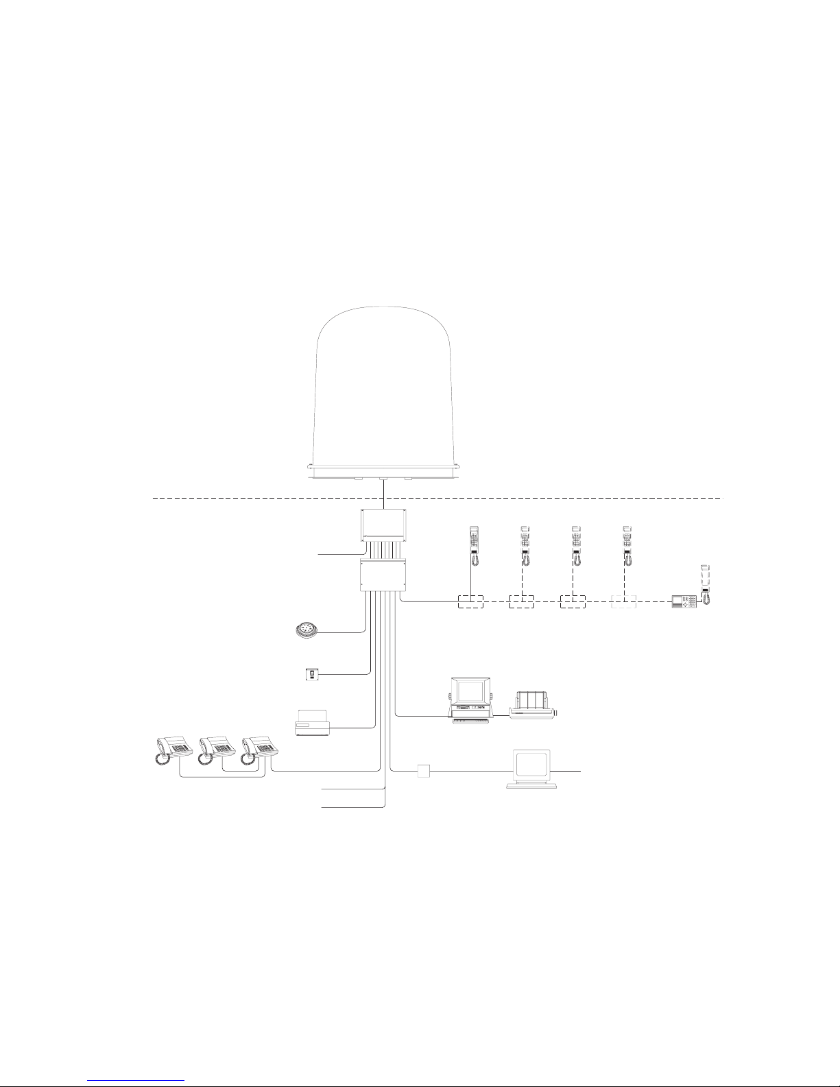
1.1 SYSTEM COMPONENTS
An Inmarsat B terminal can be supplied with various types of service and accessories. The drawing below
shows an installation with the various types of accessories.
ADE: The ADE (Above Deck Equipment) consists of a stabilised platform pointing the
antenna towards the satellite independent of the motion of the ship. Besides the
stabilisation including motors, sensors, tracking and stabilisation processor, the
platform also contains the main part of the RF equipment.
BDE: In the BDE (Below Deck Equipment) are placed the first/last part of the transmitter/
receiver consisting of a baseband UP and DOWN converter. Besides the interface
circuits for the various types of externally connected equipment, the BDE also
contains the signal processing, i.e. error correcting coding/decoding, voice coding/
decoding etc.
Handset: The control handset SC4345 is an integrated handset with display and keyboard used
when a voice call is in progress. A call is set up by entering the phone number from
the handset keyboard. A voice distress call can be started by removing the handset
from the hook and activating the distress button placed in the hook. Another function
of the handset is to use it as a control and set-up unit, where functions like the selection
of coast station and satellite can be carried out.
Control unit: The control unit SC4350 is a desk/bulkhead mounted keyboard and display with an
additional handset without keyboard and display.
Distress button: The distress button can be used to activate a voice or a telex distress alert. The kind
of distress alert the button is used for is selected during installation.
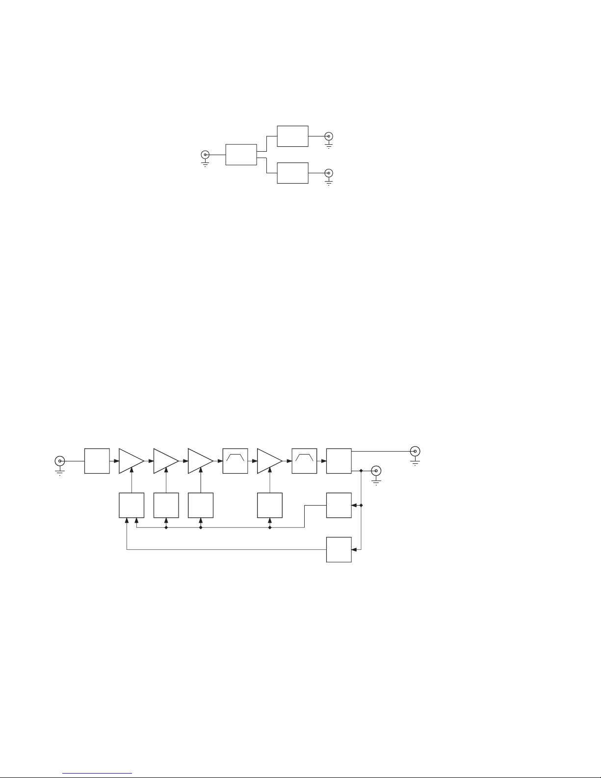
Connection
box: If there is a need for the connection of more than one handset or control unit, the
connection box is used. A maximum of five handsets or control units can be connected
to one transceiver unit which is possible by using four connection boxes.
Veritas: The Veritas connection box can be used as an interconnection box between the
transceiver unit and other system units using ship installation cables. Cables of that
type cannot be connected directly to the relatively small SUB-D connectors at the rear
panel of the transceiver unit.
Inside the Veritas connection box, to interface with ship installation cables, there is a
single printed circuit board containing SUB-D connectors to interface with the
transceiver unit and wire terminal blocks. Besides interfacing between transceiver
unit and ship installations, a gyro repeater is also included. The gyro repeater can be
used if there is no NMEA signal from the gyro of the ship.
Page 10
1 INTRODUCTION Inmarsat B
PAGE 1-3
Inmarsat B
9936
SAT-B TRANSCEIVER
S.P. RADIO DENMARK
PABX Connection or
Push Button Telephone
32213E
Gyro NMEA
GPS NMEA
PABX
Heading Information
56/64 Kbit/sec.
Async./Sync.
Position Information
Personal
Computer
Heading Information
or Gyro
Distress Key
SD4360
Transceiver ST4425 Power Cable DC 24V
Compass
Keyboard
Telex
H1640
Maritime Computer
Connection
H4396
Box
Local Net
Matrix Printer
H1252
Control
Unit
SC4350
ABOVE DECK
BELOW DECK
SC4345
Control Handset
SAT-B Antenna
SA4415
Fascimile (G3)
Veritas
H4394/95
Connection Box
SAT-B Transceiver
ST4425C
can be replaced by Control Unit
All Control Handsets SC4345
SC4350 and vice versa.
Optional
Converter
Hard DiskOn / Off
Page 11

1 INTRODUCTION Inmarsat B
PAGE 1-4
9936
1.2 TECHNICAL DATA
Designation: SAT-B Ship Earth Station (SES) maritime class 1 with area group call capability and
normal tuning range, designed according to Inmarsat B System Definition Manual and
GMDSS requirements.
Configuration: SAT-B antenna SA4415
SAT-B transceiver, 24V ST4425 B/C
Control handset SC4345
Control unit, desk/bulkhead SC4350
Distress key SP4360
Interconnection: SAT-B antenna (ADE) to SAT-B transceiver (BDE):
Single coaxial cable (RG 214) up to 100 m carrying Rx/Tx IF signals (21.4/62.9 MHz),
data (4.8 kbit/s half duplex), 40.32 MHz reference signal and ADE power (40V DC).
SAT-B transceiver (BDE) to control handset and/or control units:
Multiconductor cable (8*0.25 mm2 + screen) up to 300 m implementing Scanbus
interface (LAN 76.8 kbit/s, ISOOSI 1-4), audio (Rx/Tx audio signal, 0 dBm) and power
(24V DC).
Services: Telephony incl. echo cancellation and DTMF signalling (APC vocoder, 16 kbit/s).
Telex (ITA-2, 50 baud).
Data communication (Hayes compatible (AT), 9.6 kbit/s).
Facsimile (CCITT group 3, 9.6 kbit/s).
Optional:
High speed data communication (56/64 kbit/s),
All modes available as duplex and fixed-originated simplex.
External I/F: Scanbus:
(DB-9 connector) Connection of control unit.
NMEA:
(DB-9 connector) Connection of 2-wire NMEA to GPS and GYRO.
DATA: (DB-9 connector) Connection of personal computer.
1 asynchronous serial (high speed) DTE/DCE port (9.6, 56, 64 kbit/s)
according to CCITT Rec. V.11 and X.27.
PC/Printer: (DB-15 connector) Connection of personal computer and printer.
1 asynchronous serial DTE/DCE port (50 baud telex and 9.6 kbit/s data)
according to CCITT Rec.V.24.
1 asynchronous serial DTE/DCE port (printer) according to CCITT Rec.
V24.
Alarm: (DB-15 connector) Connection of alarm unit and alarm indicating unit.
Phone1: (RJ-11 connector) 2W phone/PABX/FAX interface.
Phone2: (RJ-11 connector) 2W phone/PABX/FAX interface.
Antenna: Parabolic dish antenna for RHCP signals (21 dBi gain) with active stabilisation on 3
axes (azimuth, elevation and cross elevation) using rate sensors, inclinometers, and
signal strength tracking.
Transmission: 1626.5 - 1646.5 MHz (normal maritime tuning range, 20 kHz channel spacing for voice
communication).
EIRP = 25, 29, 33 dBW.
Reception: 1525 - 1545 MHz (normal maritime tuning range, 20 kHz channel spacing for voice
communication).
G/T = -4 dB/K.
Modulation: TX 24,132 kbit/s O-QPSK
RX 6 kbit/s BPSK, 24/132 kbit/s O-QPSK.
Coding: FEC convolution coding and 8 level soft decision Viterbi decoding (k = 7) and
(R = 1/2 , 3/4).
For high speed data, a sequential decoder with k = 36 and R = 1/2 is used.
Power Supply: Supply voltage: 24V DC +30/-10%.
Power consumption: TX/RX =250/120W
Environments: SAT-B antenna:
Temperature range: -25 to +55 °C.
SAT-B transceiver:
Temperature range: -15 to +55 °C.
Roll, pitch and yaw: ± 30° (T = 8 s), ± 10° (T = 6 s), ± 8° (T = 50 s)
Turning rate: ± 6 deg/s
Size and weight: SAT-B antenna:
H*W = 1410 mm * 1250 mm
M = 129 kg.
SAT-B transceiver:
H*W*D = 132 mm * 370 mm * 267 mm
M = 8.7 kg
Control handset:
H*L*B = 67 mm * 219 mm ‘ 70 mm
M = 1.2 kg
Control unit:
H*B*D = 100 mm * 200 mm * 120 mm
M = 0.8 kg
Page 12

CONTENTS
2 SYSTEM DESCRIPTION 2-1
2.1 ABOVE DECK EQUIPMENT 2-1
2.1.1 PRINCIPLE OF STABILISATION 2-2
2.1.2 COMPONENTS OF THE STABILISATION SYSTEM 2-3
2.1.3 ANTENNA BEHAVIOUR DURING START-UP SEQUENCE 2-4
2.1.4 ANTENNA BEHAVIOUR DURING GLOBAL SEARCH 2-4
2.1.5 ANTENNA BEHAVIOUR DURING REGION SHIFT SEARCH 2-4
2.1.6 TRACKING ALGORITHM 2-5
2.1.7 COMMUNICATION, SETUP AND STATUS SURVEILLANCE 2-5
2.2 BELOW DECK EQUIPMENT 2-6
9936
Inmarsat B
Page 13
PAGE 2-1
Inmarsat B
9901
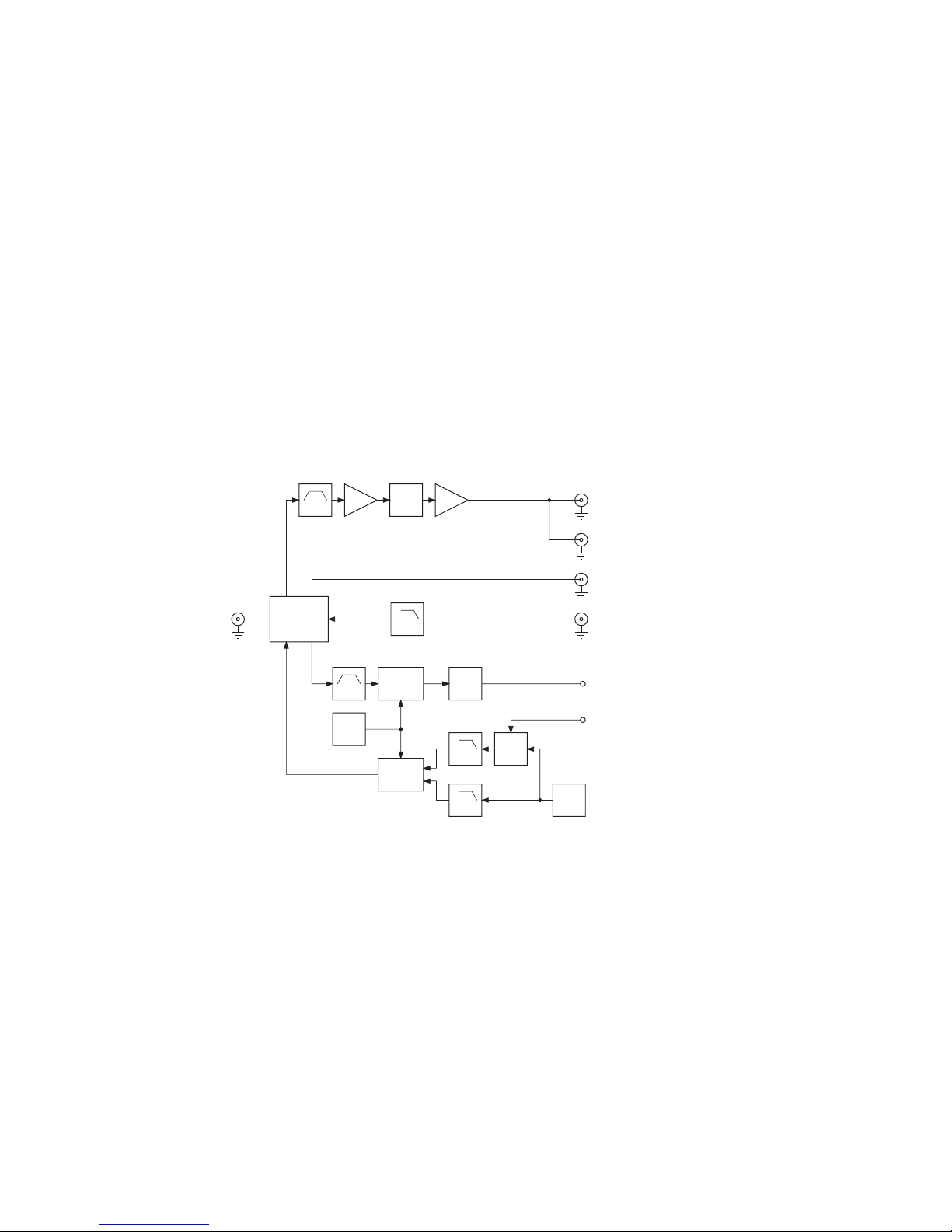
2 SYSTEM DESCRIPTION
The two main parts making up a terminal are described in this chapter. The description of the antenna unit
(ADE) consists of two parts, one concerning the RF and one about the stabilisation. The other main part
of the terminal is the transceiver unit.
2.1 ABOVE DECK EQUIPMENT
The block diagram shown in fig. 2.1 concerns the RF part of the antenna unit.
35522A
Synthesizer
Tracking
Receiver
Converter
Down
Synthesizer
LNA
HPA
Diplexer
Converter
Up
Triplexer Conn. Board
SMPS
Rotary Joint
TSP
Sensor
Block
Motors
DMB
Transmitter Level
Power Control Voltage
Serial Comm. to SMPS
Signal Strength
Data RX/TX
Filter selc.
Frequency Selc.
21.4 MHz RX
10.08 MHz ref.
62.9 MHz TX
DMB
To Transceiver Unit
Fig. 2.1.
The RF part consists of a transmitter and a receiver part sharing a single antenna. The diplexer separates
transmitter and receiver signals to allow full duplex transmission without transmitter degrading receiver
performance.
The transmitter part consists of an UP converter which mixes a fixed intermediate frequency signal to a
signal in the transmitter band (1.6265 - 1.6465 GHz). The frequency selection is made by means of the UP
converter synthesizer. In the HPA (high power amplifier) the low level signal from the UP converter is
amplified before it enters the diplexer and antenna.
The receiver part consists of an LNA (low noise amplifier) and two receiver units, a DOWN converter which
is the counter part of the UP converter, and a tracking receiver which is a part of the tracking and stabilisation
system. The output signal from LNA is split out to both units. The DOWN converter and DOWN converter
synthesizer mix the receiver band (1.525-1.545 GHz) to a fixed intermediate frequency of 21.4 MHz. Due
to different service types, voice, high speed data etc., different receiver bandwidths are required. In the
DOWN converter three bandwidths can be selected on the final intermediate frequency.
The tracking receiver is always tuned to the NCSC channel in a given ocean region. The reason this channel
type is used, is that there is always a signal presented from the satellite, unlike other channel types where
service activation is used. The tracking receiver can be thought of as a frequency selective power meter
which measures the signal level on the channel which it is tuned to. It has its own synthesizer and covers
the entire receiver band. The tracking receiver output is a direct voltage which is used as input for the
tracking and stabilisation system.
As described in the previous chapter, a single coax cable between transceiver unit and antenna unit is used.
To make this concept work, a triplexer is used to distribute the signals from the transceiver unit to the
different modules in the antenna unit and to combine the different signals from the antenna unit to a
composite signal before it enters the cable.
To make the transceiver unit and antenna unit work together, data communication between them is
necessary. On the triplexer board a data receiver/transmitter is placed. The kind of data exchanged between
Page 14

2 SYSTEM DESCRIPTION Inmarsat B
PAGE 2-2
9936
antenna unit and transceiver unit is status and fail information from the antenna and configuration data.
Configuration data concerns frequency set-up of the synthesizer, DOWN converter filter selection, and
transmitter power level. The received data from the transceiver unit is processed by a microcontroller placed
on the tracking and stabilisation processor board, which also takes care of data in the opposite direction.
The tracking and stabilisation processor board is the heart of the antenna stabilisation system. To stabilise
the platform, tilt sensor and rata sensors are placed in different places on the platform. Those sensors
together with the tracking receiver supply input to the tracking and stabilisation processor board, which, as
output, controls the motors. In the following chapter the stabilisation system is described in detail.
The connection from the triplexer to the coax cable is made by means of a connection board and a rotary
joint. The rotary joint is used instead of a cable unwrap system. On the connection board, the main 40V
supply voltage from the transceiver unit is taken out and connected to the input of the switch mode power
supply (SMPS). The SMPS delivers different kinds of supply voltages to the modules. Besides those fixed
voltages, a microprocessor controlled voltage used to regulate the output power from the HPA is also
delivered.
If for some reason signals between transceiver unit and antenna unit are missing, a signal called
dead man’s
button
is activated, shutting the regulated voltage to the HPA, thus preventing the HPA from transmitting.
2.1.1 PRINCIPLE OF STABILISATION
The main objective of the stabilisation system is to keep the antenna pointing as accurately as possible
in the referenced pointing direction at any time under environmental conditions (ship yaw, pitch and roll).
To obtain this the antenna stabilisation system is based on three axis active stabilisation with closed loop
control of each axis. The individual axes are named azimuth (yaw/turning correction), cross elevation and
elevation (roll and pitch correction) as shown in fig. 2.1.1. Each axis uses a double sensor principal for
angular movement measurement (combined measurement of angular rate and absolute angle) and an
electrical motor as actuator. The angular rate is measured by means of angular rate gyros based on
oscillating piezoelectric crystals. For absolute angle reference the elevation (El) and cross elevation (Ce)
axes use a fluid based inclinometer, and the azimuth (Az) axis uses the ships gyro compass.
35972B
Az
Ce
El
Fig. 2.1.1.
Page 15

2 SYSTEM DESCRIPTION Inmarsat B
PAGE 2-3
9936
The controller function of the stabilisation system is performed by the tracking and stabilisation processor
board (TSP board).
In addition to the three axes contributing to the active stabilisation (Az, El and Ce) the antenna is equipped
with a horizontal axis holding a small sensor box. The sensor box holds several of the sensors for the
stabilisation system. Its main function is to make it possible to keep the working point of the inclinometer
sensor as close to the real horizontal level as possible under all antenna elevation reference angles. When
the elevation part of the pointing reference changes, the angle between the antenna disc and the horizontal
box will be changed into the same angle value in the opposite direction, thus keeping the sensor box
horizontal at all times.
2.1.2 COMPONENTS OF THE STABILISATION SYSTEM
Fig. 2.1.2 shows a block diagram of the stabilisation system.
Az rate sensor
El rate sensor
Inclinometer
Tracking receiver
Ce rate censor
Motor Driver
Motor Driver
Motor Driver
Motor Driver
Zero-mark det.
Horizontal
step motor
El axis
step motor
Az axis
step motor
Horizontal axis
DC motor
Brushless
TSP Controller
35973B
Fig. 2.1.2.
The stabilisation system can be divided into functional groups:
Azimuth axis:
Azimuth angular rate gyro sensor.
Fluxgate compass.
Ship gyro.
Azimuth step motor driver.
Azimuth step motor.
Elevation axis:
Elevation angular rate gyro sensor.
Elevation inclinometer (one axis of the dual axis inclinometer unit).
Elevation step motor driver.
Elevation step motor.
Cross elevation:
Cross elevation angular rate gyro sensor.
Cross elevation inclinometer (second axis of the dual axis inclinometer unit)
Cross elevation bldc motor driver.
Cross elevation bldc motor.
Horizontal axis:
Horizontal axis zero mark detector (optical fork).
Horizontal axis step motor driver.
Horizontal axis step motor.
Page 16

2 SYSTEM DESCRIPTION Inmarsat B
PAGE 2-4
9936
2.1.3 ANTENNA BEHAVIOUR DURING START-UP SEQUENCE
When the complete system, or just the ADE, has been reset or switched off and on, the ADE will initialize
and search for the satellite. The behaviour of the antenna during this process is described in this chapter.
1. Initialization
A few seconds after resetting, the horizontal axis will go to the bottom stop position. A knocking
sound will be heard for a few seconds. After this the axis will go up to the optical zero sensor.
Then the elevation axis will initialize in the same manner. Also from this axis a knocking sound
will be heard when it is in the bottom position. When the elevation axis has returned to horizontal
position, the cross-elevation axis will begin to move towards horizontal position. A high-frequency switch-mode sound can be heard when the cross-elevation axis moves. The antenna will
be ready after 2-3 minutes.
If the transceiver has received the position of the vessel, the fast search will begin.
2. Fast search
The elevation axis will move up to the calculated elevation angle of the chosen satellite, and the
azimuth will turn clockwise 360°. This rotation will last about 1-2 minutes. After the search, the
azimuth will go to the position with the highest signal level. This rotation will last less than 1
minute. Here a fine search will be performed.
3. Fine search
The fine search is a cross-shaped search, the centre of which will be in the expected direction of
the satellite. The angular speed of this search is lower than the speed of the fast search. First
the elevation axis will search vertically from 20° below the expected satellite position to 20°
above this position. Then it will search horizontally from 15° to the left of the expected position
to 15° to the right of it. Finally it will move back to the azimuth and elevation angles where the
highest signal levels were measured. The fine search will last 1-2 minutes.
The total start-up sequence will last 5-6 minutes.
2.1.4 ANTENNA BEHAVIOUR DURING GLOBAL SEARCH
If the modem cannot achieve synchronisation on the received NCSC signal within 5 seconds after the fast
search, a global search will start. In this search mode the azimuth will rotate slowly 360° clockwise, and
at the same time the elevation axis will move up and down in a zigzag shape. The elevation top of this zigzag
is 80° above the horizon and the elevation bottom is 5° above the horizon. After this the satellite dish is
turned to the direction where the highest signal level was measured. A ± 25° horizontal and vertical fine
search is performed around the direction whre the highest signal level was measured.
The total global search will last between 6-7 minutes.
2.1.5 ANTENNA BEHAVIOUR DURING REGION SHIFT SEARCH
The behaviour of the antenna during a region shift search depends on whether the position of the vessel
is keyed in manually or received directly from a GPS. In the following description, the values in square
brackets are those of a position keyed in manually, the other values are with a functional GPS connected
to the system.
If for some reason the signal between the satellite system and the ship is blocked by eg. a smokestack
or an other object on board or ashore, it can be necessary to change to an other region. Blocking objects
can cause the signal level to drop to a value where the system is still receiving from the satellite, but where
the quality of the signal is too poor to perform communication. This error may occur if for instance several
calls (Ship to shore) fail, or if only two LEDs are illuminated on the handset. In such cases the transceiver
can be shifted to an other region, in which case a region shift search is performed.
Page 17

2 SYSTEM DESCRIPTION Inmarsat B
PAGE 2-5
9936
When a region shift search is performed, the satellite dish first turns to the direction 15° [45°] to the left (or
right, depending on which is closer) of the expected position of the satellite. From this point it performs a
horizontal search to the point 15° [45°] to the right (or left, if the start position was right) of the satellite. After
this, a ± 15° horizontal and ± 20° vertical fine search is performed around the point where the highest signal
strength was measured. The total region shift search will take 1-2 minutes.
2.1.6 TRACKING ALGORITHM
For long term optimisation of the antenna pointing reference a step-track algorithm is included in the control
system for the antenna. The basic concept of the tracking algorithm is to measure the signal level around
the current centre of pointing by moving the reference in small measurement steps. At each measurement
point the reference position is fixed during an averaging time which is long enough to cover one to several
sea wave periods. After the averaging period the mean level is interpreted as the tracking level for that
reference point. This measurement is repeated several times at equally spaced points on each side of the
centre point before a decision is taken in which direction to move the centre. This procedure is repeated
on the elevation and azimuth axes one at a time until a new search is started. The size of the measurement
steps on the azimuth axis increases when the elevation reference angle increases.
2.1.7 COMMUNICATION, SETUP AND STATUS SURVEILLANCE
In addition to antenna tracking and stabilisation the TSP controller works as the central control unit in the
ADE and takes care of various setup and control tasks in the ADE.
Control data communication with the BDE:
Receiver, transmitter and tracking receiver channels.
Search initiation and sky slice parameters.
Ship gyro compass information.
Transmitter power level.
Antenna status information.
HPA setup and error reporting:
The TSP communicates with the microcontroller in the HPA unit. Power level information, burst length information and transmitter frequency range are sent to the HPA.
Status information and error codes are received from the HPA and reflected to the BDE
whenever needed.
Synthesizer setup:
The three synthesizer groups in the antenna (up converter, down converter and tracking
receiver) are all programmed by the TSP with configuration and frequency information.
The frequency programming parameters are calculated by the TSP based on the
channel numbers received from the BDE. In addition the TSP surveys the lock signals
generated by the synthesizers to detect if a synthesizer is unlocked. Unexpected
unlock situations are reported to the BDE.
Page 18
2 SYSTEM DESCRIPTION Inmarsat B
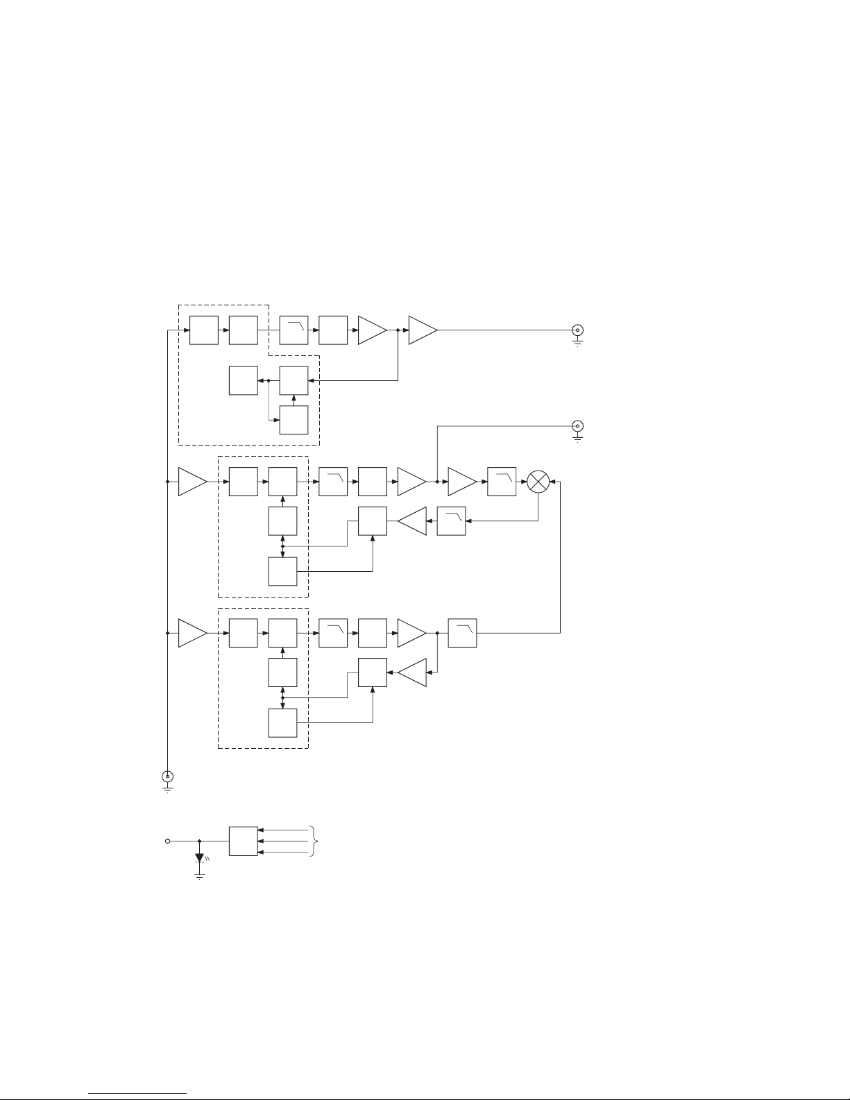
2.2 BELOW DECK EQUIPMENT
The below deck equipment or transceiver unit as it is called consists of five printed circuit boards (modules)
as shown in fig. 2.3.
Pax
CSP/VDP
Modem
SPS
Rear Panel Connectors
SMI
SMPS
35974
Fig. 2.3.
SPS board
The SPS (signal path and synthesizer) board is the interface between the analogue RF parts at the antenna
unit and the digital signal processing in the transceiver unit. The receiver IF of 21.4 MHz is converted to
baseband, sampled and processed in a digital signal processor.
The transmitter part consists of a quadrature mixer where two baseband data signals are up converted and
combined to a 62.9 MHz IF signal. The baseband signals are generated in the modem module.
A data receiver and transmitter for communication with the antenna unit is also placed at this board.
All critical frequencies are derived from the system reference oscillator. The oscillator is a crystal oscillator
built into an oven.
The RF input/output to/from the SPS board is a single coax connection. Therefore, a combiner/splitter
circuit is used to combine the RF signals to be sent to the antenna unit and the split-out received RF signal
to the respective blocks which are to use them.
Modem board
The purpose of the modem board is to code data flow sent from the terminal to the satellite and decode data
flow received from the satellite. Coding is used to make it possible to detect and correct bit errors, thus
increasing the quality of the communication.
To increase the security, data bits are scrambled. Scrambling and descrambling takes place in the modem.
Data flow is transmitted/received in frames. The contents of a frame, besides the data to be transmitted
or received, are bit sequences helping the modem to synchronise. The modem takes care of the frame
format in both the receiver and the transmitter directions.
CSP/VDP board
The CSP/VDP board consists of two functionally separate parts. The CSP (control and signalling processor)
is the main processor in the system and takes care of the satellite protocol, man/machine and external
equipment interfaces.
The VDP (voice and data processor) is a digital signal processor which handles voice coding and decoding
and is the interface between modem and the PAX module for data and fax services.
PAGE 2-6
9936
Page 19

2 SYSTEM DESCRIPTION Inmarsat B
PAGE 2-7
9936
PAX board
The PAX board (phone and fax) contains hardware and software for interfacing with a fax machine and with
push button telephones like a stand-alone telephone or a PABX network.
The module also acts as an interface for data communication from a single terminal or a local network at
transmission rates of 9.6 or 64 kbit/s (64 kbit/s only possible if high speed data is implemented).
SMI board
The SMI (switch mode power supply and interconnection) board contains the system power supply. From
the ship, the main supply voltage of 24V DC is connected at the rear panel of the transceiver unit. And from
that, the switch mode power supply generates a number of different voltages not only for the modules in
the transceiver unit but also 40V DC for the antenna unit.
At the rear panel of the transceiver unit, a number of connectors are placed for externally connected
equipment. Those connectors are mounted on the board, from where they are connected to the respective
modules by means of ribbon cables.
Page 20

CONTENTS
3 MODULE DESCRIPTION 3-1
3.1 ABOVE DECK EQUIPMENT 3-1
3.1.1 ANTENNA 3-1
3.1.2 DIPLEXER 3-2
3.1.3 LNA 3-2
3.1.4 DOWN CONVERTER 3-3
3.1.5 UP CONVERTER 3-4
3.1.6 HPA 3-4
3.1.7 TRACKING RECEIVER 3-5
3.1.8 TRIPLEXER 3-6
3.1.9 SYNTHESIZER FOR TRACKING RECEIVER 3-8
3.1.10 SYNTHESIZER FOR UP/DOWN CONVERTER 3-10
3.1.11 SWITCH MODE POWER SUPPLY 3-13
3.1.12 TSP 3-14
3.1.13 TILT SENSOR 3-15
3.2 BELOW DECK EQUIPMENT 3-16
3.2.1 SPS BOARD 3-16
3.2.2 MODEM BOARD 3-18
3.2.3 CSP/VDP BOARD 3-19
3.2.4 PAX BOARD 3-20
3.2.5 SMI BOARD 3-21
3.2.6 HANDSET 3-22
9936
Inmarsat B
Page 21
PAGE 3-1
9849
3 MODULE DESCRIPTION
This chapter contains a description of the modules making up an Inmarsat B terminal, including modules
placed at the antenna unit and transceiver unit.
3.1 ABOVE DECK EQUIPMENT
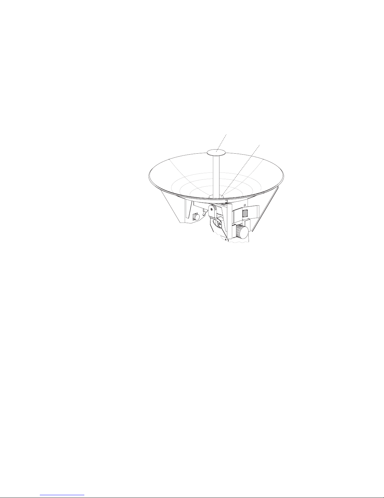
3.1.1 ANTENNA
The antenna is a parabolic dish antenna as shown in fig. 3.1.
35971
SMA connector
Sub reflector
Fig. 3.1.
The diameter of the parabolic reflector is 90 cm and the feeder element is placed inside the plastic tube
in the focal point of the reflector. A small reflector with a diameter of 12 cm is placed at the end of the plastic
tube. The feeder element is a helical antenna operating in axial mode, thus creating a wave of circular
polarisation as required from Inmarsat. The wave is right handed. The helix is wrapped around a form of
polystyrene.
Inside the tube, a semi rigid coax cable connects the feeder element with the SMA connector at the bottom
of the parabolic reflector. This connector is connected to the diplexer through a highly flexible coax cable.
The following is a list of the most important antenna specifications:
Antenna gain: 20.9 dBi
Polarisation: Right handed circular
3 dB beam width: ± 7.5°
Side lobe level: More than 20 dB below main lobe
Axial ratio: Better than 2 dB
Inmarsat B
Page 22
3 MODULE DESCRIPTION Inmarsat B
PAGE 3-2
9901
3.1.2 DIPLEXER
When a conversation is in progress via a satellite, the transmission mode is normally duplex which means
that the transmitter and receiver are active simultaneously. To prevent the HPA from overloading the LNA,
an interconnection device is used, i.e. a diplexer. Fig. 3.2 shows a block diagram of the diplexer.
Network
Coupling
TX Filter
Antenna Port
TX Port
RX Filter RX Port
35523A
Fig. 3.2.
The diplexer is a mechanical device, built up as two tenth-order band-pass filters connected to a coupling
network at the antenna port. The receiver path pass band is 1525 to 1545 MHz, and the transmitter path
pass band is 1626.5 to 1646.5 MHz.
Each filter is constructed of quarterwave resonators, the distance between them determining the coupling
coefficient. The tuning capacitors are made using screws in the top cover of the diplexer. Changing the
distance between a tuning screw and the resonator causes the top loading capacity to change, thus
changing the resonance frequency of the resonator as well.
The resonators are made of aluminium rods and the whole unit is silver plated to obtain a low insertion
loss. Furthermore, the device is sealed on the outside to avoid oxidation.
To obtain a low receiver noise figure, the LNA is placed in the diplexer. Interconnection between diplexer
receiver port and LNA input is made by means of a short piece of semi rigid cable. At antenna and TX
port, SMA connectors are used.
3.1.3 LNA
The main signal path in the LNA is constructed with four transistors and two helical filters as shown in
fig. 3.3.
Network
Matching
Down Converter
Tracking Receiver
1535 MHz 1535 MHz
Power
Divider
Bias Bias Bias Bias
Reg.
Voltage
Reg.
Voltage
BjtBjt BjtGaAs
35524
Fig. 3.3.
The semi rigid cable from the diplexer is soldered directly to the printed circuit board where it is connected
to a microstrip impedance matching network. The matching network acts as interconnection between
diplexer and the first gain stage to obtain a low noise figure. The first amplifier stage consists of a low noise
GaAs FET whereas the remaining three stages are based on junction transistors.
The two helical filters cover the maritime band, 1525 to 1545 MHz and ensure high immunity for out of
band signals. After the last filter, a microstrip power divider equally divides the signal to tracking receiver
and DOWN converter inputs.
The LNA is supplied with +18V DC from the tracking receiver through the coax cable which also carries
the RF signal.
In order to minimise gain variation over the entire temperature range, active bias network is used to keep
the current in each stage constant. The GaAs FET also uses a negative bias voltage which is made from
the +18V supply in a DC to DC converter based on pulse width modulation.
Page 23
3 MODULE DESCRIPTION Inmarsat B
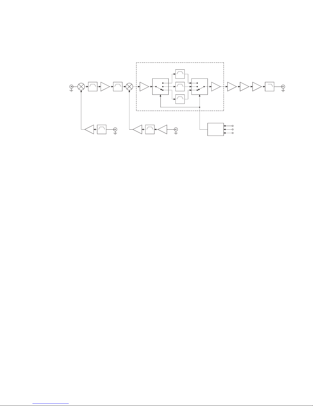
3.1.4 DOWN CONVERTER
The purpose of the DOWN converter is to convert an L-band signal to a fixed intermediate frequency of
21.4 MHz. A block diagram is shown in fig. 3.4.
20 kHz
10 kHz
100 kHz
Filter Module
Shift
Register
21.4 MHz
Data
Clock
Strobe
Lo-1 Lo-2
35525
Fig. 3.4
Down conversion takes place in two steps. The L-band signal is mixed to a first intermediate frequency
of 179.32 to 179.6325 MHz. The first IF signal is then mixed to 21.4 MHz. The reason why the first IF is
not fixed is that the frequency of the L-band synthesizer steps in 315 kHz. This is done to lower the close
in phase noise.
From the output of the LNA, the received signal is fed directly to RF input of the first mixer. The mixer is
a passive doubled balanced diode mixer with good large-signal properties. The local oscillator frequency
ranges from 1345.68 to 1365.525 MHz. The signal level from the synthesizer module is 0 dBm ± 3 dB and
is amplified in a MMIC to the required LO drive level of 10 dBm. To avoid power level variation of the local
oscillator input of the mixer, the compression point of the amplifier is approximately 10 dBm. Before
amplification takes place, the signal is filtered. The purpose of this filter is to attenuate spurious
frequencies which may add to the synthesizer module oscillator signal.
The first intermediate frequency consists of two double tuned band-pass filters separated by a dual gate
MOS-FET amplifier. The total power gain including filter losses is approximately 8 dB. The power gain
is temperature compensated by means of an NTC resistor in the bias network of the MOS-FET transistor.
The final down conversion to second IF at 21.4 MHz takes place in the second. This mixer has the same
properties as the first one. The second local oscillator amplifier amplifies the synthesizer signal from
-20 dBm to the required level of 10 dBm. The amplifier is built up as a two stage tuned transistor amplifier
with a 3 dB attenuator separating the transistors. The selectivity is formed by the tuned impedance
matching networks. This amplifier also has a compression point of approximately 10 dBm.
Due to the different types of services (voice, high speed data, telex etc.) different receiver bandwidths are
required. In the DOWN converter it is possible to select between three different crystal filters, i.e. 10, 20
and 100 kHz. Those filters are located on another PCB together with buffer stages and filter selection
circuits. The filter selection is made by means of switch diodes which are controlled by a TTL shift register.
Three control signals (data, clock and strobe) to set up the shift register are supplied from the TSP board.
The filter module buffer stages have two purposes, to amplify the signal and to serve as interconnection
between the filter module and the main board.
Finally the signal is amplified in a two stage dual gate MOS-FET amplifier, and a common collector stage
takes care of the impedance matching to a 50 ohm load.
All internal supply voltages (+15, -12 and 5V) are made by means of integrated voltage regulators.
PAGE 3-3
9901
Page 24
3 MODULE DESCRIPTION Inmarsat B
3.1.5 UP CONVERTER
The input signal to the UP converter is mixed in two steps to cover the frequency band from 1626.5 to
1646.5 MHz.
Lo-1 Lo-2
Output to HPAInput from Triplexer
62.9 MHz
ATT
150 MHz 150 MHz
ATT
1636.5
35526
Fig. 3.5.
The input signal to the UP converter is filtered to attenuate out-of-band signals before the first frequency
conversion. Between the filter and first mixer, a 3 dB attenuator is used to improve termination. The mixer
is a passive double balanced diode mixer. Second IF is at 150.1 to 150.415 MHz. Second IF is built up
as band-pass filter, a BJT amplifier, another band-pass filter and finally an attenuator. The amplifier is
temperature compensated to minimise gain variations and includes a gain adjustment to set up the overall
gain of the UP converter. The final frequency conversion to L-band takes place in the second mixer. The
RF signal at the output of the mixer is filtered with a helical filter to reduce out-of-band spurious. The final
amplification takes place in an MMIC.
The two local oscillator signals are delivered by the UP converter synthesizer. The frequency of the first
LO is 213.0025 to 213.315 MHz. To obtain the required drive level of 7 dBm to the mixer LO port is used
a buffer built up with two transistors. The last stage is driven into compression to maintain a constant
power level to the mixer. To minimise intermodulation products, a bandpass filter between the two
transistors attenuates unwanted signals.
The frequency range of the second local oscillator is 1776.915 to 1810.620 MHz. The buffer stage
consists of a bandpass filter and an MMIC which is also driven into compression at a power level of 7 dBm.
All internal supply voltages are +15V DC and generated by means of integrated voltage regulators.
3.1.6 HPA
When mounted in the ADE, the HPA is placed in a separate, enclosed cabinet. The block diagram in
fig. 3.6 shows the main parts of the HPA.
Power Module
M Controller
DMB
1635.5 1635.5
Power
Det.
Senser
Temp.
EE-Prom
Clock
Data
Strobe
Clock
Data
Strobe
Data
+28V DC
SMPS
TSP
Input from
UP Converter
Output to
Diplexer
Directional
Coupler
35527
Fig. 3.6.
PAGE 3-4
9901
Page 25
3 MODULE DESCRIPTION Inmarsat B
PAGE 3-5
9901
To reject out of band signals, a helical filter is placed at the input of the HPA. The output signal from the
UP converter can vary approximately 17 dB depending on the length of the cable between BDE and ABE,
temperature variations and AM fluctuations in the different digital modulation forms used. To remove
variations in the signal power, the signal is amplified in a two-stage amplifier built up around two integrated
amplifiers. The amplifiers are driven into compression, thus removing the power variation. A second
helical filter is located after the amplifier stages to attenuate the harmonic contents of the signal.
The final amplification is performed in the power amplifier, which is an integrated amplifier. The output
power can be controlled by varying the +28VR DC supply voltage to the power amplifier. The power
regulation facility serves two purposes: transmission at three predefined power levels and correction of
each power level due to temperature variations and parameter spread of the components.
From the directional coupler at the output of the HPA, a small part of the transmitter signal is taken out,
and a power detector built up around a Schottky diode converts the signal to a direct voltage which is
proportional to the transmitter power. The DC voltage is sampled by means of an A/D converter inside
the microcontroller.
A circulator at the output of the directional coupler is used to protect the power module if for some reason
the transmitter power is reflected back into the power module.
A sensor monitors the instantaneous temperature of the module, and its output is connected to a
microcontroller.
The microcontroller is connected to an A/D converter in the switch mode power supply which regulates
the +28VR DC and thus the transmitter power. If for some reason a burst in burst mode transmission
becomes too long, the output power or the temperature becomes too high, the microcontroller forces the
switch mode power supply to shut down the +28VR DC supply voltage and thus the transmitter power.
The interconnection between the microcontroller and the switch mode power supply is a serial
connection.
If a fail condition arises, an error code is transmitted to the TSP board, from where it is sent to the system
processor in the transceiver unit.
During a call, the TSP receives information concerning transmission, i.e. burst or continues mode and
power level. That information is given to the microcontroller in the HPA, from where the A/D converter in
the SMPS is controlled.
3.1.7 TRACKING RECEIVER
The tracking receiver can be considered as an ordinary receiver whose detector delivers a direct voltage
proportional to the received signal level.
The input signal to the tracking receiver is taken from a power divider located at the LNA. The coax cable
between LNA and the tracking receiver is also used to supply the LNA with DC power. In fig. 3.7 a block
diagram is shown.
Lo-1
To TSP
134 MHz 134 MHz
6 dB
Lo-2
10.7 MHz
ATT
10.7 MHz
DC
IF1 IF2
AGC
Level
Converter
35528
Fig. 3.7.
The receiver is built up as a double conversion receiver, with a first IF of 133.96 to 134.27 MHz. The
second IF is fixed at 10.7 MHz. The reason why the first IF is not fixed is that the frequency of the L-band
synthesizer is changed in step of 315 kHz. This is done in order to lower close in phase noise.
The DC block between tracking receiver input and first mixer adds an 18V supply voltage to the coax cable
up to the LNA and makes sure that the DC voltage does not reach the mixer input.
The first mixer, a double balanced diode mixer, down converts the L-band signal to first IF where two
double tuned bandpass filters separated by a dual gate MOS-FET amplifier reject image frequencies. The
final down conversion to 10.7 MHz is made by means of a mixer of the same type as the first one. At second
Page 26
3 MODULE DESCRIPTION Inmarsat B
PAGE 3-6
9901
IF, adjacent channel selectivity is obtained in a crystal filter. Between the mixer and crystal filter, a 6 dB
attenuator is used to improve the termination impedance of the mixer IF port.
Second IF consists of two integrated amplifiers of which the first has fixed and the second variable gain
controlled by a DC voltage. After that a crystal filter limits the noise bandwidth before the final amplification
in a two-stage transistor amplifier.
A diode detector converts the IF signal to a DC voltage proportional to the signal strength. An AGC circuit
ensures that the detector voltage is constant by regulating the gain of the second IF2 amplifier. The
voltage regulating the gain is used as an indicator of the signal strength. When the input power for the
tracking receiver changes from minimum to maximum, the AGC voltages change by approximately 0.5V.
A level converter is used to give a 0-5V change for the same input power variation. This signal is connected
to the TSP board.
The module uses +15 and -12V supply voltages generated by integrated voltage regulators.
3.1.8 TRIPLEXER
The main function of the triplexer is to combine and distribute signals in the coax cable between ADE and
BDE to and from the different modules placed on the antenna unit. A block diagram of the triplexer is
shown in fig. 3.8.
:4
40.32 MHz
21.4 MHz
87 MHz
Circuit
FM-IF
Slicer
Data
OSC.
99 MHz
Vector
Modulator
150 kHz
150 kHz
Phase
Control
OSC.
150 kHz
Combiner
Splitter/
Converter Synthesizer
10.08 MHz to UP/Down
10.08 MHz to Tracking
Receiver Synthesizer
62.9 MHz output to
UP Converter
21.4 MHz input
from Down Converter
Data to TSP
Data from TSP
To Connection Board
35529
Fig. 3.8.
The input block consists of a number of baluns separating the different types of signals from the BDE and
combining the signals to the BDE. The different types of signal are listed below:
40.32 MHz reference signal
In the BDE is placed a stable oscillator which is used to derive the reference frequencies for the
synthesizers, among other things. The oscillator frequency is 10.08 MHz but is multiplied by a factor four
before entering the coax cable. This signal is taken out of the combiner/splitter block and filtered in a
bandpass filter with a center frequency of 40.32 MHz. The signal amplification takes place in an integrated
circuit and two discrete transistors. The last transistor is a switch transistor converting the signal to a level
suitable for TTL circuits. After level conversion, the frequency is divided by a factor four to obtain the
original reference frequency of 10.08 MHz. The divider circuits are built up around two d-type flip-flops.
The 10.08 MHz signal is now amplified and finally split out to two SMB connectors. From those
connectors, the reference frequencies for the tracking receiver and UP/DOWN converter synthesizer are
taken.
Page 27

3 MODULE DESCRIPTION Inmarsat B
PAGE 3-7
9905
62.9 MHz UP converter signal
The transmitter signal from the BDE, which is a 62.9 MHz intermediate frequency signal, is taken out of
the combiner/splitter block and is fed directly to an SMB connector where the input of the UP converter
is connected.
21.4 MHz DOWN converter signal
The output signal from the DOWN converter enters the triplexer board in an SMB connector and is then
low-pass filtered before entering the combiner/splitter block.
Data receiver/transmitter
As described in the previous chapter, data communication between ADE and BDE is necessary. On the
triplexer board, a complete 4800 bit/s data receiver /transmitter is placed. The data receiver/transmitter
is built up as an FSK (frequency shift key) modem where a 99 MHz transmitter carrier is shifted ± 150 kHz
in frequency depending on the data bit (one or zero). The receiver is based on the same principle except
that the centre frequency is 87 MHz. The data receiver is built up around an integrated circuit which is
a complete FM IF subsystem. The integrated circuit contains a mixer which converts the 87 MHz receiver
signal to an intermediate frequency of 12 MHz. The needed local oscillator signal is taken from the 99 MHz
crystal oscillator. The 12 MHz FSK modulated IF signal is demodulated in an frequency discriminator.
After demodulation the signal is led to a data slicer reconstituting the data shape. The serial bit stream
from the data slicer is connected to the TSP board. The data transmitter is built up around an integrated
vector modulator. The modulation is generated through a 150 kHz I/Q signal, the phase of the Q signal
switched 0 or 180° depending on the I signal controlled by the bit stream to be transmitted. The I and Q
signals are square waves, but low-pass filters attenuate the harmonic contents to generate low distortion
sine and cosine signals as vector modulator input.
Page 28
3 MODULE DESCRIPTION Inmarsat B
PAGE 3-8
9901
3.1.9 SYNTHESIZER FOR TRACKING RECEIVER
The two local oscillator signals used in the tracking receiver are generated on this synthesizer module.
The first local oscillator which is used to mix the receiver frequency to first IF is called L-band synthesizer
and the other is called VHF synthesizer.
The frequency coverage of the two synthesizers is listed below:
L-band synthesizer: 1391.040 - 1410.885 MHz in steps of 315 kHz
VHF synthesizer: 144.66000 - 144.97375 MHz in steps of 1.25 kHz
A block diagram of the synthesizer module is shown in fig. 3.9.
LOOP 1
PD:32 VCO
:N :64/65
:A
PD:126 VCO
:N
:A
:20/21
:A
:N :20/21
:128 PD VCO
VHF
L Band
Lock
det.
LOOP 2
10.08 MHz
from Triplexer
To TSP
from PLL
Lock Signals
35530
Fig. 3.9.
L-band synthesizer
The L-band oscillator is based on a voltage controlled oscillator (VCO) with good close-in phase noise
properties. Frequency stability is obtained using a PLL circuit where the VCO is locked to the highly stable
reference frequency supplied from the triplexer board.
Page 29

3 MODULE DESCRIPTION Inmarsat B
PAGE 3-9
9901
The integrated PLL circuit contains phase detector, divider for reference frequency, divider with modulus
two architecture and built in L-band prescaler with a division ratio of 64/65.
The 10.08 MHz reference frequency is divided by 32 in the reference divider to obtain a frequency
resolution of 315 kHz.
The loop filter is an active low-pass filter built up around a low noise operational amplifier. The output
signal from the VCO is amplified in two integrated L-band amplifiers (MMIC). The purpose of the amplifiers
is not only to obtain the required signal level but also to isolate the frequency determining components
in the VCO from the rest of the circuits.
VHF synthesizer
The VHF synthesizer is also based on PLL technology but because of the high frequency resolution of
1.25 kHz and demands for low phase noise, a dual loop synthesizer is used. The two loops are built up
as conventional synthesizers with the exception that loop 1 contains a mixer.
The reference divider in loop 1 is 126, giving a frequency resolution of 80 kHz, and for loop 2 it is 128,
giving a frequency resolution of 78.75 kHz.
When the divider in the feed back loop of loop 1 is incremented by 1, the output frequency of the VHF
synthesizer is increased by 80 kHz. If at the same time, the divider in the feed back loop of loop 2 is reduced
by one, the output frequency of the VHF synthesizer is decreased by 78.75 kHz. The resulting change
of frequency at the output of the VHF synthesizer is therefore only 1.25 kHz.
The integrated PLL circuits used in loop 1 and 2 do not include the prescaler. Therefore, external
prescalers with a division ratio of 21/22 are used. The loop filters are of same type as the one used in the
L-band synthesizer.
The VCO’s are a Colpitts-Clapp type, built up with BJT’s . Before the amplified VCO signals enter the loop
mixer, they are low-pass filtered to attenuate the harmonic contents. Loop mixing takes place in a passive
double balanced diode mixer, and at the output the mixer, a low-pass filter removes the sum frequency.
For initialization and selection of frequencies, the PLL circuits need three signals each: clock, data and
strobe. The strobe signal is used for chip selection and therefore three separate wires are used. The clock
and data signals are the same for the three PLL’s, the strobe signals determining which one is loaded with
data. The strobe, data and clock signals are generated from the TSP board.
Each of the three PLL’s has a built in lock detector which indicates when a VCO is unlocked. These signals
are combined in a lock indicator circuit which indicates if one or more VCO’s are unlocked. The lock
condition is signalled to the TSP board, which sends this information to the transceiver unit. The lock
indicator is also connected to a led placed on the synthesizer board, which is lit when a VCO is unlocked.
The supply voltages (+18V, +8V, -15.5V) from the SMPS are converted to +15V, +5V and -1.25V by
standard voltage regulators but the more critical supply voltages to VCO’s and phase detectors are made
by discrete components to lower the noise level.
Page 30
3 MODULE DESCRIPTION Inmarsat B
PAGE 3-10
9901
3.1.10 SYNTHESIZER FOR UP/DOWN CONVERTER
The UP and DOWN converter synthesizers are two separate units but placed on the same printed circuit
board.
UP converter synthesizer
The two local oscillator signals used in the UP converter are generated on this synthesizer module. The
first local oscillator which is used to mix the transmitter frequency to first IF is named VHF synthesizer
and the other is named L-band synthesizer.
The frequency coverage of the two synthesizers are listed below:
L-band synthesizer: 1776.915 - 1810.620 MHz in steps of 315 kHz
VHF synthesizer: 213.0025 - 213.3150 MHz in steps of 2.5 kHz
A block diagram of the UP converter synthesizer is shown in fig. 3.10.
LOOP 1
PD:32 VCO
:N :64/65
:A
PD:63 VCO
:N
:A
:20/21
:A
:N :20/21
:64 PD VCO
VHF
L Band
Lock
det.
LOOP 2
10.08 MHz
from Triplexer
To TSP
from PLL
Lock Signals
35534
Fig. 3.10.
Page 31

3 MODULE DESCRIPTION Inmarsat B
PAGE 3-11
9901
L-band synthesizer
The L-band oscillator is based on a voltage controlled oscillator (VCO) with good close in phase noise
properties. Frequency stability is obtained using a PLL circuit, the VCO locked to the highly stable
reference frequency supplied from the triplexer board.
The integrated PLL circuit contains phase detector, divider for reference frequency, divider with modulus
two architecture and built in L-band prescaler with a division ratio of 64/65.
The 10.08 MHz reference frequency is divided by 32 in the reference divider to obtain a frequency
resolution of 315 kHz.
The loop filter is an active low-pass filter built up around a low noise operational amplifier. The output
signal from the VCO is amplified in two integrated L-band amplifiers (MMIC). The purpose of the amplifiers
is not only to obtain the required signal level but also to isolate the frequency determining components
in the VCO from the rest of the circuits.
VHF synthesizer
The VHF synthesizer is also based on PLL technology but because of the high frequency resolution of
2.5 kHz and demands for low phase noise, a dual loop synthesizer is used. The two loops are built up as
conventional synthesizers with the exception that loop 1 contains a mixer.
The reference divider in loop 1 is 63 giving a frequency resolution of 160 kHz and for loop 2 it is 64, giving
a frequency resolution of 157.5 kHz.
When the divider in the feed back loop of loop 1 is incremented by 1, the output frequency of the VHF
synthesizer is increased by 160 kHz. If at the same time, the divider in the feed back loop of loop 2 is
reduced by one, the output frequency of the VHF synthesizer is decreased by 157.5 kHz. The resulting
change of frequency at the output of the VHF synthesizer is therefore only 2.5 kHz.
The integrated PLL circuits used in loop 1 and 2 do not include the prescaler. Therefore, external
prescalers with a division ratio of 21/22 are used. The loop filters are of same type as the one used in the
L-band synthesizer.
The VCO’s are a Colpitts-Clapp type, built up with BJT’s . Before the amplified VCO signals enter the loop
mixer, they are low-pass filtered to attenuate the harmonic contents. Loop mixing takes place in a passive
double balanced diode mixer, and at the mixer output, a low-pass filter removes the sum frequency.
For initialisation and selection of frequencies, the PLL circuits need three signals each: clock, data and
strobe. The strobe signal is used for chip selection, and therefore three separate wires are used. The clock
and data signals are the same for the three PLL’s, the strobe signals determining which one is loaded with
data. The strobe, data and clock signals are generated from the TSP board.
Each of the three PLL’s has a built-in lock detector indicating when a VCO is unlocked. These signals are
combined in a lock indicator circuit indicating if one or more VCO’s are unlocked. The lock condition is
signalled to the TSP board, which sends this information to the transceiver unit. The lock indicator is also
connected to a led, placed on the synthesizer board, which is lit when a VCO is unlocked.
The supply voltages ( +18V, +8V, -15.5V) from the SMPS are converted to +15V, +5V and -1.25V by
standard voltage regulators, but the more critical supply voltages to VCO’s and phase detectors are made
by discrete components to lower the noise level.
DOWN converter synthesizer
The two local oscillator signals used in the DOWN converter are generated on this synthesizer module.
The first local oscillator which is used to mix the receiver frequency to first IF is called L-band synthesizer
and the other is called VHF synthesizer.
The frequency coverage of the two synthesizers is listed below:
L-band synthesizer: 1345.680 - 1379.385 MHz in steps of 315 kHz
VHF synthesizer: 200.7200 - 201.0325 MHz in steps of 2.5 kHz
A block diagram of the synthesizer module is shown in fig. 3.11.
Page 32

3 MODULE DESCRIPTION Inmarsat B
PAGE 3-12
9901
LOOP 1
PD:32 VCO
:N :64/65
:A
PD:63 VCO
:N
:A
:20/21
:A
:N :20/21
:64 PD VCO
VHF
L Band
Lock
det.
LOOP 2
10.08 MHz
from Triplexer
To TSP
from PLL
Lock Signals
35534
Fig. 3.11.
L-band synthesizer
The L-band oscillator is based on a voltage controlled oscillator (VCO) with good close in phase noise
properties. Frequency stability is obtained using a PLL circuit, the VCO locked to the highly stable
reference frequency supplied from the triplexer board.
The integrated PLL circuit contains phase detector, divider for reference frequency, divider with modulus
two architecture and built in L-band prescaler with a division ratio of 64/65.
The 10.08 MHz reference frequency is divided by 32 in the reference divider to obtain a frequency
resolution of 315 kHz.
The loop filter is an active low-pass filter built up around a low noise operational amplifier. The output
signal from the VCO is amplified in two integrated L-band amplifiers (MMIC). The purpose of the amplifiers
is not only to obtain the required signal level but also to isolate the frequency determining components
in the VCO from the rest of the circuits.
VHF synthesizer
The VHF synthesizer is also based on PLL technology but because of the high frequency resolution of
2.5 kHz and demands for low phase noise, a dual loop synthesizer is used. The two loops are built up as
conventional synthesizers with the exception that loop 1 contains a mixer.
The reference divider in loop 1 is 63, giving a frequency resolution of 160 kHz, and for loop 2 it is 64, giving
a frequency resolution of 157.5 kHz.
When the divider in the feed back loop of loop 1 is incremented by 1, the output frequency of the VHF
synthesizer is increased by 160 kHz. If at the same time, the divider in the feed back loop of loop 2 is
reduced by one, the output frequency of the VHF synthesizer is decreased by 157.5 kHz. The resulting
change of frequency at the output of the VHF synthesizer is therefore only 2.5 kHz.
Page 33

3 MODULE DESCRIPTION Inmarsat B
The integrated PLL circuits used in loop 1 and 2 do not include the prescaler. Therefore, external
prescalers with a division ratio of 21/22 are used. The loop filters are of same type as the one used in the
L-band synthesizer.
The VCO’s are a Colpitts-Clapp type, built up with BJT’s . Before the amplified VCO signals enter the loop
mixer, they are low-pass filtered to attenuate the harmonic contents. Loop mixing takes place in a passive
double balanced diode mixer, and at the output the mixer, a low-pass filter removes the sum frequency.
For initialisation and selection of frequencies, the PLL circuits need three signals each: clock, data and
strobe. The strobe signal is used for chip selection and therefore three separate wires are used. The clock
and data signals are the same for the three PLL’s, the strobe signals determining which one is loaded with
data. The strobe, data and clock signals are generated from the TSP board.
Each of the three PLL’s has a built-in lock detector indicating when a VCO is unlocked. These signals are
combined in a lock indicator circuit indicating if one or more VCO’s are unlocked. The lock condition is
signalled to the TSP board, which sends this information to the transceiver unit. The lock indicator is also
connected to a led, placed on the synthesizer board, which is lit when a VCO is unlocked.
The supply voltages ( +18V, +8V, -15.5V) from the SMPS are converted to +15V, +5V and -1.25V are
generated by standard voltage regulators, but the more critical supply voltages to VCO’s and phase
detectors are made by discrete components to lower the noise level.
3.1.11 SWITCH MODE POWER SUPPLY
The 40V DC supplied from the transceiver unit is converted to different voltage levels needed to supply
the modules and motors. This is done in the switch mode power supply. Actually the power supply consists
of two power units based on switch mode technology. The two switch circuits in power units 1 and 2 are
synchronised to minimise spurious and avoid beat tones, which can be a problem when a module is
supplied from both power units. A block diagram is shown in fig. 3.12.
Power Unit 1
Circuit
Synch.
Power Unit 2
Converter
D/A
Timer
Clock
Data
Strobe
DMB from HPA
DMB from TSP
+28VR
+18V
+24V
+28V
-16V
+8V
+12V
Connection Board
40V DC from
Register
Shift
35525
Fig. 3.12.
The first power unit generates all fixed voltages and the second power unit generates a variable voltage
between 4 and 28V DC to control the transmitter power of the HPA.
The level of the variable voltage is controlled from a microcontroller placed in the HPA. The microcontroller
is connected to a digital to analogue converter through a serial connection. The serial data stream is
organised in 8 bit groups clocked into a shift register and thus converted to 8 bits in parallel. The seven
most significant bits are used as input for the D/A converter and select voltage level. The least significant
bit is used to switch off the power of the HPA. This feature is used when the HPA is transmitting in burst
mode.
PAGE 3-13
9901
Page 34

3 MODULE DESCRIPTION Inmarsat B
To avoid uncontrolled transmission during a fail condition, a signal called
dead man’s button
(DMB) is
used to control the 28V adjustable voltage. Two modules generate DMB signals, i.e. HPA and TSP. DMB
signals are square wave voltages with frequencies of 500 Hz and 3 kHz respectively. The signals are used
to refresh a timer and if one is missing, the adjustable voltage, and thus the transmitter signal, are shut
down.
The HPA stops generating the
dead man’s button
signal in case of a fail condition like power too high,
burst too long or overheated module.
If for some reason, data communication between ADE and BDE breaks down, the TSP stops generating
the DMB signal.
The different kind of voltages and what they are used for are listed below.
+28VR: 28V adjustable for HPA power control. Can be switched off from microcontroller (CPU)
located in the HPA.
+28V: Fixed 28V supply for HPA. Can be switched off from CPU.
+24V: Fixed 24V supply for motors.
+18V: Fixed 18V supply for small signal electronics.
+12V: Fixed 12V supply for HPA. Can be switched off from CPU.
+8V: Fixed 8V supply for digital electronics.
-16V: Fixed -16V supply for small signal electronics.
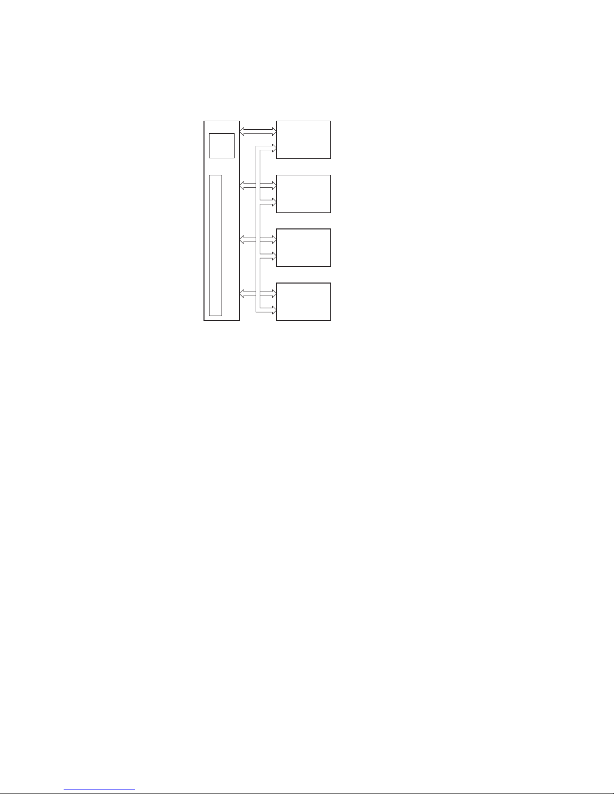
3.1.12 TSP
The TSP board is the central control unit in the ADE. Its main task is to control the antenna pointing
stabilisation, satellite search and satellite tracking. In addition it takes care of control data communication
with the BDE, synthesizer setup and locking surveillance, and exchange of control and status information
with the HPA controller. A block diagram is shown in fig. 3.13.
Memory block
V10
V9
V8
CPU
Connectors
D/A converter
Output section
Registers
+2.5V, -2.5V
+14V, +5V, -5V, -11V
Power supply
Measurement section
Buffer, filter
35967
Fig. 3.13.
The program code for the TSP is placed in two flash proms mounted in 32 pin plcc cases in one of the
corners of the board. The code is divided in an even and an odd part. The prom closest to the MC68HC16
CPU and the centre of the board holds the even code part, the other holds the odd part.
Exchanging proms
If replacement of the proms is needed, note that the software can be exchanged as physical PROM's or
as ADE upload (see section 6.1.2)
1) The main power must be off during the operation.
2) To distinguish between even/odd prom, see chapter 5.
3) Align the notched corner of the plcc’s with the cut corner of the sockets (alignment mark).
4) Before inserting the new proms in the socket be sure that no pins of the prom or the socket
have been bent or somehow misaligned in any way.
PAGE 3-14
9936
Page 35

3 MODULE DESCRIPTION Inmarsat B
The LEDs
The TSP board is equipped with 3 LEDs (smd types): A pair consisting of a red (V10) and a green (V9)
placed between the CPU and the SRAM and a red LED (V8) placed almost at the centre of the board.
V8, red LED, reset source indicator
This LED should normally always be on after power on/off reset and stay on as long as the
power is turned on. It must only be off after a soft reset (through service interface) or after a
software update by upload (also ending with a soft reset of the TSP). If this LED is turned off in
any other situation than described above a failure has occurred on the TSP board. Check to
see that the flash proms are correctly aligned and that no pins have been bent or damaged. If
this does not help, the proms or the complete TSP board must be replaced.
V9, green LED, test/debug LED
This LED is normally used for factory test and debug purposes.
During upload of a new program to the TSP, V9 will flash quickly each time a block of the new
program code has been received and stored in the TSP upload buffer.
If V9 does not flash during upload, no program data is received from the BDE, and it is most
likely that the upload does not work correctly. Check the interface between the service PC and
the BDE, and check if any error messages from the BDE are shown on the service interface
PC.
V10, red LED, alive indicator
This LED always flashes with a total period of 1 second. The flashing will pause a few seconds
after reset and then start flashing.
3.1.13 TILT SENSOR
The main component of this module is a dual axis tilt sensor, which is a vertical sensing electrolytic
potentiometer providing a linear voltage output as the unit is tilted around the horizontal axis. The unit is
a hermetically sealed glass enclosure with five internal electrodes. One common electrode is placed at
the vertical centre line, and two pairs of electrodes (called x and y direction) are placed on orthogonal
axes.
Because the sensor contains an electrolyte, the drive signal has to be an AC voltage. A block diagram
of the module is shown in fig. 3.14.
S & H
S & H
S & H
S & H
Network
Sampling
Network
Combiner
Network
Sampling
Sensor
multivibrator
Astable
X
Y
35969
Fig. 3.14.
The AC voltages for the four tilt sensor inputs are derived from an astable multivibrator and two frequency
divider circuits built up with D type flip flops. The AC voltages for the two x inputs are out of phase. This
is also the case with the y inputs.
The common output from the tilt sensor is connected to four sample and hold amplifiers. A combinatorial
network generates four sample and hold signals, one at a time, to the amplifiers. A subtraction circuit built
up with operational amplifiers combines the two x signals to a single signal which then is offset in
amplitude to generate zero output when the tilt angle is zero. The resulting y signal is made with a circuit
equal to the one used to generate the x signal.
PAGE 3-15
9849
Page 36

3 MODULE DESCRIPTION Inmarsat B
3.2 BELOW DECK EQUIPMENT
3.2.1 SPS BOARD
The SPS board consists of baseband for IF converters to both transmitter and receiver signal paths, data
receiver and transmitter equal to those placed on the triplexer board, the system reference oscillator and
a digital signal processor for carrier and clock synchronisation.
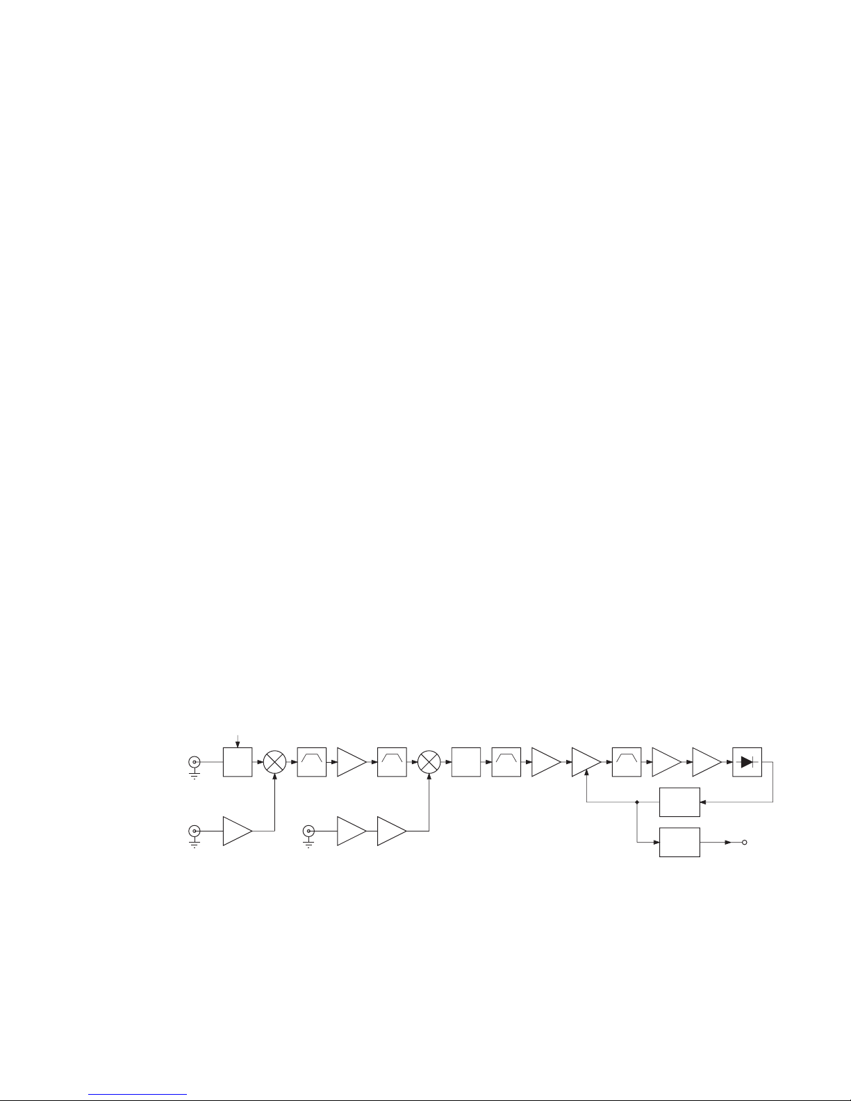
A block diagram of the SPS board is shown in fig. 3.2.1.
TX-Modulator
TX-LO
SC-LPF
SC-LPF
LO
TX-SC
Doubler
Freq.
OCXO
De-Modulator
DSP
RX-LO
LO
RX-SC
SC-LPF
SC-LPF
A/D
A/D
21.4 MHz
QuadPlexer
Shift Register
24 bit
99 MHz
TX
Data
RX
Data
87 MHz
87 MHz
OSC
Q-Data to modem
I-Data to modem
TX-I from modem
TX-Q from modem
40.32 MHz
20.16 MHz
12
12
4
4
35532
Fig. 3.2.1.
Transmitter path
The TX baseband signals (TX-I, TX-Q) generated at the modem board are filtered in a pair of switch
capacitor filters. The cut off frequency of those filters can be changed by changing the filter clock
frequency. The clock frequency is generated by the TX-SC synthesizer and depends on the selected
service type. The filtered signals are mixed with a 62.9 MHz local oscillator signal (TX-LO) in a quadrature
mixer to form the final TX IF signal. The 62.9 MHz transmitter local oscillator is built up around a traditional
PLL integrated circuit.
Receiver path
The 21.4 MHz IF signal from the antenna is taken out from the quadplexer and unwanted signals are
attenuated in the low-pass filter. The IF signal is down converted to baseband in a quadrature
demodulator. The demodulator as shown in fig 3.2.1 is built up around two passive double balanced diode
mixers. The RF input for the mixers is the 21.4 MHz IF signal split equally in amplitude and with the same
phase. The local oscillator signal for the two mixers is of equal amplitude and frequency but 90° out of
phase. This phase shift is made by shifting one of the oscillator signals +45° and the other -45°. The two
PAGE 3-16
9936
Page 37

3 MODULE DESCRIPTION Inmarsat B
I and Q baseband signals taken out of the IF ports of the mixers are amplified by operational amplifiers
before they are filtered in low-pass switch capacitor filters. Those filters are of the same type as those used
in the transmitter part. The cut off frequency of the filters is selected by the frequency of the RX-SC
synthesized oscillator. The output signals of the switch capacitor filters are further amplified before they
are sampled in two 12 bit analogue to digital converters. The data format out of these A/D converters is
a 12- bit parallel format converted to a serial bit stream in a 24 bit shift register. This serial bit stream
representing the sampled I and Q signals is clocked into the digital signal processor.
Data receiver
From the quadplexer, the data signal transmitted from the triplexer at the antenna unit is filtered out in
a 99 MHz bandpass filter. The data receiver is built up around the same FM integrated subsystem where
an 87 MHz crystal oscillator is used to down convert the 99 MHz data signal to a 12 MHz IF before the
data bit is recovered in the FM detector. The 4800 baud data stream is transferred to the CSP/VDP board.
Data transmitter
The data transmitter is built up as an FSK modulator equal to the one placed on the triplexer board. The
data stream which is received from the CSP/VDP board is modulated into a carrier of 87 MHz with a
frequency shift of ± 150 kHz. A high-pass filter with a cut off frequency of 83 MHz increases the isolation
between the 62.9 MHz transmitter signal and the vector modulator in the data transmitter to lower
intermodulation products. Finally the signal level from the data transmitter is amplified before it enters the
quadplexer.
Reference oscillator
Due to the rigorous frequency accuracy requirement over a relatively wide temperature range, an oven
controlled crystal oscillator of 20.16 MHz is used to derive all critical reference frequencies.
A frequency doubler generates a 40.32 MHz signal to the ADE.
PAGE 3-17
9936
Page 38

3 MODULE DESCRIPTION Inmarsat B
3.2.2 MODEM BOARD
The modem is the module which takes care of the coding/decoding of data/baseband signals.
Depending on which service types the transceiver unit covers, different modem configurations can be
found in it.
A combined modem (629347) covers all service types. It handles LSD as well as HSD, and TX as well
as RX.
The modem has two main functions:
- A modulator converts the digital transmission data to an analogue baseband signal (formed by an
I and a Q channel).
- A decoder converts the received digital baseband (also formed by an I and a Q channel, each
consisting of 4 parallel bits) to received data.
The modem employs Forward Error Correction (FEC) and scrambling (randomisation) techniques to
achieve the error free performance in accordance with Inmarsat requirements.
The block diagram shown in fig. 3.2.2 is for all modem variants.
detection &
Sync. word
ambiguity
resolution
decoder &
descrambler
Viterbi/
sequential Ser. interface
with VDP
Control
interface
with VDP
with VDP
Ser. interface
filters
shaping
Output
convolutional
coder
Scrambler
DAC
DAC
Rx
Status/control
Data
buffer
Bidir
Isymb.
Qsymb.
+3.3V
+5V
Power supply
Tx
Tx
Tx
35968
Fig. 3.2.2
A digital core performs all control, processing and communication as well as the outputting of data to the
A/D converters for the analogue output circuitry. The buffer, power and output circuitry is peripheral to
the digital core, which is formed by a single combi ASIC.
The following is a description of the interface to and from the PAX board:
X1: The modem is controlled through this connector via the TU bus (parallel interface) from the CSP/
VDP board. Certain data (telex and SUs) is provided to the modem through the TU bus. All
communication to and from the CSP runs in this connector.
X3: Serial synchronous interface to CSP/VDP board for TX and RX data. Also the reference clock and
some status signals pass through this connector.
X5 : Interfaces RX and TX baseband signals to the SPS board and provides power input (+7.5V and
-15V).
PAGE 3-18
9936
Page 39

3 MODULE DESCRIPTION Inmarsat B
3.2.3 CSP/VDP BOARD
The board (630953) is called the CSP/VDP module and consists basically of two functionally separate
parts. The CSP (control and signalling processor) is the main system processor, which takes care of the
satellite protocol, man/machine and external equipment interfaces. A block diagram of the module is
shown in fig. 3.2.3.
MUX
PCM
MUX
Clock
Gen.
VDP
ACIA
CSP
CAN
TU bus
Pax Board
From/to
Scanbus
Scanbus
ADE Data
NMEA
PC/Printer
Tubus
Alarm
35965A
Fig 3.2.3
The VDP (voice and data processor) is a digital signal processor which handles voice encoding and
decoding, and acts as the interface between the baseband modem and the PAX module for the fax and
data services.
The software for the CSP and VDP is contained in the same set of EPROMs and transferred by the CSP
to the VDP when powering on.
The CSP controls the signal routing around the VDP and has the following interface paths:
X1: Contains an 8-bit parallel data interface, is used to control all other boards in the
transceiver.
X2: Contains 5 asynchronous serial data interfaces for the telex terminal, telex printer, service
terminal, NMEA position and NMEA gyro. Inputs from the external distress buttons are
also connected through X2.
X3: Contains the asynchronous serial data interface to the antenna, which is modulated into a
carrier on the SPS board.
X4: Contains the scanbus which is the interface to the control units and future expansions. The CSP
is involved in the digital part through a data network called CAN (controller area network).
- The VDP is connected directly to the CSP data bus.
The VDP has the following interface paths:
X3: Contains a synchronous serial data interface to the baseband modem.
X4: Contains the audio part of the scanbus.
X7: Contains a synchronous data interface to the PAX module, used for the fax and data services.
PAGE 3-19
9936
Page 40

3 MODULE DESCRIPTION Inmarsat B
3.2.4 PAX BOARD
The PAX board (631593) is an advanced interface for data, facsimile and phones. The board is controlled
from the CSP/VDP board through the TU bus. The central processor on the pax board, AM186EM-40,
is an embedded version of the 186 processor, which is able to run on 186 code. The chosen processor
is faster than the 186, and has more built-in functions. A block diagram is shown in fig. 3.2.4.
MUX
SLIC
SLIC
Connector
Phone 1
Phone 2
ACIA
MUX
FAX
Control SCIA
To VDP
To VDP
PC/Printer
35966
Fig. 3.2.4.
The data part is fully hayes compatible, and capable of running high speed 64 kbps full duplex data as
well as 9600 kbps (ARQ/NARQ) full duplex data.
Connection to the PAX board is handled by a high speed ACIA, as in most modern PCs or modems.
The facsimile connection can be made through either of the two phone connectors, with a maximum
transmission speed of 9600 kbps. The handling of fax calls, the T.30 protocol used in all fax communication, and the DTMF tone detection are done by an integrated circuit.
Either of the two phone connectors can also be used for ordinary analogue telephones or PABX
connections. The system detects during startup if a PABX is connected, and automatically configures the
system for this. The phone system is fitted with an advanced voice guide which can guide the user through
the sequence of changing earth station and network. Two separate SLICs (subscriber line interface
circuits) handle the two phone connectors.
On the edge of the PAX board, 5 connectors are used to interface to the other boards in the transceiver
unit. A short description of each connector is given below:
X1: TU bus connection to the CSP/VDP board. All communication to and from the CSP
runs in this connector.
X2: Serial communication supply and +40V DC for the SLIC circuits.
X5: Analogue voice connection to CSP/VDP board, supply voltages and PABX interrupt.
X6: Connections to the two phone connectors, data and optional PC connections.
X7: Synchronous interface to and from the CSP/VDP board. Fax and data communication.
PAGE 3-20
9936
Page 41

3 MODULE DESCRIPTION Inmarsat B
3.2.5 SMI BOARD
The switch mode power supply and interconnection board consists basically of two independent units.
The interconnection takes care of the interface between SUB-D connectors at the rear panel of the
transceiver unit and the modules inside it. A block diagram is shown in fig. 3.2.5.
Power Ant. Scanbus NMEA Data Pc/Printer Alarm Phone 2 Phone 1
X1 X2 X3 X4
Ribbon cable connectors to transceiver modules
Rear panel connectors
Connection circuit
Filter 40V DC Conv. 40V DC Conv. 40V DC Conv. Multi Conv.
Control circuit DC/DC Conv.
-12V +12V +40V -15V +15V +24V +8V
35970
Fig. 3.2.5.
The supply voltage delivered from the ship to the transceiver unit is 24V DC nominal but can range from
20 to 40V DC. From the input voltage, the switch mode power supply generates the following voltages:
+40V DC - 7A
+12V DC - 0.1A
-12V DC - 0.1A
+15V DC - 0.25A
-15V DC - 0.15A
+7.5V DC - 2.6A
+24V DC - 0.4A
The switch mode power supply is built up as four converter modules, placed on a main board containing
all the DC control circuits. Three of the converter modules generate 40V DC and are coupled in parallel,
i.e. only one 40V DC is available. The fourth converter is a multi converter generating all internally used
voltages in the transceiver unit. The 40V DC is used as main voltage for the antenna unit, as input for the
multiconverter and finally as input for a special DC/DC converter placed on the main board generating
±12V DC for RS 232 terminals connected to the transceiver unit.
All the converters are placed inside a metal screen to prevent emission of noise. A heat sink is placed
on top of the converters. Therefore, when the transceiver unit is working, the blower inside the transceiver
unit must always be connected.
40V DC converter module
This module is a push-pull converter, basically controlled by a current mode controller, which is controlled
and synchronised by the control circuit on the main board.
Multiconverter module
This module contains two converters. The first one is a step DOWN converter converting the 40V DC
down to 7.5V DC which supplies the 5V regulators placed on the different boards inside the transceiver
unit.
The second converter is a fly back version, which creates ±15V DC for the transceiver modules and +24V
DC mainly used to supply the control unit and handset.
The multiconverter is also synchronised with the 40V DC converters.
PAGE 3-21
9936
Page 42

3 MODULE DESCRIPTION Inmarsat B
3.2.6 HANDSET
The handset is connected to the transceiver unit through the Scanbus which contains both analogue and
digital signals. The analogue signals are microphone signal from handset and loudspeaker signal to the
handset. Both signals are balanced.
PAGE 3-22
9936
Page 43

CONTENTS
4 ACCESSORIES 4-1
4.1 SC4350 CONTROL UNIT 4-1
4.2 SD4360 DISTRESS BUTTON 4-1
4.3 H4394/95 VERITAS CONNECTION BOX 4-1
4.4 H4396 T-CONNECTION BOX 4-2
9849
Inmarsat B
Page 44

4 ACCESSORIES
This chapter describes units which can be connected to the transceiver unit. These include both control
units and units used for installation.
4.1 SC4350 CONTROL UNIT
The Control Unit SC4350 is a desk/bulkhead mounted keyboard/display unit, using a handset without
display/keyboard. Normal user interface, as well as system setup, can be carried out from the unit. All
operations are performed from the unit’s front panel.
In all essentials, the functions of the Control Unit SC4350 are the same as those of the Handset SC4345.
The Control Unit SC4350 can be used instead of the Handset SC4345, or it can be used as an additional
Control Unit, as a total of up to 5 Handsets/Control Units can be connected to the system.
To BDE
Circuits
Analogue
Keyboard
Transceiver
Micro-
processor
Circuits
+24V
Speaker
Display
Handset
36823
The Control Unit SC4350 is connected to the BDE transceiver via the so-called “Scanbus”, which contains
digital communications (Canbus), audio-frequency signals (2 “twisted pairs”, balanced lines, one for each
direction, microphone to BDE transceiver, and BDE transceiver to earpiece/loudspeaker), and powersupply wires. Connection may be directly to the BDE transceiver’s “Scanbus” connector, or via a “Veritas
connection box”. If more than one Control Unit are to be connected to the system, H4396 connection
boxes are used. All connected Control Units are 100% electrically parallelled.
The unit is not “intelligent”. When for example a key is pressed, information about which key was pressed,
is passed to the BDE transceiver, which interprets the key-press code and returns new display
information, signal path setup information, sounder setup, or whatever may be relevant in the given
situation. The SC4350 then executes these commands.
Please note, in case of service or repair: The unit can do virtually nothing if not connected to a BDE
transceiver.
4.2 SD4360 DISTRESS BUTTON
The distress button can be used in connection with a push button telephone or a telex terminal. The
function is the same as the one placed in the handset hook. A block diagram is shown in fig. 4.3.
Key
Distress
Timer
To/from
Indicator
Converter
Level
Regulator
Voltage
Alarm Connector
35533
Fig. 4.3.
PAGE 4-1
9936
Inmarsat B
Page 45

4 ACCESSORIES Inmarsat B
PAGE 4-2
9936
Component location Veritas connection box
The distress key activates a timer circuit which generates a 9 Hz square wave voltage until the key is
released. The square wave voltage is modified in the level converter to interface to the open collector
circuit in the alarm connector.
An indicator circuit consisting of light and a 3 kHz tone is activated from the alarm connector during a
distress alert.
A voltage regulator generates the needed 12V DC to the timer and indicators.
4.3 H4394/95 VERITAS CONNECTION BOX
A Veritas connection box is the interface between the SUB-D connectors at the transceiver unit rear panel
and the ship installations. A diagram and component placements are shown below. All SUB-D connectors
at the transceiver unit are connected to their respective SUB-D connectors inside the Veritas connection
box. In the box, connections between SUB-D and the wire terminal blocks to the ships installation cables
are made.
Two relays inside the Veritas connection box can be used to activate externally mounted indicators on
the ship like alarms, horns, lamps etc. The relays, if used, can be connected to the alarm connector and
indicate service announcements or distress transmitted. The functions of the relays are set up during
installation.
A gyro repeater is also included and can be used if the NMEA signal from the ship gyro compass
is not available.
Page 46

4 ACCESSORIES Inmarsat B
PAGE 4-3
Inmarsat B
9849
Diagram Veritas connection box
Page 47

4 ACCESSORIES Inmarsat B
PAGE 4-4
9901
4.4 H4396 T-CONNECTION BOX
Component location T-Connection box
Diagram T-Connection box
Page 48

CONTENTS
5 DISASSEMBLING, CONNECTORS, MODULE AND
SOFTWARE LOCATION 5-1
5.1 ANTENNA UNIT 5-1
5.1.1 MODULE AND SENSOR LOCATION 5-1
5.1.2 MECHANICAL DISASSEMBLING 5-2
5.1.2.1 CHANGING AZIMUTH TIMING BELT 5-2
5.1.2.2 CHANGING ELEVATION TIMING BELT 5-2
5.1.2.3 CHANGING CROSS ELEVATION TIMING BELT 5-2
5.1.2.4 CHANGING HORIZONTAL AXIS TIMING BELT 5-3
5.1.3 CONNECTORS AND SOFTWARE LOCATION 5-4
5.1.3.1 UP/DOWN CONVERTER UNIT 5-4
5.1.3.2 TRACKING RECEIVER UNIT 5-5
5.1.3.3 HPA 5-6
5.1.3.4 DIPLEXER/LNA 5-7
5.1.3.5 TSP 5-7
5.1.3.6 TRIPLEXER 5-10
5.1.3.7 SMPS 5-11
5.1.3.8 STEP MOTOR DRIVER 5-13
5.1.3.10 DC MOTOR DRIVER 5-14
5.1.3.11 TILT SENSOR 5-15
5.1.3.12 FLUXGATE COMPASS 5-15
5.1.3.13 ZERO-MARK DETECTOR 5-16
5.1.3.14 INTERCONNECTION BOARD 5-16
5.2 TRANSCEIVER UNIT 5-17
5.2.1 MODULE LOCATION 5-17
9849
Inmarsat B
Page 49

CONTENTS Inmarsat B
9936
5.2.2 CONNECTORS AND SOFTWARE LOCATION 5-18
5.2.2.1 SPS BOARD 5-22
5.2.2.2 CSP/VDP BOARD 5-22
5.2.2.3 PAX BOARD 5-23
5.2.2.4 SMI 5-23
5.2.2.5 LSD, HSD FPGA AND COMBI MODEM 5-24
5.3 HANDSET 5-25
5.3.1 SOFTWARE LOCATION 5-25
5.4 CONTROL UNIT 5-25
5.4.1 SOFTWARE LOCATION 5-25
Page 50

PAGE 5-1
9936
5 DISASSEMBLING, CONNECTORS, MODULE AND SOFTWARE LOCATION
5.1 ANTENNA UNIT
5.1.1 MODULE AND SENSOR LOCATION
1
6
2
7
3
4
8
5
Fig. 5.1
1. Tracking receiver unit part no. 729840
2. HPA part no. 729430
3. Diplexer/LNA part no. 730630
4. DC motor controller for cross elevation axis part no. 634686
5. Step motor driver for horizontal axis part no. 629362
6. Step motor driver for elevation axis motor part no. 629362
7. SMPS part no. 629364
8. Rate sensor for cross elevation axis part no. 41.603
9. ADE fuse part no. 45.510
Fig. 5.2
1. Up/down converter unit part no. 730650
2. Connection board part no. 629349
3. Triplexer part no. 629358
4. TSP part no. 630814
5. Step motor driver for azimuth axis part no. 629362
Fig. 5.3
1. ADE on/off switch
2. Tilt sensor part no. 629366
3. Rate sensor for elevation axis part no. 41.603
4. Rate sensor for azimuth axis part no. 41.603
1
5
1
2
3
4
2
3
4
9
Inmarsat B
Page 51

5 MECHANICAL DISASSEMBLING AND MODULE LOCATION Scansat-B
PAGE 5-2
9936
1
2
5.1.2 MECHANICAL DISASSEMBLING
5.1.2.1 CHANGING AZIMUTH TIMING BELT
Fig. 5.4
1. Loosen the four screws holding the motor part no. 87.434
2. Remove the 3 mm screw holding
the connection print part no. 86.962
3. Remove three 2.5 mm screws, and
remove the connection print part no. 86.004
Change the timing belt.
3
5.1.2.2 CHANGING ELEVATION TIMING BELT
Fig. 5.5
1. Remove the plug from the motor driver pcb
2. Loosen the four screws holding the motor part no. 87.443
3. Remove one 4 mm screw part no. 87.285
4. Remove twelve 3 mm screws part no. 86.963
5. Remove six 4 mm screws part no. 87.285
6. Remove three 8 mm bolts part no. 87.902
7. Remove the side panel part no. 230623
Change the timing belt.
*
*
*
*
*
*
*
*
*
*
*
*
1
4
*
3
#
#
#
#
#
#
5
#
6
7
§
§
§
§
2
§
5.1.2.3 CHANGING CROSS ELEVATION TIMING BELT
Fig. 5.6
1. Loosen the four screws holding the motor
Lower screws part no. 87.452
Upper screws part no. 87.453
2. Remove two 5 mm screws part no. 87.453
and the timing belt lock part no. 63.612
Change the timing belt.
2
1
part no. 48.853
part no. 736888
part no. 736889
part no. 736889
part no. 48.852
part no. 530663
part no. 736890
Page 52

5 MECHANICAL DISASSEMBLING AND MODULE LOCATION Inmarsat B
PAGE 5-3
9936
5.1.2.4 CHANGING HORIZONTAL AXIS TIMING BELT
Fig. 5.7
1. Loosen the four screws holding the motor part no. 86.962
2. Loosen one 5 mm bolt, part no. 87.421
and remove the horizontal axis
Change the timing belt.
2
1
part no. 48.855
part no. 736891
Page 53

5 MECHANICAL DISASSEMBLING AND MODULE LOCATION Inmarsat B
PAGE 5-4
9905
5.1.3 CONNECTORS AND SOFTWARE LOCATION
5.1.3.1 UP/DOWN CONVERTER UNIT
PART no.: 730650
Connections:
Connector no.: X1, X2, X3, X4, X5
Connector type: SMA, Coax
Connector no. Connection name To/from
X1 62.9 MHz input to up converter Triplexer
X2 L-band output from up converter HPA
X3 10.08 MHz reference to synthesiser Triplexer
X4 21.4 MHz IF from down converter Triplexer
X5 L-band input to down conv erter Diplexer/LNA unit
Connector no.: X6
Connector type: Molex, 2 x 10 pins
Pin no. Connection name Colour To/from
1 No connection
2 No connection
3 -15.5V DC Brown SMPS
4 Ground Black
5 +18V DC Orange SMPS
6 +8V DC Red SMPS
7 STB2 LO2 D White TSP
8STB LO1 D Violet TSP
9 LOCK DET 1 Violet TSP
10 STB1 LO2 D Grey TSP
11 STB LO2 U Green TSP
12 LOCK DET 2 Blue TSP
13 STB1 LO1 U Green TSP
14 STB2 LO1 U Blue TSP
15 STBD Grey TSP
16 RXL White TSP
17 GROUND Black
18 STBU Violet TSP
19 DATA Green TSP
20 CLOCK Blue TSP
X3
X6
X4
X5
X1
X2
Page 54

5 MECHANICAL DISASSEMBLING AND MODULE LOCATION Inmarsat B
9905
PAGE 5-5
5.1.3.2 TRACKING RECEIVER UNIT
PART no.: 729840
Connections:
Connector no.: X1, X3
Connector type: SMA, Coax
Connector no. Connection name To/from
X1 L-band input to tracking receiver Diplexer/LNA unit
X3 10.08 MHz reference to synthesiser Triplexer
Connector no.: X2
Connector type: Molex, 14 pins
Pin no. Connection name Colour To/from
1 No connection
2 No connection
3 -15.5V DC Brown SMPS
4 Ground Black
5 +18V DC Orange SMPS
6 +8V DC Red SMPS
7 Ground Black
8 STS Green TSP
9 STB2 LO2 T White TSP
10 STB LO1 T Blue TSP
11 CLOCK Violet TSP
12 STB1 LO2 T Grey TSP
13 LOCK DET Green TSP
14 DATA Blue TSP
X3
X2
X1
Page 55

5 MECHANICAL DISASSEMBLING AND MODULE LOCATION Inmarsat B
5.1.3.3 HPA
PART no.: 729430
Connections:
Connector no.: X1, X2
Connector type: SMA, Coax
Connector no. Connection name To/from
X1 Output from HPA Diplexer
X2 Input to HPA Up converter
Connector no.: X3
Connector type: Molex, 2 X 10 pins
Pin no. Connection name Colour To/from
1 +28RV DC Yellow SMPS
2 +28RV DC Yellow SMPS
3 +28RVDC Yellow SMPS
4 Ground Black SMPS
5 +28V Orange SMPS
6 Ground Black SMPS
7 +12V Orange SMPS
8 Ground Black SMPS
9 +7.5V Red SMPS
10 Test TSP
11 DMB 2 Blue SMPS
12 STB PC Green TSP
13 CLK White TSP
14 DATA Grey TSP
15 Ground Black SMPS
16 DATA OUT White TSP
17 DATA IN Grey TSP
18 CLK Violet TSP
19 SS Blue TSP
20 PORT Green TSP
PAGE 5-6
9905
X1
X2
X3
Page 56

5 MECHANICAL DISASSEMBLING AND MODULE LOCATION Inmarsat B
5.1.3.4 DIPLEXER/LNA
PART no.: 730630
Connections:
Connector no.: X1, X2, X3, X4
Connector type: SMA, Coax
Connector no. Connection name To/from
X1 LNA out put Down converter
X2 LNA out put Tracking rec eiver
X3 Diplexer input/output Antenna
X4 Diplexer input, Tx HPA
5.1.3.5 TSP
PART no.: 630814
PAGE 5-7
9849
X3
X4
X1
X2
Page 57

5 MECHANICAL DISASSEMBLING AND MODULE LOCATION Inmarsat B
Software:
Component no. Description Spare part no.
D15 Tracking & stabilisation 732514
D16 Tracking & stabilisation 732515
Connections:
Connector no.: X19
Connector type: 3M, 2 x 5 pins
Pin no. Connection name Colour To/from
1 +18V Grey, ribbon cable SMPS
2 +8V Grey, ribbon cable SMPS
3 +8V Grey, ribbon cable SMPS
4 -15.5V Grey, ribbon cable SMPS
5 Ground Grey, ribbon cable SMPS
6 DMB_1 Grey, ribbon cable SMPS
7 RXD_FROM_BDE Grey, ribbon cable Triplexer
8 TXD_TO_BDE Grey, ribbon cable Triplexer
9 No connection Grey, ribbon cable
10 No connection Grey, ribbon cable
Connector no.: X20
Connector type: MOLEX, 2 x 12 pins
Pin no. Connection name Colour To/from
1 LOCKDET_T Green Tracking receiver unit
2 SYNTH_DATA Blue Tracking receiv er unit
3 SYNTH_SCLK Violet Tracking receiver unit
4 STB1LO2T Grey Tracking receiv er unit
5 STB2LO2T White Tracking receiver unit
6 STBLO1T Blue Tracking receiver unit
7 Ground Black Tracking receiver unit
8 Tracklevel Green Tracking receiver unit
9 SYNTH_DATA Green Up/Down converter unit
10 SYNTH_SCLK Blue Up/Down converter unit
11 Ground Black Up/Down converter unit
12 STBU v iolet Up/Down converter unit
13 STBD Grey Up/Down converter unit
14 No connection White Up/Down converter unit
15 STB1LO1U Green Up/Down converter unit
16 STB2LO1U Blue Up/Down converter unit
17 STBLO2U Green Up/Down converter unit
18 LOCK_DET1 Blue Up/Down converter unit
19 LOCKDET_2 Violet Up/Down converter unit
20 STB1LO2D Grey Up/Down converter unit
21 STB2LO2D White Up/Down converter unit
22 STBLO1D Violet Up/Down converter unit
23 No connection
24 No connection
PAGE 5-8
9905
Page 58

5 MECHANICAL DISASSEMBLING AND MODULE LOCATION Inmarsat B
Connector no.: X22
Connector type: MOLEX, 2 x 3 pins
Pin no. Connection name Colour To/from
1 HPA_SEL Green HPA
2 HPA_READ_REQ Blue HPA
3 HPA_DATA_CLOCK Violet HPA
4 HPA_DATA_TO_HPA Grey HPA
5 HPA_DATA_FROM_HPA White HPA
6 Ground Black HPA
Connector no.: X24
Connector type: MOLEX, 2 x 20 pins
Pin no. Connection name Colour To/from
1 El_PHASE_A Green Step motor driver, El
2 Ground Black Step motor driver, El
3 El_PHASE_B Blue Step motor driver, El
4 El_PHASE_C Violet Step motor driver, El
5 No connection
6 El_PHASE_D Grey Step motor driver, El
7 CE_PHASE_A Green Motor driver, CE
8 Ground Blac k Motor driver, CE
9 CE_PHASE_B Blue Motor driver, CE
10 CE_PHASE_C Violet Motor driver, CE
11 No connection
12 CE_PHASE_D Grey Motor driver, CE
13 No connection
14 No connection
15 CE_RATE White Rate sensor, CE
16 No connection
17 X4_PHASE_A Green Step motor driver, HZ
18 Ground Black Step motor driver, HZ
19 X4_PHASE_B Blue Step motor driver, HZ
20 X4_PHASE_C Violet Step motor driver, HZ
21 No connection
22 X4_PHASE_D Grey Step motor driver, HZ
23 X4_ZERO White Zero mark det.
24 Ground Black Zero mark det.
25 FLXG_Y Violet Fluxgate compass
26 FLXG_X Grey Fluxgate compass
27 Ground Black Fluxgate compass
28 No connection
29 Tilt_X Blue Tilt sensor
30 Tilt_Y Violet Tilt sensor
31 Ground Black Tilt sensor
32 No connection
33 No connection
34 Az_RATE_OFFSET White Motor driver, CE
35 Az_Rate White Rate sensor, Az
36 No connection
37 No connection
38 No connection
39 El_Rate White Rate sensor, El
40 No connection
PAGE 5-9
9849
Page 59

5 MECHANICAL DISASSEMBLING AND MODULE LOCATION Inmarsat B
Connector no.: X27
Connector type: MOLEX, 2 x 5 pins
Pin no. Connection name Colour To/from
1 AZ_PHASE_A Green Step motor driver, Az
2 Ground Black Step motor driver, Az
3 AZ_PHASE_B Blue Step motor driver, Az
4 AZ_PHASE_C Violet Step motor driver, Az
5 No connection
6 AZ_PHASE_D Grey Step motor driver, Az
7 AZENC_PHA Green Not used
8 AZENC_PHB Blue Not used
9 Ground Black Not used
10 No connection
5.1.3.6 TRIPLEXER
PART no.: 629358
Connections:
Connector no.: X2, X3, X4, X5, X6
Connector type: SMB, coax
Connector no. Connection name To/from
X2 Composite input/output signal Connection board
X3 21.4 MHz IF signal Down converter
X4 62.9 MHz IF signal Up converter
X5 10.08 MHz reference signal Up/down converter
X6 10.08 MHz reference signal Tracking receiver
PAGE 5-10
9905
Page 60

5 MECHANICAL DISASSEMBLING AND MODULE LOCATION Inmarsat B
Connector no.: X1
Connector type: 3M, 2 x5 pins
Pin no. Connection name Colour To/from
1 +18V DC Grey ribbon cable SMPS/Tsp
2 +8V DC Grey ribbon cable SMPS/Tsp
3 +8V DC Grey ribbon cable SMPS/Tsp
4 No connection Grey ribbon cable SMPS/Ts p
5 Ground Grey ribbon cable SMPS/Tsp
6 No connection Grey ribbon cable SMPS/Ts p
7 Rx data Grey ribbon cable SMPS/Tsp
8 Tx data Grey ribbon cable SMPS/Tsp
9 No connection Grey ribbon cable SMPS/Ts p
10 No connection Grey ribbon cable SMPS/Tsp
5.1.3.7 SMPS
PART no.: 629364
P5P3
P6
P4
P2
P1
29364A50
F1
Fuse:
Component no. Description Spare part no.
F1 Fuse for 40V conv. 45.510
Connector no.: P1
Connector type: 2 x 2 pins
Pin no. Connection name Colour To/from
1 +40V Red Inter connection board
2 Ground Black Inter connection board
3 +40V Red Inter connection board
4 Ground Black Inter connection board
PAGE 5-11
9936
Page 61

5 MECHANICAL DISASSEMBLING AND MODULE LOCATION Inmarsat B
Connector no.: P2
Connector type: 2 x 7 pins
Pin no. Connection name Colour To/from
1 +28RV Yellow HPA
2 +28RV Yellow HPA
3 +28RV Yellow HPA
4 Ground Black HPA
5 +28V Orange HPA
6 Ground Black HPA
7 +12V Orange HPA
8 Ground Black HPA
9 +7.5V Red HPA
10 No connection
11 DMB2 Blue HPA
12 STB PC Green HPA
13 CLK White HPA
14 DATA Grey HPA
Connector no.: P3
Connector type: 2 x 8 pins
Pin no. Connection name Colour To/from
1 +24V Yellow Step motor driver, El
2 Ground Black Step motor driver, El
3 +24V Yellow BLDC motor driv er, Ce
4 Ground Black B LDC motor driver, Ce
5 +24V Yellow Step motor driver, Horison.
6 Ground Black Step motor driver, Horison.
7 +18V Not used
8 -15.5V Not used
9 Ground Black Rate sensor, CE
10 +8V Red Zero mark det.
11 Ground Black Zero mark det.
12 +18V Orange Compass
13 +8V Red Compass
14 -15.5V Brown Compass
15 Ground Black Compass
16 No connection
Connector no.: P4
Connector type: 2 pins
Pin no. Connection name Colour To/from
1 +28V Red Fan
2 Ground Blue Fan
PAGE 5-12
9905
Page 62

5 MECHANICAL DISASSEMBLING AND MODULE LOCATION Inmarsat B
Connector no.: P5
Connector type: 2 x 6 pins
Pin no. Connection name Colour To/from
1 +24V Yellow AZ motor driver
2 Ground Blac k AZ mot or driver
3 +5V Red Not used
4 Ground Black Not used
5 +18V Orange Up/Down converter unit
6 +8V Red Up/Down converter unit
7 -15.5V Brown Up/Down converter unit
8 Ground Black Up/Down converter unit
9 +18V DC Orange Track ing receiver unit
10 +8V DC Red Tracking receiver unit
11 -15.5V DC Brown Tracking receiver unit
12 Ground Black Tracking receiver unit
Connector no.: P6
Connector type: 2 x 5 pins
Pin no. Connection name Colour To/from
1 +18V DC Grey ribbon cable Triplexer/Tsp
2 +8V DC Grey ribbon cable Triplexer/Tsp
3 +8V DC Grey ribbon cable Triplexer/Tsp
4 No connection Grey ribbon cable Triplexer/Tsp
5 Ground Grey ribbon cable Triplexer/Tsp
6 No connection Grey ribbon cable Triplexer/Tsp
7 Rx data Grey ribbon cable Triplexer/Tsp
8 Tx data Grey ribbon cable Triplexer/Tsp
9 No connection Grey ribbon cable Triplexer/Tsp
10 No connection Grey ribbon cable Triplexer/Tsp
5.1.3.8 STEP MOTOR DRIVER
PART no.: 629362
P2
29362-50
P1
Connector no.: P1
Connector type: 2 x 4 pins
Pin no. Connection name Colour To/from
1 Phase A Green TSP
2 Ground Black TSP
3 Phase B Blue TSP
4 Phase C Violet TSP
5 No connection
6 Phase D Grey TSP
7 +24V DC Yellow SMPS
8 Ground Black SMPS
PAGE 5-13
9905
Page 63

5 MECHANICAL DISASSEMBLING AND MODULE LOCATION Inmarsat B
Connector no.: P2
Connector type: 2 x 3 pins
Pin no. Connection name Colour To/from
1 Phase A Blue Step motor
2 No connection
3 Phase B Red Step motor
4 Phase C Green Step motor
5 No connection
6 Phase D Black Step motor
5.1.3.10 DC MOTOR DRIVER
PART no.: 634686
Connector no.: X1
Connector type: 2 x 5 pins
Pin no. Connection name Colour To/from
1 WC Orange Motor
2 Ground Black Motor
3WB Red Motor
4 H3 White Motor
5WA Brown Motor
6 H2 Blue Motor
7 No connection
8 H1 Grey Motor
9 +5V Violet Motor
10 Ground Black Motor
Connector no.: X2
Connector type: 2 x 4 pins
Pin no. Connection name Colour To/from
1 No connection
2 Ground Green TSP
3 No connection
4 Break Violet TSP
5Ref White TSP
6 Phase Grey TSP
7 +24V DC Yellow SMPS
8 Ground Black SMPS
PAGE 5-14
9905
Page 64

5 MECHANICAL DISASSEMBLING AND MODULE LOCATION Inmarsat B
5.1.3.11 TILT SENSOR
PART no.: 629366
P1
29366-50
Connector no.: P1
Connector type: 2 x 4 pins
Pin no. Connection name Colour To/from
1 No connection
2 X output Blue TSP
3 Y output Violet TSP
4 Ground Black TSP
5 +18V DC Orange Fluxgate compass
6 +8v DC Red Flux gate compas s
7 -15.5V DC Brown Fluxgate compas s
8 Ground Black Fluxgate compass
5.1.3.12 FLUXGATE COMPASS
PART no.: 629369
P2
P3
29369-50
Connector no.: P2
Connector type: 2 x 6 pins
Pin no. Connection name Colour To/from
1 +18V DC Orange Tilt sensor
2 +8V DC Red Tilt sensor
3 -15.5V DC Brown Tilt sensor
4 Ground Black Tilt sensor
5 Not used
6 +12V DC Yellow Rate sensor EL
7 Not used
8 Ground Black Rate sensor EL
9 Not used
10 +12V DC Yellow Rate sensor CE
11 Not used
12 Not used
PAGE 5-15
9905
Page 65

5 MECHANICAL DISASSEMBLING AND MODULE LOCATION Inmarsat B
Connector no.: P3
Connector type: 2 x 5 pins
Pin no. Connection name Colour To/from
1 +12V DC Test point
2 +5V DC Test point
3 +18V DC Orange SMPS
4 +8V DC Red SMPS
5 -15.5V DC Brown SMPS
6 Ground Ground SMPS
7 Compass x output Violet TSP
8 Compass y output Grey TSP
9 -12V DC Test point
10 Ground Black TSP
5.1.3.13 ZERO-MARK DETECTOR
PART no.: 629365
P1
29365-50
Connector no.: P1
Connector type: Molex, 2 x 3 pins
Pin no. Connection name Colour To/from
1 Zero mark White TSP
2 Ground Black TSP
3 +8V DC Red SMPS
4 Ground Black SMPS
5 No connection
6 No connection
5.1.3.14 INTERCONNECTION BOARD
PART no.: 629349
Connector no.: X3
Connector type: Molex, 2 x 2 pins
Pin no. Connection name Colour To/from
1 +40V DC Red SMP S
2 Ground Black SMPS
3 +40V DC Red SMP S
4 Ground Black SMPS
PAGE 5-16
9905
Page 66

5 MECHANICAL DISASSEMBLING AND MODULE LOCATION Inmarsat B
5.2 TRANSCEIVER UNIT
5.2.1 MODULE LOCATION
CSP/VDP MODULE
LSD/HSD COMBI MODEM
629347
630953
PAX MODULE
631593
SPS MODULE
631531
SMI MODULE
631800
32332C
PAGE 5-17
9936
Page 67

5 MECHANICAL DISASSEMBLING AND MODULE LOCATION Inmarsat B
5.2.2 CONNECTORS AND SOFTWARE LOCATION
Connectors:
Connector no.: X1
Connector type: Micro match, 20 pins
Pin no. Connection name To/from
1 Ground ALL boards
2 ADDR0 ALL boards
3 ADDR1 ALL boards
4 ADDR2 ALL boards
5 ADDR3 ALL boards
6 DATA0 ALL boards
7 DATA1 ALL boards
8 DATA2 ALL boards
9 DATA3 ALL boards
10 DATA4 ALL boards
11 DATA5 ALL boards
12 DATA6 ALL boards
13 DATA7 ALL boards
14 STROBE0 ALL boards
15 STROBE1 ALL boards
16 STROBE2 ALL boards
17 STROBE3 ALL boards
18 No connection ALL boards
19 Reset ALL boards
20 Ground ALL boards
Connector no.: X2
Connector type: Micro match, 20 pins
Pin no. Connection name To/from
1 RS232 TLX RX SMI,PAX,CSP
2 RS232 TLX TX SMI,PAX,CSP
3 RS232 PRN TX SMI,PAX,CSP
4 RS232 GROUND SMI,PAX,CSP
5 RS232 PRN RX SMI,PAX,CSP
6 RS232 +12V SMI,PAX,CSP
7 RS232 -12V SMI,PAX,CSP
8 RS232 PRN CTS SMI,PAX,CSP
9 RS232 MON RX SMI,PAX,CSP
10 RS232 MON TX SMI,PAX,CSP
11 POSITION RX+ SMI,PAX,CSP
12 POSITION RX- SMI,PAX,CSP
13 GYRO RX+ SMI,PAX,CSP
14 GYRO RX- SMI,PAX,CSP
15 GROUND SMI,PAX,CSP
16 +40V SMI,PAX,CSP
17 BUTTON1 SMI,PAX,CSP
18 BUTTON2 SMI,PAX,CSP
19 FACTORY RESET SMI,PAX,CSP
20 GROUND SMI,PAX,CSP
PAGE 5-18
9849
Page 68

5 MECHANICAL DISASSEMBLING AND MODULE LOCATION Inmarsat B
Connector no.: X3
Connector type: Micro match, 20 pins
Pin no. Connection name To/from
1 Ground SPS,HSD,LSD,VDP/CSP
2 RCLK SPS,HSD,LSD,VDP/CSP
3 RFS SPS,HSD,LSD,VDP/CSP
4 RDATA SPS,HSD,LSD,VDP/CSP
5 TCLK SPS,HSD,LSD,VDP/CSP
6 TFS SPS,HSD,LSD,VDP/CSP
7 TDATA SPS,HSD,LSD,VDP/CSP
8 RX SIGNAL SPS,HSD,LSD,VDP/CSP
9 TX KEY SPS,HSD,LSD,VDP/CSP
10 MODEM CHANGE SPS,HSD,LSD,VDP/CSP
11 Ground SPS,HSD,LSD,VDP/CSP
12 CLOCK SPS,HSD,LSD,VDP/CSP
13 Ground SPS,HSD,LSD,VDP/CSP
14 NO CONNECTION SPS,HSD,LSD,VDP/CSP
15 NO CONNECTION SPS,HSD,LSD,VDP/CSP
16 ANT RX DATA SPS,HSD,LSD,VDP/CSP
17 ANT TX DATA SPS,HSD,LSD,VDP/CSP
18 NO CONNECTION SPS,HSD,LSD,VDP/CSP
19 NO CONNECTION SPS,HSD,LSD,VDP/CSP
20 Ground SPS,HSD,LSD,VDP/CSP
Connector no.: X3A
Connector type: Micro match, 20 pins
Pin no. Connection name To/from
1 Ground SPS,SMI
2 DATA RX SPS,SMI
3 DATA TX SPS,SMI
4 DATA RTS SPS,SMI
5 DATA CTS SPS,SMI
6 DATA DTR SPS,SMI
7 DATA DSR SPS,SMI
8 PC RX SPS,SMI
9 PC TX SPS,SMI
10 -15V SPS,SMI
11 +15V SPS,SMI
12 +7.5V SPS,SMI
13 -7.5V SPS,SMI
14 Ground SPS,SMI
15 PHONE1+ SPS,SMI
16 PHONE1- SPS,SMI
17 Ground SPS,SMI
18 PHONE2+ SPS,SMI
19 PHONE2- SPS,SMI
20 Ground SPS,SMI
PAGE 5-19
9849
Page 69

5 MECHANICAL DISASSEMBLING AND MODULE LOCATION Inmarsat B
Connector no.: X4
Connector type: Micro match, 8 pins
Pin no. Connection name To/from
1 Ground SMI,CSP
2 DATA+ SMI,CSP
3 DATA- SMI,CSP
4 RXAF+ SMI,CSP
5 AF+ SMI,CSP
6 RXAF- SMI,CSP
7 AF- SMI,CSP
8 Ground SMI,CSP
Connector no.: X5
Connector type: Micro match, 20 pins
Pin no. Connection name To/from
1 Ground SPS,PAX,HSD,LSD,CSP
2 I-SIGNAL-BIT0 SPS,PAX,HSD,LSD,CSP
3 I-SIGNAL-BIT1 SPS,PAX,HSD,LSD,CSP
4 I-SIGNAL-BIT2 SPS,PAX,HSD,LSD,CSP
5 I-SIGNAL-BIT3 SPS,PAX,HSD,LSD,CSP
6 ANAINP SPS,PAX,HSD,LSD,CSP
7 -15V SPS,PAX,HSD,LSD,CSP
8 ANAOUT SPS,PAX,HSD,LSD,CSP
9 +15V SPS,PAX,HSD,LSD,CSP
10 +7.5V SPS,PAX,HSD,LSD,CSP
11 +7.5V SPS,PAX,HSD,LSD,CSP
12 Q-SIGNAL-BIT0 SPS,PAX,HSD,LSD,CSP
13 Q-SIGNAL-BIT1 SPS,PAX,HSD,LSD,CSP
14 Q-SIGNAL-BIT2 SPS,PAX,HSD,LSD,CSP
15 Q-SIGNAL-BIT3 SPS,PAX,HSD,LSD,CSP
16 SYMBOL SYNC SPS,PAX,HSD,LSD,CSP
17 TX I-SIGNAL SPS,PAX,HSD,LSD,CSP
18 TX Q-SIGNAL SPS,PAX,HSD,LSD,CSP
19 PABX IRQ SPS,PAX,HSD,LSD,CSP
20 Ground SPS,PAX,HSD,LSD,CSP
Connector no.: X6
Connector type: Micro match, 16 pins
Pin no. Connection name To/from
1 Ground SPS,PAX
2 DATA RX SPS,PAX
3 DATA TX SPS,PAX
4 DATA RTS SPS,PAX
5 DATA CTS SPS,PAX
6 DATA DTR SPS,PAX
7 DATA DSR SPS,PAX
8 PC RX SPS,PAX
9 PC TX SPS,PAX
10 Ground SPS,PAX
11 PHONE1+ SPS,PAX
12 PHONE1- SPS,PAX
13 Ground SPS,PAX
14 PHONE2+ SPS,PAX
15 PHONE2- SPS,PAX
16 Ground SPS,PAX
PAGE 5-20
9849
Page 70

5 MECHANICAL DISASSEMBLING AND MODULE LOCATION Inmarsat B
Connector no.: X7
Connector type: Micro match, 8 pins
Pin no. Connection name To/from
1 Ground CSP,PAX
2 PAX TX CLK CSP,PAX
3 PAX TX SYNC CSP,PAX
4 PAX TX DATA CSP,PAX
5 PAX RX CLK CSP,PAX
6 PAX RX SYNC CSP,PAX
7 PAX RX DATA CSP,PAX
8 Ground CSP,PAX
Connector no.: X8
Connector type: 2 pins
Pin no. Connection name Colour To/from
1 VB Red Battery pack, CSP
2 Ground Black Battery pack, CSP
Connector no.: X36
Connector type: Micro match, 16 pins
Pin no. Connection name To/from
1 Ground CSP, FRONT CONNECTOR
2 +40V CSP, FRONT CONNECTOR
3 RS232 Ground CSP , FRONT CONNECTOR
4 RS232 TLX RX CSP, FRONT CONNECTOR
5 RS232 TLX TX CSP, FRONT CONNECTOR
6 RS232 PRN RX CSP, FRONT CONNECTOR
7 RS232 PRN TX CSP, FRONT CONNECTOR
8 RS232 PRN CTS CSP, FRONT CONNECTOR
9 RS232 MON RX CSP, FRONT CONNECTOR
10 RS 232 MON TX CSP, FRONT CONNECTOR
11 POSITION RX+ CSP, FRONT CONNECTOR
12 POSITION RX- CSP, FRONT CONNECTOR
13 GYRO RX+ CSP , FRONT CONNECTOR
14 GYRO RX- CSP, FRONT CONNECTOR
15 TX INHIBIT CSP, FRONT CONNECTOR
16 No connection CSP, FRONT CONNECTOR
PAGE 5-21
9849
Page 71

5 MECHANICAL DISASSEMBLING AND MODULE LOCATION Inmarsat B
5.2.2.1 SPS BOARD
PART no.: 631531
X1 X3
X3A
X5 X6
D4
31531-56
Software:
Component no. Description Spare part no.
D4 Receive Synchronization 731520
Connectors: X1, X3, X3A, X5, X6
5.2.2.2 CSP/VDP BOARD
PART no.: 630953
X2X1 X3 X4 X5 X6 X7
30953-56
D16
D15
X8
Software:
Component no. Description Spare part no.
D15 CSP/VDP Software 732512
D16 CSP/VDP Software 732513
Connectors: X1, X2, X3, X4, X5, X6, X7, X8
PAGE 5-22
9936
Page 72

5 MECHANICAL DISASSEMBLING AND MODULE LOCATION Inmarsat B
5.2.2.3 PAX BOARD
PART no.: 631593
X1 X2
D19
D20
X5 X6
X7
31593-56
Software:
Component no. Description Spare part no.
D19 Phone & Fax Software 731523
D20 Phone & Fax Software 731522
Connectors: X1, X2, X5, X6, X7
5.2.2.4 SMI
PART no.: 731649
36832
F3
F2
F1
F4
F5
Fuses:
Component no. Description Spare part no.
F1 Main fuse - 20A 45.665
F2 Fuse for 40V conv. 45.510
F3 Fuse for 40V conv. 45.510
F4 Fuse for 40V conv. 45.510
F5 Fuse for NMEA - 40V 45.722
PAGE 5-23
9936
Page 73

5 MECHANICAL DISASSEMBLING AND MODULE LOCATION Inmarsat B
31800D
F2
F3
F4
F1
F5
X3 X2 X1X4
Connectors: X1, X2, X3, X4
5.2.2.5 LSD, HSD FPGA AND COMBI MODEM
PART no.: 629347
29346-56
X1 X3 X5
Connectors: X1, X3, X5
HS FPGA MODEM
PART no.: 633846
33847-56
PAGE 5-24
9936
Page 74

5 MECHANICAL DISASSEMBLING AND MODULE LOCATION Inmarsat B
PAGE 5-25
9936
COMBI MODEM
PART no.: 629347
29347-56
5.3 HANDSET
5.3.1 SOFTWARE LOCATION
PART no.: 630499
30499-56
D4
Component no. Description Spare part no.
D4 CU Software 735158
5.4 CONTROL UNIT
5.4.1 SOFTWARE LOCATION
PART no.: 633769
33769-56
D5
Component no. Description Spare part no.
D5 CU Software 735585
Page 75

CONTENTS
6 SERVICE INTERFACE 6-1
6.1 ADE 6-2
6.2 ALARM 6-4
6.3 BOOK 6-4
6.4 BUTTONS 6-5
6.5 CAN 6-5
6.6 CASC 6-5
6.7 COURSE 6-7
6.8 CU 6-7
6.9 DATE 6-9
6.10 EXIT 6-10
6.11 GYRO 6-10
6.12 HELP 6-10
6.13 LES 6-11
6.14 LOG 6-11
6.15 MODEM 6-12
6.16 NUMERIC 6-13
6.17 PAX 6-13
6.18 POSITION 6-14
6.19 PRINTER 6-14
6.20 REGION 6-15
6.21 REMARK 6-16
6.22 SES 6-16
6.23 SNU 6-17
6.24 SPEED 6-18
Inmarsat B
9936
Page 76

CONTENTS Inmarsat B
6.25 SPS 6-18
6.26 STATUS 6-19
6.27 SU 6-20
6.28 TEST 6-20
6.29 TIME 6-22
6.30 VDP 6-23
6.31 VERSION 6-23
9936
Page 77

PAGE 6-1
Inmarsat B
9905
6 SERVICE INTERFACE
The service interface is a useful software tool for both installation and servicing. It provides the technician
with detailed information about the system.
The service interface is intended for use with a personal computer running a terminal emulation program
like PROCOMM. The connections between the service PC and the transceiver unit and the settings of
the terminal program are all described below:
Connections
The electrical interface is compatible with RS232C. In order to protect it against
ground loops, it is isolated by opto-couplers, which makes it ideal for incidental
connections.
Only 3 wires need to be connected between the terminal and the transceiver unit,
labelled as follows:
Service RX: Data from PC to transceiver unit
Service TX: Data from transceiver unit to PC
Serial GND: Common
These signals are found in connector X34 (PC/printer port at the rear panel of the
transceiver unit).
The following table shows the connections to be made to a PC COM port with either
a 9- or 25-pin D-SUB connector.
Signal X34 PC, 9-pin SUB-D PC, 25-pin SUB-D
Service RX 13 3 2
Service TX 14 2 3
Serial GND 15 5 7
Settings
Although the terms may differ for different terminals, the PC or terminal emulation
program must be set up using the following parameters:
Baud rate: 9600 bps
Parity: Odd
Data bits: 7
Stop bits: 1
Mode: Full duplex
Local echo: Off
Hand shake: XON/XOFF (software)
DTR/DSR: Off
RTS/CTS: Off
Translation: OFF
Emulation: ASCII, TTY, VT52, VT100 or VT220
Before the actual description, each command has a syntax description. This is a single line for each
variant of the command. Optional parts are shown in square brackets like this:
POS[ITION]
which means that the position command may be typed as either POS or POSITION. When a choice of
completely different words are available, the vertical bar | is used like this:
NORTH|SOUTH
which means that the parameter is either NORTH or SOUTH. Parameters with a lot of different values
are shown as the type of the parameter in lower case like this:
Page 78

6 SERVICE INTERFACE Inmarsat B
PAGE 6-2
9905
longitude
As shown, some of the commands have a short-form alias, but the descriptions are in alphabetical
order according to the full-length forms.
6.1 ADE
Shows the state of the Above Deck Equipment (ADE) or uploads a new program. The following variants
are available:
Syntax ADE
ADE UPLOAD
ADE UPLOAD BOOT
6.1.1 ADE
If the ADE is not connected, this is shown. Otherwise the state of the ADE is shown as follows:
Version
The main software version of the controller located in the TSP module.
Boot sector
The software version of the boot sector for the controller located in the TSP module.
This version is primarily for manufacturing purposes.
Ready
The first few minutes after power-on, the ADE will align the sensors, and this entry will
be no. Otherwise it will be
yes
.
Searching
While the ADE is searching for a new satellite, this entry will be
yes
. Otherwise it will
be no.
Found
When the ADE has found a satellite, and is not searching for another, this entry will
be
yes
. Otherwise it will be no.
Azimuth
The azimuth part of the current antenna pointing direction in degrees:minutes. This
value is not valid before the first satellite search has been performed and is not
updated while searching.
If the position is available, the calculated azimuth follows.
Elevation
The elevation part of the current antenna pointing direction in degrees:minutes. This
value is not valid before the first satellite search has been performed and is not
updated while searching. If the position is available, the calculated elevation follows.
Tracking
The current channel number, in hexadecimal, of the tracking receiver. This will be the
Network Co-ordinating Station (NCS) common channel (NCSC) for the current ocean
region. A value of 0000 indicates that the first search after power-on has not begun
yet. The tracking channel is followed by the output level of the tracking receiver
averaged over the last 35 seconds. The level is shown in dB between 0.0 and 50.0
relative to the minimum signal level detectable by the tracking receiver.
Receiver
The current channel number (hexadecimal) of the main receiver.
Page 79

6 SERVICE INTERFACE Inmarsat B
Transmitter
The current channel number (hexadecimal) of the transmitter followed by the current
or latest power level and whether or not the high-power amplifier (HPA) is enabled.
6.1.2 ADE UPLOAD
If it is necessary to update the software in the ADE, this command may be used to transfer a program file
from a disk directly to the FLASH memory of the controller on the TSP board. The TTY device must be
a PC running a terminal emulation program.
The following procedure is used:
Type the command ADE UPLOAD and press Return or Enter.
If the ADE is not connected you will be notified and returned to a new command prompt.
Otherwise, you will be asked to start the upload or press the Escape key to abort the procedure.
Please note the following:
NOTE The SES is now disabled for normal operation and there is no
automatic time-out associated with the procedure.
Insert the supplied program disk in the floppy drive, A: or B:, in the following referred to as A:.
Start the upload of the file A:TSP.HEX. Using PROCOM for MS-DOS® you have to press the
Page-up key, select the ASCII protocol and finally type the file name A:TSP.HEX and press
Return or Enter.
The file is now being transferred to the Below Deck Equipment (BDE) for validation. A typical
program contains approx. 2600 lines and the current line number is displayed during the
transfer.
If any error is detected, you will be notified and returned to the command prompt after normal
operation has been re-enabled.
When the transfer to the BDE is complete and found to be valid this will be displayed and the
program transferred to the ADE. During this process the percentage done will be displayed.
Again, if any error is detected you will be notified and returned to the command prompt after
normal operation has been re-enabled.
Finally, when all of the program has been transferred to the ADE it will reset itself changing to
the new program. During this process the connection to the ADE will be lost for about 20
seconds. After this, normal operation will be re-enabled.
In order to assure yourself of the success of the upload, the version of the new program may
be checked against the disk label using the ADE command without parameters (refer to 0).
6.1.3 ADE UPLOAD BOOT
The ADE program is split into two functional blocks. The primary block deals with the actual control and
regulation mechanism and may be changed using the ADE UPLOAD command. The secondary block
contains general program code such as the FLASH memory programming algorithm. Even though this
block is not likely to change, the ADE UPLOAD BOOT command may be used to do so.
The procedure is the same as for the ADE UPLOAD command, except the floppy disk file name is
changed to TSPBOOT.HEX.
PAGE 6-3
9936
Page 80

6 SERVICE INTERFACE Inmarsat B
6.2 ALARM
Shows the state of the indicator output pins in the Alarm connector X35.
Syntax ALARM
6.2.1 ALARM
The state of the indicators are listed with a logical number, the connector and pin number, the title and
the state on or
flash
or
off
. The state on is an active low on the pin.
Off
is high impedance.
6.3 BOOK
Shows or changes the contents of the phone book.
Syntax BOOK
BOOK entry
BOOK entry number
BOOK entry number “name”
BOOK CLEAR
BOOK entry CLEAR
6.3.1 BOOK
Shows all phone book entries not empty. This command may be used to make a backup of the phone
book, i.e. on a disk file. To restore the phone book, simply clear the phone book (refer to 0) and play back
the file.
6.3.2 BOOK ENTRY
Shows the specified phone book entry.
6.3.3 BOOK ENTRY NUMBER
Changes the phone number of the specified phone book entry. The name, if any, will not be changed.
6.3.4 BOOK ENTRY NUMBER “NAME”
Changes the phone number and the associated name of the specified phone book entry. The name must
be in quotes.
6.3.5 BOOK CLEAR
Empties the entire phone book.
6.3.6 BOOK ENTRY CLEAR
Empties the specified phone book entry.
PAGE 6-4
9905
Page 81

6 SERVICE INTERFACE Inmarsat B
6.4 BUTTONS
Shows the state of the distress button input pins in the Alarm connector X35.
Syntax BUTTON[S]
6.4.1 BUTTONS
The state of each button is shown as either pressed, released or never pressed. Following the state is
the associated device, i.e. CU extension 2.
6.5 CAN
Shows the state of the CAN data network connected to the Scanbus connector X31 pins 2 and 3.
Syntax CAN
6.5.1 CAN
The state of the network is shown as follows:
Bus error now
If the network is currently malfunctioning this entry will be
yes
. Otherwise it will be no. A
malfunctioning network is typically caused by a broken cable or no other devices being attached
to it.
Bus error count
The total number of bus errors since power-on.
TX FIFO overrun
This entry must be no in order for the SES to communicate on the network. If a TX FIFO memory
overrun occurs, this entry will be
yes
and the network will be disabled. The equipment will have
to be switched off and back on.
RX main channel
The 8 bit main network channel address of the SES. At the moment this value is fixed to decimal
18.
RX subchannel
For each of the 8 network channel subaddresses of the SES, an indication is given of whether
or not anything has been received. If so,
alive
is stated and otherwise
dead
. Subaddresses 1, 2
and 3 are used for the control units (refer to 0). At the moment, other subaddresses are unused.
6.6 CASC
Shows the state of the Control and Signalling Component (CaSC). This software module handles the
satellite signalling syntax and integrates vital information in the SES. Consequently, the state of this
software module may be used to diagnose the system.
Syntax CASC
PAGE 6-5
9905
Page 82

6 SERVICE INTERFACE Inmarsat B
6.6.1 CASC
The state of the CaSC is shown as follows:
Main state
When everything is up and running, this is
idle mode
. However, other values may occur as follows:
reset
The initial state at power-on. CaSC stays in this state if for some reason the Inmarsat forward
and return IDs are invalid.
shutdown
Temporary state used during ocean region change and hardware errors.
init level 0
Transient state used for initialisation.
awaiting sky search parameters
CaSC stays in this state until the position is known, the ocean region is valid for the position
(ADE elevation >= 0) and the ADE is ready.
init level 1
Transient state used for initialisation.
init level 2
Transient state used for initialisation.
init level 3
Transient state used for initialisation.
awaiting sky search
Used while the ADE is searching for the satellite.
awaiting bulletin board
Used after the ADE has found the satellite until the complete bulletin board is received. Usually
one or two minutes.
init level 4
After the bulletin board has been received, this state is used to validate the selected distress
and stand-alone earth stations.
awaiting mode
Transient state used for initialisation.
idle mode
The normal working state.
type approval mode
This state is only used for type approval measurements and will never occur in a normal
installation.
IDs valid
Indicates whether or not the Inmarsat forward and return IDs are valid.
Region
The current ocean region followed by
is invalid
if the position is known and the (calculated) ADE
elevation is negative. Otherwise
is valid
.
ADE ready
Indicates whether or not ADE is ready for use.
PAGE 6-6
9905
Page 83

6 SERVICE INTERFACE Inmarsat B
Position known
Indicates whether or not the position is known.
NAVAREA
Whenever the position is updated, the associated NAVAREA is calculated.
6.7 COURSE
Shows the current course.
Syntax COURSE
6.7.1 COURSE
Shows the current course in degrees.
6.8 CU
Shows the state of the Control Units connected to the Scanbus connector X31.
Syntax CU [ALL]
CU SC4345|SC4346
CU extension
6.8.1 CU [ALL]
Shows the state of all control units. Each CU is shown in a single line with the following format:
Extension ?, address ?, type ?, state ?, priority ?, hook ?
Extension
The local extension in the Inmarsat system.
Address
The logical address in the Scanbus data network CAN. This address is automatically assigned
to each individual unit every time the MES/SES is switched on.
Type
The hardware type SC4345 or SC4346.
State
The operational state of the unit translates directly to a specific CAN subchannel (refer to 0):
active
The current or latest unit being used. CAN subchannel 1.
passive
Units enabled but not currently used. CAN subchannel 2.
disabled
Units disabled for call announcements. CAN subchannel 3.
Priority
The numeric operational priority assigned to the unit.
Hook
Off
or on.
PAGE 6-7
9905
Page 84

6 SERVICE INTERFACE Inmarsat B
6.8.2 CU SC4345|SC4346
Shows the state of all control units of a specific hardware type. Refer to 0 for details.
6.8.3 CU EXTENSION
Shows the detailed state of a specific control unit with the specified local extension in the Inmarsat system.
The following lines of information are shown:
Extension
The local extension in the Inmarsat system.
Channel
The physical address in the Scanbus data network CAN. The address consists of an 8 bit fixed
main channel and a 3 bit subchannel. The latter is automatically assigned in accordance with
the operational state of the CU.
Address
The logical address in the Scanbus data network CAN. This address is automatically assigned
to each individual unit every time the MES/SES is switched on.
Type
The hardware type SC4345 or SC4346.
State
The operational state of the unit translates directly to a specific CAN sub channel (refer to 0):
active
The current or latest unit being used. CAN subchannel 1.
passive
Units enabled but not currently used. CAN subchannel 2.
disabled
Units disabled for call announcements. CAN subchannel 3.
Priority
The numeric operational priority assigned to the unit.
Hook
Off
or on.
Display
The contents of the display. Each line is shown in quotes. Character codes below 32 and above
126 are shown as a full stop (.).
Bar graph
The virtual level in the range 0-255 inclusive.
Backlight
On or off followed by the virtual intensity level in the range 0-255 inclusive. The on/off state is
not used by the man/machine interface and is always on.
Contrast
The virtual contrast level in the range 0-255 inclusive.
Earpiece
On or off followed by the virtual volume level in the range 0-255 inclusive.
Microphone
On or off.
9905
PAGE 6-8
Page 85

6 SERVICE INTERFACE Inmarsat B
Sounder
On or off followed by the virtual volume level in the range 0-255 inclusive.
Beeper
The virtual volume level in the range 0-255 inclusive.
Audio
The current audio routing:
passive
Scanbus audio is disabled and the internal sound generator is routed both to the
earpiece and speaker.
active
Scanbus audio is disabled and the internal sound generator is routed only to the
earpiece.
connected
Scanbus audio is enabled for connection and routed to the earpiece and from the
microphone, if on. The internal sound generator is routed only to the earpiece.
intercom
Scanbus audio is enabled for intercom and routed to the earpiece and from the
microphone, if on. The internal sound generator is routed only to the earpiece.
loop-back
Scanbus audio is enabled for loop-back test and routed from the input to the output.
The internal sound generator is routed only to the earpiece.
6.9 DATE
Shows or sets the date.
Syntax DATE
DATE year month day
6.9.1 DATE
Shows the current date and time.
6.9.2 DATE YEAR MONTH DAY
Changes the date. The parameters are:
year
The year in the range 1900-2155 inclusive.
month
The month in the range 1-12 inclusive.
day
The day of the month in the range 1-31 inclusive.
PAGE 6-9
9905
Page 86

6 SERVICE INTERFACE Inmarsat B
6.10 EXIT
Ends the service interface.
Syntax EXIT
EXIT
Ends the interface and restores the interface settings to the defaults ().
6.11 GYRO
Shows the current gyro heading provided through the NMEA connector X32 pins 8 and 9.
Syntax GYRO
GYRO RAW
6.11.1 GYRO
Shows the heading in degrees:minutes.
6.11.2 GYRO RAW
Shows the raw NMEA input until the Escape key is pressed.
6.12 HELP
On-line help.
Syntax HELP
HELP LIST
HELP command
HELP ALL
6.12.1 HELP
Shows command words. The short-form versions are not included.
6.12.2 HELP LIST
Lists all commands with a single line syntax description.
6.12.3 HELP COMMAND
Shows detailed help about a specific command.
6.12.4 HELP ALL
Shows detailed help about all commands.
9905
PAGE 6-10
Page 87

6 SERVICE INTERFACE Inmarsat B
6.13 LES
Shows or changes the list of land earth stations. This command is identical to the SES command. Refer
to section 0.
6.14 LOG
Shows the call log.
Syntax LOG
LOG count
LOG ID number
6.14.1 LOG
Shows the latest call log entry. If no call has been logged, this is shown. Otherwise the following is listed:
Log entry ID
A unique numeric identification of the log entry. Each time a new entry is logged, it will be
assigned the previous ID plus 1. The ID number wraps around from 65535 to 0.
Start time
The date and time when connection was established.
Duration
The time from connection to disconnection in hours:minutes:seconds, preceeded by the
number of days in the odd instance that a connection lasts for 24 hours or more.
Service type
The type of service used, which is one of the following possibilities:
voice
Inmarsat B standard voice.
voice 9k6
Inmarsat B voice at 9600 bps. Reserved by Inmarsat and not currently used.
fax
Inmarsat B standard fax.
data 9k6
Inmarsat B data at 9600 bps.
data 16k
Inmarsat B data at 16000 bps. Reserved by Inmarsat and not currently used.
data 56k
Inmarsat B data at 56000 bps.
data 64k
Inmarsat B data at 64000 bps.
telex
Inmarsat B telex.
Purpose
The purpose of the call, which is one of the following possibilities:
normal
Standard priority.
PAGE 6-11
9905
Page 88

6 SERVICE INTERFACE Inmarsat B
distress
Distress priority.
distress test
Distress priority test.
Ocean region
The name of the region.
Earth station
The access code of the earth station followed by the name, if available.
Addressee
The service address of called party.
Terminal ID
The number of the terminal used.
User ID
If available, a unique identification of the person having made the call.
Termination
The Inmarsat standard code for the call termination reason, followed by a short
explanation, if known.
6.14.2 LOG COUNT
Shows the specified number of latest call log entries. Each entry is shown as described above.
6.14.3 LOG ID NUMBER
Shows the call log entry with the specified ID. The entry is shown as described above.
6.15 MODEM
Shows the state of the MODEM.
Syntax MODEM
6.15.1 MODEM
If the modem is not found, this is shown. Otherwise the following is listed:
If the MODEM has never been active, i.e. frame-sync has not been obtained, this is shown
at the beginning of the list.
Input
Status of the receiver section is listed as follows:
Channel type
The current Inmarsat forward channel type.
Frame-sync
Whether or not reception frame synchronisation is currently obtained.
Frame number
The logical number of the current/latest frame.
9905
PAGE 6-12
Page 89

6 SERVICE INTERFACE Inmarsat B
Output
Status of the transmitter section is listed as follows:
Channel type
The current Inmarsat return channel type.
Key active
Whether or not the TX KEY signal is active.
TX inhibit
Whether or not the transmitter is inhibited by the TX-INHIBIT input signal.
Test enabled
This entry is used only for production testing and will always be no in normal
installations.
6.16 NUMERIC
Shows or changes the default interpretation of numeric parameters.
Syntax NUM[ERIC]
NUM[ERIC] DEC[IMAL]
NUM[ERIC] HEX[ADECIMAL]
6.16.1 NUMERIC
Shows the current numeric default.
6.16.2 NUMERIC DECIMAL
Sets the numeric default interpretation to decimal.
6.16.3 NUMERIC HEXADECIMAL
Sets the numeric default interpretation to hexadecimal.
6.17 PAX
Shows the state of the phone and fax module.
Syntax PAX
6.17.1 PAX
If the PAX is not found, this is shown. Otherwise the following is listed:
Version
The software version of the controller.
PAGE 6-13
9905
Page 90

6 SERVICE INTERFACE Inmarsat B
6.18 POSITION
Shows or sets the current global position.
Syntax POS[ITION]
POS[ITION] latitude N[ORTH]|S[OUTH] longitude E[AST]|W[EST]
POS[ITION] AUTO
POS[ITION] AUTO ON|OFF
POS[ITION] RAW
6.18.1 POSITION
Shows the current position and input source.
6.18.2 POSITION LATITUDE N[ORTH]|S[OUTH] LONGITUDE E[AST]|W[EST]
Sets the position manually. The parameters are:
latitude
The latitude in degrees 0-90 inclusive.
north|south
The direction of the latitude.
longitude
The longitude in degrees 0-180 inclusive.
east|west
The direction of the longitude.
6.18.3 POSITION AUTO
Shows whether or not the position may be calculated based on the antenna pointing direction. This will
only occur if the NMEA position information is missing and the antenna is locked to a satellite.
6.18.4 POSITION AUTO ON|OFF
Specifies whether or not the position may be calculated based on the antenna pointing direction.
6.18.5 POSITION RAW
Shows the raw NMEA input until the Escape key is pressed.
6.19 PRINTER
Shows the state of the printer interface.
Syntax PRINTER
9905
PAGE 6-14
Page 91

6 SERVICE INTERFACE Inmarsat B
6.19.1 PRINTER
The following items are listed:
Open
Whether or not a print job is currently active.
Printing
Whether or not data is currently being transferred to the printer.
Waiting
Whether or not an active print job is waiting for the printer to become ready.
CTS active
Whether or not the hardware pace control is active.
CTS changed
Whether or not the hardware pace control input has changed since power-on.
XON active
Whether or not the software pace control is active.
XON/XOFF received
Whether or not the software pace control has been used since power-on.
6.20 REGION
Shows or sets the current ocean region.
Syntax REGION
REGION region
REGION AUTO
REGION AUTO ON|OFF
6.20.1 REGION
Shows the current ocean region.
6.20.2 REGION REGION
Sets the current ocean region. The following numeric and abbreviated regions may be used:
0 AORW Atlantic Ocean Region West
1 AORE Atlantic Ocean Region East
2 POR Pacific Ocean Region
3 IOR Indian Ocean Region
6.20.3 REGION AUTO
Shows whether or not the region may be selected automatically based on the position. This will only occur
if the satellite signal is lost for a long period of time.
6.20.4 REGION AUTO ON|OFF
Specifies whether or not the region may be selected automatically based on the position.
PAGE 6-15
9905
Page 92

6 SERVICE INTERFACE Inmarsat B
6.21 REMARK
A sequence of command lines may be prepared off-line and downloaded to the service interface. This
command may be used to add comments to such a sequence.
Syntax REM[ARK] [anything]
6.21.1 REM[ARK] [anything]
Does nothing.
6.22 SES
Shows or changes the list of earth stations.
Syntax SES [ALL]
SES ALL region
SES ALL ALL
SES access
SES access region
SES access ALL
SES access “name”
SES access region “name”
SES access ALL “name”
6.22.1 SES [ALL]
Shows all earth stations in the current ocean region. Each SES is shown in a single line having the
following format:
Access code
A number used globally to identify the SES.
Name
The title, if any, assigned by the user, in quotes.
Capabilities
The main operational capabilities of the SES. One or more of the following:
backup
The SES is distress backup for the NCS.
distress
The SES can handle real distress calls.
no capabilities
The SES cannot handle any kind of communication.
stand-alone
The SES will work in stand-alone mode while the NCS is down.
test
The SES can handle distress test calls.
voice
The SES can handle standard voice calls.
9905
PAGE 6-16
Page 93

6 SERVICE INTERFACE Inmarsat B
TBD-voice
The SES can handle non-standard voice calls. This option is reserved by Inmarsat for
future use.
6.22.2 SES ALL REGION
Shows all earth stations in the specified region. Refer to the REGION command (0) to get a list of the
available regions.
6.22.3 SES ALL ALL
Shows all earth stations in all regions.
6.22.4 SES ACCESS
Shows the specified earth station in the current region.
6.22.5 SES ACCESS region
Shows the specified earth station in the specified region. Refer to the REGION command (0) to get a list
of the available regions.
6.22.6 SES ACCESS ALL
Shows the specified earth station in all regions.
6.22.7 SES ACCESS “NAME”
Changes the name of the earth station in the current region. The name must be in quotes.
6.22.8 SES ACCESS REGION “NAME”
Changes the name of the earth station in the specified region with the specified access code. The name
must be in quotes. Refer to the REGION command (0) to get a list of the available regions.
6.22.9 SES ACCESS ALL “NAME”
Changes the name of the earth station in the specified region with the specified access code. The name
must be in quotes.
6.23 SNU
This command is reserved for handling future SNU implementations. It will show the state of the Scanbus
Node Units connected to the Scanbus connector X31. At the moment, it simply shows that no SNUs are
known.
Syntax SNU [ALL]
SNU 0|1|2|3
PAGE 6-17
9905
Page 94

6 SERVICE INTERFACE Inmarsat B
6.23.1 SNU [ALL]
Shows the state of all node units.
6.23.2 SNU 0|1|2|3
Shows the state of a specific node unit.
6.24 SPEED
Shows the current speed.
Syntax SPEED
6.24.1 SPEED
Shows the current speed in knots.
6.25 SPS
Shows the state of the signal path and synthesizer module.
Syntax SPS
6.25.1 SPS
If the SPS is not found, this is shown. Otherwise the following is listed:
Input
Status of the receiver section is listed as follows:
Channel type
The current Inmarsat forward channel type.
Filter clock
The input clock frequency of the switched-capacitor filter.
Cut-off frequency
The cut-off frequency of the switch-capacitor filter.
Cut-off uses VCO
Whether or not the clock frequency of the switched-capacitor filter is generated by the
VCO of the synthesizer or just the reference divider.
Cut-off locked
Whether or not the clock frequency synthesizer for the switched-capacitor filter is
locked.
Intermediate locked
Whether or not the intermediate frequency synthesizer is locked.
Polling enabled
This entry is used for development and will always be
yes
in normal installations.
Signal/noise ratio
The base-band signal to noise ratio measured by the digital signal processor (DSP).
9905
PAGE 6-18
Page 95

6 SERVICE INTERFACE Inmarsat B
OCXO error
The precision of the master oscillator in ppm measured by the DSP relative to the
received symbol rate.
DSP version
The software version of the DSP.
Output
Status of the transmitter section is listed as follows:
Channel type
The current Inmarsat return channel type.
Filter clock
The input clock frequency of the switched-capacitor filter.
Cut-off frequency
The cut-off frequency of the switch-capacitor filter.
Cut-off uses VCO
Whether or not the clock frequency of the switched-capacitor filter is generated by the
VCO of the synthesizer or just the reference divider.
Cut-off locked
Whether or not the clock frequency synthesizer for the switched-capacitor filter is
locked.
Intermediate locked
Whether or not the intermediate frequency synthesizer is locked.
6.26 STATUS
Shows the main status of the system.
Syntax STATUS
6.26.1 STATUS
Shows the most important status of the system. One of the following lines are shown:
System is idle
The system is ready to be used for communication.
Inmarsat IDs are invalid
This unit has not been initialised with a proper pair of Inmarsat identification numbers.
ADE is disconnected
The BDE is not communicating with the ADE. Refer to the self-test for additional information.
ADE is not ready
The ADE is aligning the sensors. This occurs in the first few minutes after power-on.
ADE is searching
The ADE is searching for a satellite. This occurs after power-on and whenever the ocean region
has been changed or the signal has been lost for more than 130 seconds.
Bulletin board is invalid
The bulletin board is being updated.
PAGE 6-19
9905
Page 96

6 SERVICE INTERFACE Inmarsat B
Position is missing
The position has never been entered manually or has been lost from the NMEA position input.
Region is invalid
The current position indicates that the satellite of the current ocean region is below the horizon.
Voice communication in progress
A voice call is currently in progress.
FAX communication in progress
A FAX call is currently in progress.
Data communication in progress
A data call is currently in progress.
TELEX communication in progress
A TELEX call is currently in progress.
6.27 SU
Shows the ratio between valid and invalid received signal units.
Syntax SU
6.27.1 SU
Shows the ratio between signal units received with valid and invalid cyclic redundancy check (CRC). The
value is the result of the latest 100 signal units received.
6.28 TEST
Executes the self-test.
Syntax TEST [WARN]
TEST sequence [WARN]
TEST LIST
TEST number
TEST CLEAR
The self-test is built around a series of primitive tests each associated with a limited part of the equipment.
Each of these tests is described below.
Sequences of tests are used to test major equipment blocks such as the entire ADE.
All tests are non-destructive, i.e. the self-test may be executed at any time without affecting system
performance.
Each of the tests results in a test code. Basically, three types are used: passed, warning, and failed.
Passed and failed are unique codes whereas warnings are a little more elaborate:
1 - OK
The test has passed.
2 - FAILED
The test has failed.
3 - target not found
Warning indicating that the item to be tested is missing. This has been detected by
a previous test in a sequence.
9905
PAGE 6-20
Page 97

6 SERVICE INTERFACE Inmarsat B
4 - target not used
Warning indicating that the item to be tested is not used.
5 - input static
Warning indicating that the item to be tested has never been activated, i.e. the CTS
signal in the printer interface.
6 - wrong state
Warning indicating that the item to be tested is not in the right state for the test, i.e.
the antenna direction cannot be tested before the first or current search has ended.
6.28.1 TEST [WARN]
Runs the complete system self-test sequence (refer to 0). If the WARN parameter is specified warnings
are listed. Otherwise, only failed tests are shown.
6.28.2 TEST SEQUENCE [WARN]
Runs the specified self-test sequence. If the WARN parameter is specified warnings are shown,
otherwise, only failed tests. The following sequences are available:
ALL
The entire system.
ADE
The entire ADE.
ADERX
The receiver path of the ADE.
ADETX
The transmitter path of the ADE.
ADECONTROL
The control and interfaces and sensors of the ADE.
BDE
The entire BDE.
BDERX
The receiver path of the BDE.
BDETX
The transmitter path of the BDE.
BDECONTROL
The control and interfaces of the BDE.
MODEM
The MODEM module.
POST
The power-on self-test.
RX
The entire receiver path.
SPS
The SPS module.
PAGE 6-21
9905
Page 98

6 SERVICE INTERFACE Inmarsat B
TX
The transmitter path.
6.28.3 TEST LIST
Runs all primitive tests separately.
6.28.4 TEST number
Runs a specific primitive test.
6.28.5 TEST CLEAR
Resets the error states memorised by the system, i.e. battery backup failed.
6.29 TIME
Shows or sets the time.
Syntax TIME
TIME hour minute [second]
TIME hour:minute[:second]
TIME ON
TIME OFF
6.29.1 TIME
Shows the current date and time.
6.29 TIME HOUR MINUTE SECOND
Changes the time of day. The parameters are:
hour
The hour in the range 0-23 inclusive.
minute
The minute in the range 0-59 inclusive.
second
Optional second in the range 0-59 inclusive. If the parameter is missing, zero is assumed.
6.29.3 TIME HOUR:MINUTE:SECOND
As above except the parameters are separated by colon instead of space.
6.29.4 TIME ON
Shows the time since last power-on in days (if any) hours:minutes:seconds.
9905
PAGE 6-22
Page 99

6 SERVICE INTERFACE Inmarsat B
6.29.5 TIME OFF
Shows the time since last power-off in days (if any) hours:minutes:seconds.
6.30 VDP
Shows state of the Voice and Data Processor on the CSP/VDP module.
Syntax VDP
6.30.1 VDP
If the VDP is not working, this is shown. Otherwise the following is listed:
Reception
The current reception mode of operation, which is one of the following possibilities:
disabled - The VDP is not involved in the current operation.
voice-9k6 - Inmarsat B optional voice.
voice-16k - Inmarsat B standard voice.
fax-9k6 - Inmarsat B fax.
data-9k6 - Inmarsat B standard data.
data-16k - Inmarsat B optional data.
data-56k - Inmarsat B derated high-speed data.
data-64k - Inmarsat B high-speed data.
Transmission
The current transmission mode of operation. The possible modes are identical to those listed
for reception.
6.31 VERSION
Shows the software version of the system co-ordinating processor.
Syntax VER[SION]
6.31.1 VERSION
Shows the software version of the control and signal processor (CSP) located on the CSP/VDP module.
This processor is the one running the service interface.
PAGE 6-23
9905
Page 100

CONTENTS
7 TROUBLE SHOOTING 7-1
7.1 BATTERY BACKUP 7-1
7.2 REAL-TIME CLOCK 7-1
7.3 EEPROM 7-1
7.4 INMARSAT IDs 7-2
7.5 +15V DC 7-2
7.6 FACTORY RESET 7-2
7.7 TX INHIBIT 7-2
7.8 DISTRESS BUTTON 1 7-3
7.9 DISTRESS BUTTON 2 7-3
7.10 TELEX INPUT 7-3
7.11 PRINTER INPUT 7-4
7.12 ADE INPUT 7-4
7.13 NMEA POSITION INPUT 7-5
7.14 SERVICE INPUT 7-5
7.15 NMEA GYRO INPUT 7-5
7.16 PRINTER ON-LINE 7-6
7.17 HEADING KNOWN 7-6
7.18 POSITION KNOWN 7-6
7.19 OCEAN REGION VALID 7-7
7.20 CONTROL UNIT FOUND 7-7
7.21 SCANBUS DATA TRANSMISSION 7-7
7.22 SCANBUS DATA RECEPTION 7-7
7.23 TU BUS 7-8
7.24 MODEM FOUND 7-8
9936
Inmarsat B
 Loading...