SAIFUN SA24C1024LEMF, SA24C1024LEMFF, SA24C1024LEMFFX, SA24C1024LEMFX, SA24C1024LEMW Datasheet
...
This Datasheet states Saifun's current technical specifications regarding the Products descri bed herein. This Datasheet
may be revised by subsequent versions or modifications due to changes in technical specifications.
Publication# 1908 Rev: 1 Amendment: 1
Issue Date: 26 August 2003
SA24C1024
Datasheet
Features
•= Saifun NROM™ NVM Technology
•= Operating voltage: 2.7V to 3.6V
•= Clock frequency: 100/400/1700/3400 kHz
•= Low power consumption
– 0.5µ
µµ
µA standby current typical (L version)
– <0.2µ
µµ
µA standby current typical (LZ version)
•= Write Modes
– Byte Mode
– Page Mode (128 Bytes/Page)
•= Schmitt trigger inputs
•= Hardware and software write protection for entire or partial array
•= Endurance: up to 1 million data changes
•= Data Retention: Greater than 40 years
•= Packages: 8-Pin DIP and 8-Pin SOIC and MLF Leadless
•= Temperature range
– Commercial: 0 °C to +70 °C
– Industrial (E): -40 °C to +85 °C
1024Kb EEPROM
IIC
http://www.saifun.com
Saifun NROMTM is a trademark of Saifun Semiconductors Ltd.

SA24C1024 Datasheet
SAIFUN
2
General Description
The SA24C1024 is a 1024Kbit CMOS nonvolatile serial EEPROM organized as 128K
x 8 bit memory. This device conforms to
Extended IIC 2-wire protocol, which
enables accessing of memory in excess of
16 Kbits on an IIC bus. This serial
communication protocol uses a Clock
signal (SCL) and a Data signal (SDA) to
synchronously clock data between a
Master (for example, a microcontroller) and
a Slave (EEPROM).
The SA24C1024 offers hardware write
protection whereby the entire memory
array can be write-protected by pulling the
WP pin to logic HIGH. The entire memory
then becomes unalterable until the WP pin
is switched to logic LOW. The device also
features programmable write protect with
options of full, half or a quadrant of the
array.
The LZ version of the SA24C1024 offers
very low standby current, which makes it
suitable for low power applications. The
SA24C1024 is designed to minimize pin
count and simplify PC board layout
requirements. This device is offered in both
SO and DIP packages. A leadless
microleadframe package and CSP are
under development.
Saifun’s EEPROMs are designed and
tested for applications requiring high
endurance, high reliability and low power
consumption.

SA24C1024 Datasheet
SAIFUN
3
Table of Contents
Features......................................................................... 1
General Description ...................................................... 2
Block Diagram............................................................... 4
Connection Diagrams................................................... 5
Ordering Information .................................................... 6
Product Specifications ................................................. 7
Absolute Maximum Ratings Operating Conditions... 7
ESD/Latch up Specification (JEDEC 8 Spec) ........... 7
Operating Conditions............................................... 7
VCC (2.7 V to 3.6 V) DC Electrical Characteristics ... 8
Capacitance ............................................................ 8
AC Test Conditions ................................................. 9
AC Testing Input/Output Waveforms....................... 9
AC Characteristics (VCC 2.7 V – 3.6 V).................... 9
Bus Timing............................................................ 10
Write Cycle Timing................................................ 11
Typical System Configuration................................ 11
Background Information (IIC Bus) ............................. 12
Slave Address....................................................... 12
Device Type.......................................................... 13
Device/Page Block Selection................................. 13
Read/Write Bit....................................................... 13
Acknowledge......................................................... 13
Array Address#1.................................................... 13
Array Address#0.................................................... 13
Pin Descriptions.......................................................... 14
Serial Clock (SCL)................................................. 14
Serial Data (SDA).................................................. 14
Write Protect (WP) ................................................ 14
Choice 1: Full Array Write Protect ................. 14
Device Selection Input – A1 (as Appropriate) ........ 14
Choice 2: Programmable W rite Protect ......... 15
Device Operation......................................................... 16
Clock and Data Conventions ................................. 16
START Condition .................................................. 16
STOP Condition .................................................... 16
SA24C1024 Array Addressing............................... 16
Write Operations......................................................... 18
Byte Write ............................................................. 18
Page Write ............................................................ 18
Acknowledge Polling ............................................. 19
Write Protection .................................................... 19
Read Operations ......................................................... 20
Current Address Read........................................... 20
Random Read ....................................................... 20
Sequential Read.................................................... 20
Switching from Standard/Fast Modes to High-speed
Mode and Back....................................................... 22
Physical Dimensions................................................... 24
Contact Information .................................................... 27
Life Support Policy...................................................... 27
List of Figures
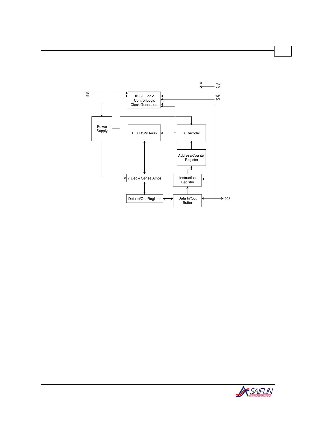
Figure 1. SA24C1024 Block Diagram .............................. 4
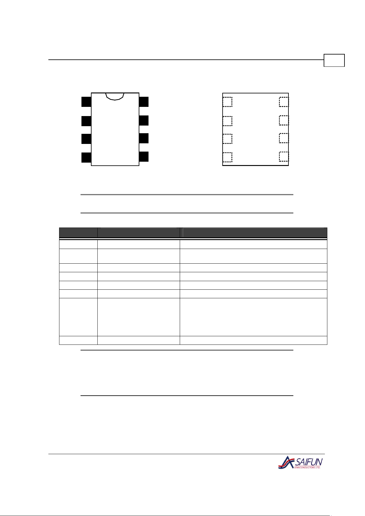
Figure 2. SO Package (MW), Dual Inline (N) – Top View 5
Figure 3. Leadless Package (MLF) – Top View ............... 5
Figure 4. SA24C1024 Ordering Information..................... 6
Figure 5. AC Testing Input/Output Waveforms ................ 9
Figure 6. Bus Timing..................................................... 10
Figure 7. Write Cycle Timing......................................... 11
Figure 8. Typical System Configuration ......................... 11
Figure 9. Slave Address ................................................ 12
Figure 10. Data Validity ................................................. 17
Figure 11. START and STOP Definition ........................ 17
Figure 12. Acknowledge Response from Receiver ........ 17
Figure 13. Byte Write .................................................... 19
Figure 14. Page Write ................................................... 19
Figure 15. Current Address Read.................................. 21
Figure 16. Random Read .............................................. 21
Figure 17. Sequential Read........................................... 21
Figure 18. Data Transfer ............................................... 22
Figure 19. A Complete HS Mode Transfer..................... 23
Figure 20. 8-pin Molded Small Outline Package (MW8),
Package Number M08D ...................................... 24
Figure 21. Molded Dual-in-Line Package (N), Package
Number N08E...................................................... 25
Figure 22. 8-pin MLF Leadless Package ....................... 26
List of Tables
Table 1. Pin Names......................................................... 5
Table 2. Write Protection Truth Table............................ 14
SA24C1024 Datasheet
SAIFUN
4
Block Diagram
Figure 1. SA24C1024 Block Diagram
SA24C1024 Datasheet
SAIFUN
5
Connection Diagrams
SA24C1024
1
2
3
4
8
7
6
5
NC
A1
NC
V
SS
V
CC
WP
SCL
SDA
SA24C1024
1
2
3
4
8
7
6
5
NC
A1
NC
V
SS
V
CC
SCL
SDA
Figure 2. SO Package (MW), Dual Inline (N) – Top
View
Figure 3. Leadless Package (MLF) – Top View
Note:
For more details, refer to package number N08E and M08D.
Table 1. Pin Names
Symbol
Pin Name Description
NC Not Connected
A1
Device Select Address Input
Pin
Has an internal "weak" pulldown, and assumes logic LOW
when left unconnected.
NC Not Connected
VSS Device Ground Input Pin
SDA IIC Data Input/Output Pin Open Collector/Drain type.
SCL IIC Clock Input Pin
WP
Write Protect
Has an internal "weak" pulldown, and assumes logic LOW
when left unconnected.
When LOW, writing is allowed to the memory array.
When HIGH, writing is not allowed to the memory array, as
defined in Write Protect (WP), page 14.
VCC Device Power Input Pin 2.7 V to 3.6 V
Note:
No A2 or A0 pins (Pins 2 and 3) are provided, and are instead treated as Not
Connected. Internal address comparison assumes pin A2 to be 0, and so the
command code should have its corresponding A2 bit set to 0 as well. The
command code should also have its corresponding A0 bit set to add16 (MSB
address bit).

SA24C1024 Datasheet
SAIFUN
6
Ordering Information
LZXXC24SA Letter
L
LZ
1024
C
24
SA
Interface
Density
Voltage Operating Range
Description
2.7 V to 3.6 V
2.7 V to 3.6 V
< 0.7 µA Standby Current
1 Mb with Write Protect
CMOS EEPROM
Technology
IIC - 2 Wire
Saifun Non-Volatile
Memory
X
Blank
X
Tube
Tape and Reel
PP
Package
N
MW
MF
8-pin DIP
8-pin SOIC (200 mil)
8-lead MLF
F
Blank
F
Non-lead Free
Lead-free Leads
E
Blank
E
Temp. Range
0 to 70 C
-40 to +85 C
o
o
Figure 4. SA24C1024 Ordering Information

SA24C1024 Datasheet
SAIFUN
7
Product Specifications
Absolute Maximum Ratings Operating Conditions
Ambient Storage Temperature
–65 °C to +150 °C
All Input or Output Voltages with
Respect to Ground
4.5 V to -0.3 V
Lead Temperature
(Soldering, 10 seconds)
+300 °C
ESD Rating 2000 V min.
ESD/Latch up Specification (JEDEC 8 Spec)
Human Body Model Minimum 2 KV
Machine Model Minimum 500 V
Latch up
100 mA on all pins, +125 °C
Operating Conditions
Ambient Operating Temperature:
•= SA24C1024
•= SA24C1024E
0°C to +70°C
–40°C to +85°C
Positive Power Supply:
•= SA24C1024
•= SA24C1024LZ
2.7 V to 3.6 V
2.7 V to 3.6 V
SA24C1024 Datasheet
SAIFUN
8
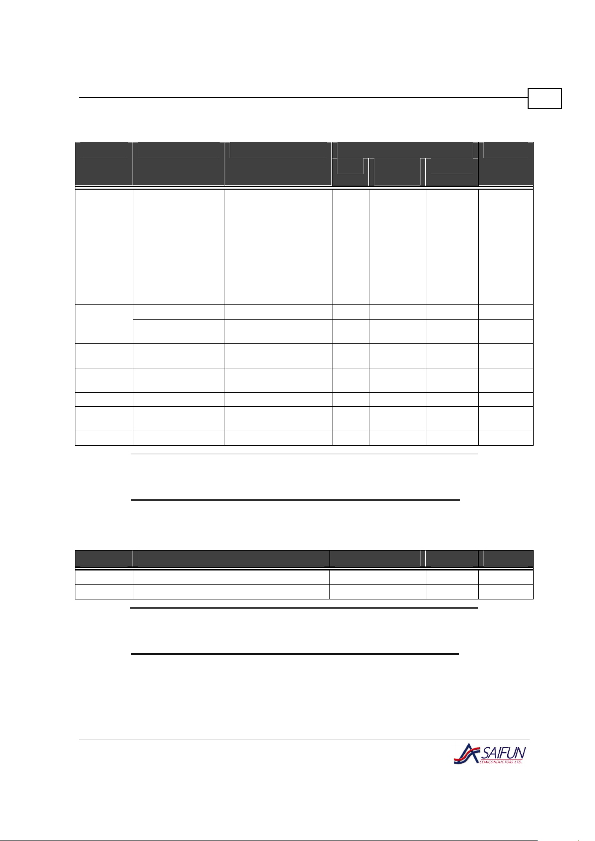
VCC (2.7 V to 3.6 V) DC Electrical Characteristics
Limits Symbol Parameter Test Conditions
Min Typ
(Notes)
Max
Units
f
SCL
= 100 kHz (Read) 2 3 mA
f
SCL
= 100 kHz (Write) 8 11 mA
f
SCL
= 400 KHZ (Read) 2 3 mA
f
SCL
= 400 kHz (Write) 8 11 mA
f
SCL
= 1.7 MHz (Read) 5 7 mA
f
SCL
= 1.7 MHz (Write) 8 11 mA
f
SCL
= 3.4 MHz (Read)
5 7 mA
I
CCA
Active Power Supply
Current
f
SCL
= 3.4 MHz (Write)
8 11 mA
ISB Standby Current (L) VIN = GND or V
CC
0.5 1
µA
Standby Current
(LZ)
VIN = GND or VCC 0.2 0.7
µA=
IIL Input Leakage
Current
VIN = GND to V
CC
0.1 1
µA
IOL Output Leakage
Current
V
OUT
= GND to V
CC
0.1 1
µA
VIL Input Low Voltage
-0.3 VCC x 0.3 V
V
IH
Input High Voltage
VCC *
0.7
V
CC
+ 0.5 V
V
OL
Output Low Voltage I
OL
= 3 mA
0.4 V
Notes:
(1) Typical values are TA = +25 °C and nominal supply voltage of 3 V.
(2) Write frequency is 50 Hz.
Capacitance
T
A
= +25 °C, f = 100/400 kHz/1.7 MHz/3.4 MHz, V
CC
= 3V (see note 2)
Symbol Test Conditions Max Units
C
I/O
Input/Output Capacitance (SDA) V
I/O
= 0 V 8 pF
CIN Input Capacitance (A0, A1, A2, SCL) V
IN
= 0 V 6 pF
Notes:
(1) This parameter is periodically sampled and not 100% tested.
(2) Typical values are T
A
= +25 °C and nominal supply voltage of 3 V.
SA24C1024 Datasheet
SAIFUN
9
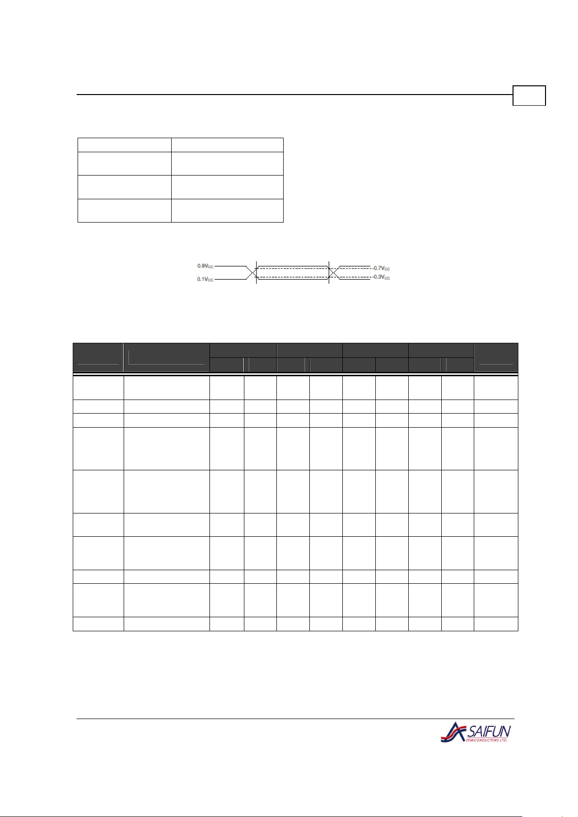
AC Test Conditions
Input Pulse Levels VCC * 0.1 to VCC * 0.9
Input Rise and Fall
Times
10 ns
Input & Output Timing
Levels
VCC * 0.3 to VCC * 0.7
Output Load
1 TTL Gate and CL = 100
pF
AC Testing Input/Output Waveforms
Figure 5. AC Testing Input/Output Waveforms
AC Characteristics (VCC 2.7 V – 3.6 V)
100 kHz 400 kHz 1.7 MHz 3.4 MHz
Symbol Parameter
Min Max Min Max Min Max Min Max
Units
f
SCL
SCL Clock
Frequency
100
400
1700 3400
kHz
t
LOW
Clock Low Period 4700 1300 320 160 ns
t
HIGH
Clock High Period 4000 600 120 60 ns
tSU:STA
Start Condition
Setup Time (for a
repeated START
condition)
4700 600
160 160
ns
t
HD:STA
Start Condition
Hold Time (for a
repeated START
condition)
4000 600
160 160
ns
t
SU:STO
Stop Condition
Setup Time
4000 600
160 160
ns
t
RDA
SDA Rise Time
(depend on
external pullup)
1000 300 20 170 10 85 ns
t
FDA
SDA Fall Time 300 300 20 170 10 85 ns
t
RCL
SCL Rise Time
(depend on
external pullup)
1000 300 20 80 10 40 ns
t
FCL
SCL Fall Time 300 300 20 80 10 40 ns
 Loading...