

- Industrial interface
TECHNICAL NOTE
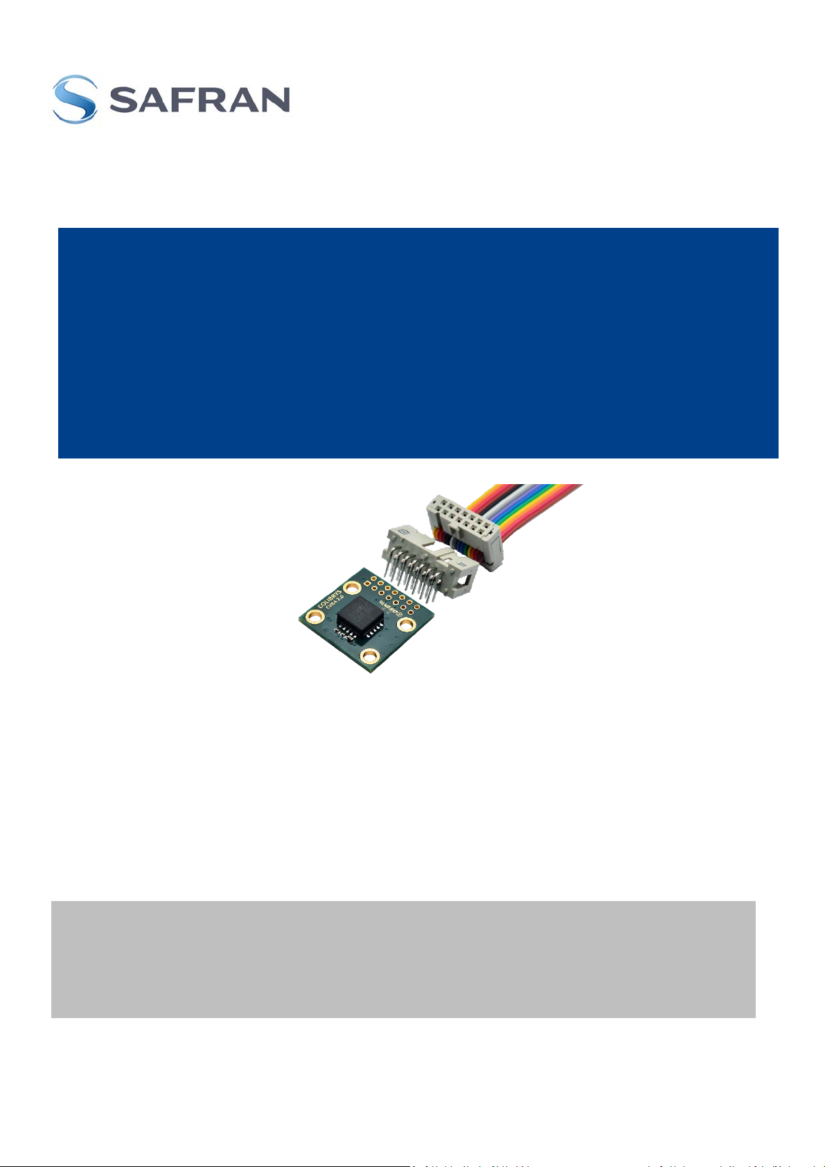
VS1000: Evaluation Kit EVBA_2.0
EVBA_2.0 – is a “plug and play” Evalu ation Kit for Safran Colibrys VS1000 accelerometers line.
To facilitate the integrat ion in user environment and easil y verify the excellent performanc es of VS1000 sensors,
EVBA_2.0 integrates a VS1000 sensor with the user specified range, an ultra-low-noise, high-accuracy 3.3V voltage
reference, the decoupling capacitors and output buffers.
Features:
- Low noise power supply management converting +5V to 3.3V
- Output signal conditioning:
buffers to enable the use of long lines between the sensor and the user electronic
low-pass filters with a cutting frequency
- Easy integration into system: 4 fixing holes
Contents
1 EVBA_2.0 description: ......................................................................................................................................... 2
2 Evaluation board function .................................................................................................................................... 4
3 Operation ............................................................................................................................................................. 7
4 Ordering Information ............................................................................................................................................ 9
5 Disclaimer ............................................................................................................................................................ 9
VS1000: Evaluation Kit EVBA_2.0
Document number 30N.EVBA_2.0.A
Document revision V1.0
Date of revision 06 September 2016
Note Safran Colibrys reserves the right to change these data without notice
Safran Colibrys reserves the right to change these data without notice
by electrostatic discharge (ESD). Handle with appropriate precautions and
Pin Nr
Pin name
Connector
Description
1
VTemp_f
J1
Temperature sensor analog output (buffered)
2
VDD_s
J1
+3.3 VDC reference voltage sens e output (not buffered)
3
OUTN_f
J1
Negative differential output (buffered)
4
V
MID
J1
Internal ASIC reference voltage. For decoupling capacitors only
5
OUTP_f
J1
Positive differential output (buffered)
6
VSS (0 V)
J1
Must be connected to ground plane (GND)
7
Vout_SE
J1
Single output acceleration (Vout_SE = OUTP - OUTN) (buffered)
8
Vp (+5V)
J1
Power supply 5.0VDC – 5.5VDC
9
VSS (0 V)
J1
Must be connected to ground plane (GND)
10
VSS (0 V)
J1
Must be connected to ground plane (GND)
11
ERR
J1
Error signal (output, active high)
12
ST
J1
Self-test activation (input, active high)
13
POR
J1
Power-on Reset signal (output, active high)
14
RESET
J1
System reset signal (input, active low)
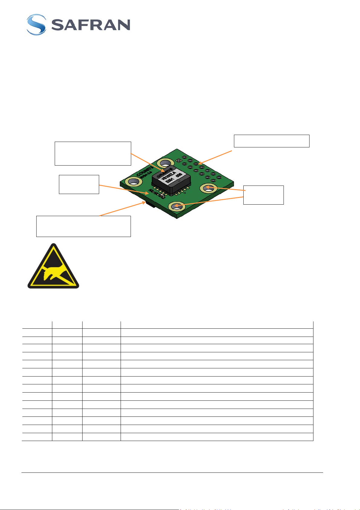
Accelerometer VS1000
Decoupling
capacitors
Connecting holes “J1”
Ø3.4mm
fixing hole
Proximity electronics, with
TECHNICAL NOTE
1 EVBA_2.0 description:
1.1 General overview
The EVBA_2.0 is a Kit containing 3 components:
- 1 analog evaluatio n board with soldered V S1000 of c orrespond ing G range. Evaluation board contains
electronic circuits to achieve a preliminary signal conditioning
- 1 * header connector “J1” with 14 pins (to be soldered onto the EVBA dedicated pads)
- 1 * mating connector (14 pins) including 13 cm length signal cable ribbon
The EVBA_2.0 is protected from outside atmospheric condition effects (temperature, humidity) by a vacuum
sealed electrostatic conductive plastic bag
power supply and buffers
Note: MEMS accelerom eter and electro nic cir cuits on t he EVB A can be dam aged
placement should be done in accordance with strict ESD control
Please check the integrity of the plastic bag and report if any damage or if the bag
is open on arrival.
1.2 Interface Pinout
The Table 1 below describes the pin name and interface for the connecting pads J1:
(1)
Note 1: this pin should be left unconnected.
Table 1: Interface Pinout
Safran Colibrys SA
Av. des Sciences 13 – 1400 Yverdon-les-Bains - Switzerland T +41 58 100 5000
www.safran-colibrys.com page 2 F +41 58 100 5001
30N.EVBA V2.10.16

1 2 13
14
TECHNICAL NOTE
1.3 Electrical connections
It is the user choice to mount Header connector (Figure 1) on J1 connecting pads or to solder the signal wires
directly on the EVBA board. The size of the soldering hole are of 0.8mm, so wires up to a conductor area of
0.5mm2 or AWG21 are suitable. The wires or the Mating connector (Figure 2) will ideally be hand soldered
using a PB free solder with the appropriate flux.
Note: Connector J1 is a 14 Positions Header, Shrouded Connector 0.100" (2.54mm) Through Hole, Right Angle
This connector is delivered unsoldered to the evaluation board. The user is free to use it or to solder any
connection directly on the board.
Figure 1: Connector J1 Figure 2: Mating connector (14 pins)
1.4 Mechanical dimensions
The mechanical layout of the evaluation board is shown in Figure 3. All components are soldered on the top
and bottom surface and the board can be mounted using the 4 x Ø3.40 mm through holes:
Note: This is for the VS1002, other range looks like same
Figure 3: Mechanical Dimensions [mm] showing a VS1002
Safran Colibrys SA
Av. des Sciences 13 – 1400 Yverdon-les-Bains - Switzerland T +41 58 100 5000
www.safran-colibrys.com page 3 F +41 58 100 5001
30N.EVBA V2.10.16

TECHNICAL NOTE
2 Evaluation board function
To fac ilitate the integration in an user environment a nd easily verify the excel lent performances of the Safran
Colibrys VS1000 s er ie sensors, the p lu g a nd pl a y board EVBA_2.0 integrates one VS1 000 s ensor with the user
specified range, an ultra-low-noise, high-accur ac y 3.3V voltage reference, the dec oupling ca pacit ors and out put
buffers as shown in Figure 4. The board will powered by a single +5V
2.1 Normal operation (recommended)
Optimal acceleration m easurem ents are ach ieved by using the diff erential buff ered signal outputs OUTP_f and
OUTN_f.
2.2 Optional operation
If user application requires a unipolar signal, a single-ended buffered output Vout_SE is provided as well.
2.3 Block Diagram
The Block diagram of the EVBA2.0 is given below. The sensor implemented is represented by the green marked
zone. The VS1000 sensor signal outputs are linked to a unity gain buffer via a 1
The Output of the unity gain buffer is then connected to the dedicated pins of J1. The board +5.0V power supply
is connected to VP and an Ultra-Low-N oise, High-Accuracy 3.3V Volt age Reference generates the necessary
+3.30 VDD voltage. The capacitors C1, C2 and C3 forms the decoupling elements for the ASIC reference voltage
Vmid. Note that this voltage level is also linked to J1. That pin must be left open for normal operation.
The single ended output signal Vout_SE expresses the relation described at §2.8
power supply.
DC
st
order low pass filter (fc=16kHz).
Figure 4: Functional Diagram EVBA2.0
Safran Colibrys SA
Av. des Sciences 13 – 1400 Yverdon-les-Bains - Switzerland T +41 58 100 5000
www.safran-colibrys.com page 4 F +41 58 100 5001
30N.EVBA V2.10.16

2.4 Electrical Schema
The corresponding detailed electrical schema is given below.
TECHNICAL NOTE
Figure 5: EVBA Elect ro n ic c ir c uit
2.5 Power Supply
The EVBA power supply is set for +5.0V
(pin8 of J1) and the 0VDC must be connected to all VSS pins of J1 (pin
DC
6, pin 9, pin10).
The VS1000 series accelerometers require a +3.30VDC power supply named Vdd. The sensor outputs are
ratiometric to that Vdd voltage level. This could directly impact the acceleromet er bias, scale factor, noise or
thermal perform ance. Therefore, a low-noise, high-stability and lo w-thermal drift Vdd po wer supply has been
implemented on the board using an Ultra-Low-Noise, High-Accuracy 3.3V Voltage Reference type ADR4533.
The Sensor Vdd line (+3.30V
) is als o connec ted to PIN 2 of the J1 a nd can be then used as an out put si gnal
DC
(VDD_S) in order to compens ate any variatio n on the power suppl y voltage that may im pact the accelerometer
signal (ratiometric output).
The voltage Vmid sets to a le vel of 0. 5 x Vdd and is a voltage required b y the ASI C of the sensor. F or a norm al
operation of the sensor th is line should be left op en. Checking the level sha ll be only reserved and lim ited for
debug purposes. Any impedance c onnec ted to that line c ould dir ectl y im pac t the st abilit y, bias, s cale f actor an d
noise figure of the VS1000 series sensors.
Safran Colibrys SA
Av. des Sciences 13 – 1400 Yverdon-les-Bains - Switzerland T +41 58 100 5000
www.safran-colibrys.com page 5 F +41 58 100 5001
30N.EVBA V2.10.16

TECHNICAL NOTE
2.6 Accelerom eter sen so r
The sensor block is composed of the VS1000 accelerometer and three capacitors C1 (10 µF), C2 (1 µF) and C3
(1 µF). These capacitors are required as decoupling capacitors and for a proper sensor startup. They are
mandatory for the pr oper operation and full perf ormance of the accelerometer. T hey are located as close as
possible to the VS1000 package on the printed circuit board.
2.7 Output signal conditioning
The analog acceler at ion s ignal ou tput lines (OutN, O ut P) req uir e a h igh impedance load in or der not to degrade
the signal characteristic. To drive long signal lines between the EVBA and the user electronic, buffers have been
implemented on the EVBA. Additionally the Temperature analog output signal is also buffered.
The buffers are implem ented using a Zero-Drif t, Single-Sup ply, Rail-to-R ail Input/Output Operatio nal Amp lifiers
type AD8574.
The operational am plifiers U3A, U3B and U3C are configured as vo ltage f ollower (gain =1) and are prec eded by
low-pass filters R8/C8, R7/C7 and R6/C6 respectively introducing a cutting frequency of 16 kHz. The attenuation
at 1500Hz is less than 0.5%, allowing the use of the full bandwidth of the sensor.
The resistors R15, R14 an d R13 (all of 100 Ω) are connected t o the buf fer output reduc e the lo op phas e shif t at
high frequency when driving a capacitive load (ie the cable link between the EVBA and the Electronic system).
2.8 Differential to Single Output
Safran Colibrys’s VS1000 series provide a differential output for the sensed acceleration. The EVBA implements
a differential to single en ded m ode c onverter built arou nd the four th O P am plifier of the AD8574 ( U3D). A s et of
matched resistances is used to divide the voltages and add an offset to avoid saturation of the amplifier:
−
_
=
_
_
2
Note:
- The scale factor of the single ended output is only half that of the differential output.
- The common mode noise is not canceled when using a single ended output.
2.9 Temperature sensing
Each Safran Colibrys VS1000 accelerometer integrate an internal temperature sensor. The output voltage
Vtemp_f buffer ed by OPAMP U3B (u nity gain) to PIN1 of J 1 gives a voltage pro portional to t he internal sensor
temperature and can be u sed to achieve additional com pensation of the measured acceleration to ob tain the
optimum readouts.
The temperature is then given by the function
= 1.23 − 0.004 ( −
+
2
)
Safran Colibrys SA
Av. des Sciences 13 – 1400 Yverdon-les-Bains - Switzerland T +41 58 100 5000
www.safran-colibrys.com page 6 F +41 58 100 5001
30N.EVBA V2.10.16

TECHNICAL NOTE
2.10 Bill of material (BOM)
The following table lists all components used for the presented design:
Component Value Function
U1 VS1000 Safran Colibrys Accelerometer
U2 ADR4533 3V3 Voltage Reference – Analog Devices ADR4533BRZ
U3 AD8574 Quad Operational Amplifier – Analog Devices AD8574ARZ
R1, R2, R3, R4 10 kΩ Voltage divider – 0402 resistor
R5 20 kΩ Voltage divider – 0402 resistor
R6, R7, R8 100 kΩ Low pass filter – 0402 resistor
R9, R10 5 kΩ Voltage divider – 0402 resistor
R11, R12 40 kΩ Voltage divider – 0603 resistor
R13, R14, R15, R16 100 Ω Output load – 0402 resistor
C1 10 µF Decoupling – 0603 capacitor
C2, C3, C4 1 µF Decoupling – 0402 capacitor
C5 100 nF Decoupling – 0402 capacitor
C6, C7, C8 100 pF Low pass filter – 0402 capacitor
J1 HEADER 7X2 Connector (if required*)
*The wires may also be soldered directly on the board.
Table 2: Bill of material
3 Operation
Handle with appropriate precautions and be done in accordance with strict ESD control.
It is the user choice to use the connector provided or to solder the signal wire lines
directly on the board. In both situation please follow the proper soldering process. Hand
soldering is recommended.
3.1 Power Up
Once the cabling done the EVBA can be powered up by applying the VP voltage level. The current consumption
and the reference voltage V
Parameter Designation [unit] Typical
Sensor +3.30V power supply VDD [VDC]
Board current consumption IP [mADC]
shall be:
DD
3.30
7.14
Safran Colibrys SA
Av. des Sciences 13 – 1400 Yverdon-les-Bains - Switzerland T +41 58 100 5000
www.safran-colibrys.com page 7 F +41 58 100 5001
30N.EVBA V2.10.16

Single-ended
VOUT_SE
J1 / Pin#
Signal
Designation
12
ST
Self-test activation, active high
14
RESET
System reset signal, active low
TECHNICAL NOTE
3.2 Outputs
With the EVBA board placed horizontal in a quite environment will expose the sensor to an acceleration of 1g.
The corresponding level of the signals OUTP_f, OUTN_f and Vout_SE settles proportional to the range and
scale factor of the VS1000 mounted. The available ranges are ± 2g, 5g, 10g, 30g, 100g and 200g.
The typical readouts are at 1g acceleration:
Parameter
OUTP OUTP [VDC]
OUTN OUTN [VDC]
output
With the EVBA operated in an ambient temperature of +25°C ± 3°C the Vtemp-f signal on J1/1 shall read:
Designation
[unit]
[VDC]
2g 5g 10g 30g 50g 100g 200g
2.325 1.920 1.785 1.695 1.677 1.663 1.657
0.975 1.380 1.515 1.605 1.623 1.636 1.643
2.325 1.920 1.785 1.695 1.677 1.663 1.657
Parameter Designation [unit] Typical
Typical
Vtemp buffered Vtemp_f [VDC]
The VS1000 accelerometer provides logic output signals:
1.210
Parameter Designation [unit] Typical
Error signal (flag) ERR [VDC]
Power-on Reset signal (flag) POR [VDC]
Vss
Vdd
3.3 Logic signals
Some functionalities can be controlled by applied logical signals according to the Table 3.
They all are referenced to the VS1000 Vdd (+3.3V
) voltage level and proper
DC
interfacing is required. A Logic HIGH level corres ponds to the Vd d voltage level and a
logic LOW level to the Vss voltage level.
Table 3
For the detailed function and effects of these signals please refer to the Datasheet of the VS1000 sensor.
Safran Colibrys SA
Av. des Sciences 13 – 1400 Yverdon-les-Bains - Switzerland T +41 58 100 5000
www.safran-colibrys.com page 8 F +41 58 100 5001
30N.EVBA V2.10.16

Range [g]
Designation
Part Number
±2
EVBA_2.0_VS1002.A
37628071
±5
EVBA_2.0_VS1005.A
37623081
±10
EVBA_2.0_VS1010.A
37625033
±30
EVBA_2.0_VS1030.A
37628084
±50
EVBA_2.0_VS1050.A
37629043
±100
EVBA_2.0_VS1100.A
37629061
±200
EVBA_2.0_VS1200.A
37629081
TECHNICAL NOTE
4 Ordering Information
The user will have to select the appropriate sensor range for his application (see VS1000 family data sheet) and
then order the corr esponding EVB A version. Table 4 sho ws the range, Designat ion and Part num ber for each
available EVBAs.:
Table 4: EVBA ordering number
5 Disclaimer
EVBA_2.0_VS1000 evaluation kit is only intended for device evaluation, not for production purposes.
Safran Colibrys SA
Av. des Sciences 13 – 1400 Yverdon-les-Bains - Switzerland T +41 58 100 5000
www.safran-colibrys.com page 9 F +41 58 100 5001
30N.EVBA V2.10.16
 Loading...