

Page 1

®
R&S
R
T‑ZD10/20/30
Active Differential Probe
®
R&S
RT‑ZA15
External Attenuator
User Manual
(>:]À2)
1410455002
Version 05
User Manual
Page 2

This user manual describes the following R&S®R
attenuators:
●
R&S®RT-ZD10 (1410.4715.02)
●
R&S®RT-ZD20 (1410.4409.02)
●
R&S®RT-ZD30 (1410.4609.02)
●
R&S®RT-ZA15 (1410.4744.02)
T-ZD models and external
© 2019 Rohde & Schwarz GmbH & Co. KG
Mühldorfstr
Phone: +49 89 41 29 - 0
Fax: +49 89 41 29 12 164
Email: info@rohde-schwarz.com
Internet: www.rohde-schwarz.com
Subject to change – Data without tolerance limits is not binding.
R&S® is a registered trademark of Rohde & Schwarz GmbH & Co. KG.
Trade names are trademarks of the owners.
1410.4550.02 | Version 05 | R&S®RT‑ZD10/20/30
Throughout this manual, products from Rohde & Schwarz are indicated without the ® symbol and without
product type numbers, e.g. R&S®RT-RT-ZD10/20/30 is indicated as R&S RT-ZD10/20/30.
. 15, 81671 München, Germany
Page 3

R&S®RT‑ZD10/20/30
Contents
1
Product Description.............................................................. 5
1.1 Key Features and Key Characteristics............................................... 5
1.2 Unpacking..............................................................................................7
1.3 Description of the Probe...................................................................... 8
1.4 Accessories and Items......................................................................... 9
2 Putting into Operation.........................................................15
2.1 Connecting the Probe to the Oscilloscope...................................... 16
2.2 Identification of the Probe..................................................................17
Contents
2.3 Using the Probe.................................................................................. 17
2.4 Offset Compensation..........................................................................18
3 R&S RT‑ZA15 External Attenuator..................................... 23
3.1 Key Characteristics............................................................................ 23
3.2 Description.......................................................................................... 24
3.3 Inserting the Probe............................................................................. 24
3.4 Adjusting............................................................................................. 25
4 Connecting the Probe to the DUT...................................... 30
5 Characteristics of Differential Probes............................... 36
5.1 Common Mode Rejection Ratio (CMRR)...........................................37
5.2 Dynamic Range and Operating Voltage Window............................. 38
5.3 Ground Connection............................................................................ 39
6 Measurement Principles..................................................... 40
6.1 Signal Integrity of the Transferred Signal.........................................42
6.2 Signal Loading of the Input Signal....................................................46
6.3 Probing Philosophy............................................................................ 49
3User Manual 1410.4550.02 ─ 05
Page 4

R&S®RT‑ZD10/20/30
Contents
7 Maintenance and Service....................................................51
7.1
Cleaning...............................................................................................51
7.2 Contacting Customer Support...........................................................51
7.3 Returning for Servicing...................................................................... 52
7.4 Calibration Interval............................................................................. 53
7.5 Discarding the Product...................................................................... 53
7.6 Spare Parts.......................................................................................... 53
8 Functional Check.................................................................56
Index..................................................................................... 57
4User Manual 1410.4550.02 ─ 05
Page 5

R&S®RT‑ZD10/20/30
Key Features and Key Characteristics
Product Description
1 Product Description
1.1 Key Features and Key Characteristics
The R&S RT‑ZD10/20/30 is a differential probe with high input impedance. It is
used for differential voltage measurements from DC to 1.0 GHz, 1.5 GHz, and
3 GHz, respectively.
Differential probes can be used for single-ended and differential applications.
They are equipped with two high-impedance inputs and can measure the voltage
between any two test points. Unlike using single-ended probes, there is no need
to ensure that one of the test points is always at ground potential.
The comprehensive accessory set allows this probe to be connected to a wide
variety of devices under test (DUT). Provided with special features such as the
R&S ProbeMeter and the micro button, the R&S RT‑ZD10/20/30 is designed to
meet tomorrow's challenges in probing.
The external attenuator R&S RT‑ZA15 can be used to extend the input voltage
range of the R&S RT‑ZD10/20/30. It is supplied with the R&S RT‑ZD10 and is
available as optional accessory for the R&S RT‑ZD20/30.
The probe is equipped with theRohde & Schwarz probe interface. It can be connected to any Rohde & Schwarz instrument that is compatible with this interface.
When connected to the front panel, the probe is controlled by the oscilloscope's
software. Supported oscilloscopes are listed in the data sheet.
Using a specially developed adapter (see Chapter 1.4.2, "Optional Accessories",
on page 13), the probe can also be connected to any other base unit.
5User Manual 1410.4550.02 ─ 05
Page 6

R&S®RT‑ZD10/20/30
Key Features and Key Characteristics
1.1.1 Key Characteristics
The key characteristics of the probe are the following:
Bandwidth DC to 1.0 GHz (R&S RT-ZD10)
DC to 1.5 GHz (R&S R
DC to 3.0 GHz (R&S RT-ZD30)
T-ZD20)
Product Description
Dynamic range
(differential input)
Operating voltage window
(each pin to GND)
Maximum non-destructive input voltage ±30 V
Diff. input resistance 1 MΩ
Diff. input capacitance 0.6 pF
R&S ProbeMeter, measurement error <0.1 %
Extremely low zero and gain errors throughout the entire temperature range, no significant temperature drift
Micro button
Rohde & Schwarz probe interface
±5 V with ±5 V offset capability
10 V AC (Vpp)
±8 V with ±22 V common mode offset capability
Available for R&S RT‑ZD10/20/30 probes with serial
number ≥ 200000
Between each signal pin and ground
1.1.2 Key Features
Micro button
The micro button at the probe head can remotely control dif
ferent functions on the
base unit. The assigned function is configured via the base unit.
For details, see Chapter 2.3.2, "Micro Button", on page 18.
R&S ProbeMeter
The R&S ProbeMeter measures the DC voltage of the input signal directly at the
probe tip. It provides a continuous high-precision DC voltage measurement that is
independent of the settings of the oscilloscope and runs in parallel to the time
domain measurement. If activated on the base unit, the measured value is displayed on the screen of the Rohde & Schwarz oscilloscope.
6User Manual 1410.4550.02 ─ 05
Page 7

R&S®RT‑ZD10/20/30
Product Description
Unpacking
The R&S ProbeMeter simultaneously measures both differential and common
mode DC voltages.
For details, see Chapter 2.4.3, "R&S ProbeMeter", on page 21.
Data memory
The probe has an integrated data memory
, containing the individual probe correc-
tion parameters (e.g. gain, delay, offset). These parameters are read out and processed by the Rohde & Schwarz oscilloscope. As a result, the probe offers a high
degree of accuracy, and additional calibration procedures are not required.
1.2 Unpacking
The carrying case contains the following items:
●
R&S R
●
Carrying case
●
Accessory boxes
●
User manual
●
R&S RT‑ZD10/20/30 data sheet
●
Calibration certificate
●
Documentation of calibration values (if
ordered)
●
R&S RT-ZA15 external attenuator (only
with R&S RT-ZD10)
T‑ZD10/20/30 differential probe
1.2.1 Inspecting the Contents
●
Inspect the package for damage.
Keep the package and the cushioning material until the contents have been
checked for completeness and the device has been tested.
If the packaging material shows any signs of stress, notify the carrier and your
Rohde & Schwarz service center
for inspection.
●
Inspect the probe.
If there is any damage or defect, or if the R&S RT‑ZD10/20/30 differential
probe does not operate properly, notify your Rohde & Schwarz service center.
. Keep the package and cushioning material
7User Manual 1410.4550.02 ─ 05
Page 8

R&S®RT‑ZD10/20/30
Product Description
Description of the Probe
●
Inspect the accessories.
If the contents are incomplete or damaged, notify your Rohde & Schwarz service center
.
Accessories supplied with the device are listed in Chapter 1.4.1, "Accessories
Supplied", on page 10.
1.3 Description of the Probe
The probe consists of the probe head for connection to the DUT, the probe box
for connection to the oscilloscope, and the probe cable.
1.3.1 Probe Head
The small and lightweight probe head is designed for easy handling and high-performance measurements. The probe head is used for connecting the probe and
the DUT
. Different accessories for the signal and ground sockets allow the probe
head to be connected to a wide range of DUTs.
(1) Positive signal socket
(2) Negative signal socket
(3) Ground socket
(4) Micro button
The accessories supplied for the probe head
sockets are listed in Chapter 1.4.1, "Accesso-
ries Supplied", on page 10
Signal and ground sockets are compatible with
0.64 mm (25 mil) square pins and 0.6 mm to
0.8 mm (24 mil to 35 mil) round pins.
Spacing of signal sockets: 5.08 mm (200 mil).
.
8User Manual 1410.4550.02 ─ 05
Page 9

R&S®RT‑ZD10/20/30
Product Description
Accessories and Items
1.3.2 Probe Box
The probe box connects the probe and the oscilloscope via the Rohde & Schwarz
probe interface. The Rohde & Schwarz probe interface contains a male precision
7 mm (276 mil) BNC connector and six pogo pin connectors. This interface provides the required supply voltage and is also used to transmit analog signals and
digital data simultaneously
erated in the probe box. This approach ensures that it will be possible to operate
future probes on any base unit that features a Rohde & Schwarz probe interface.
. All the analog voltages required by the probe are gen-
(1) Rohde & Schwarz probe interface with
7 mm (276 mil) coaxial connector and 6 pogo
pins
(2) Release knob
Connect the R&S R
T‑ZD10/20/30 only to an instrument with Rohde & Schwarz
probe interface. Never connect it to a usual BNC jack. Although the 7 mm coaxial
connector looks like a standard BNC connector, it is constructed differently and
does not fit to the standard BNC jack. The interface of the R&S RT‑ZD10/20/30
can withstand a higher frequency limit.
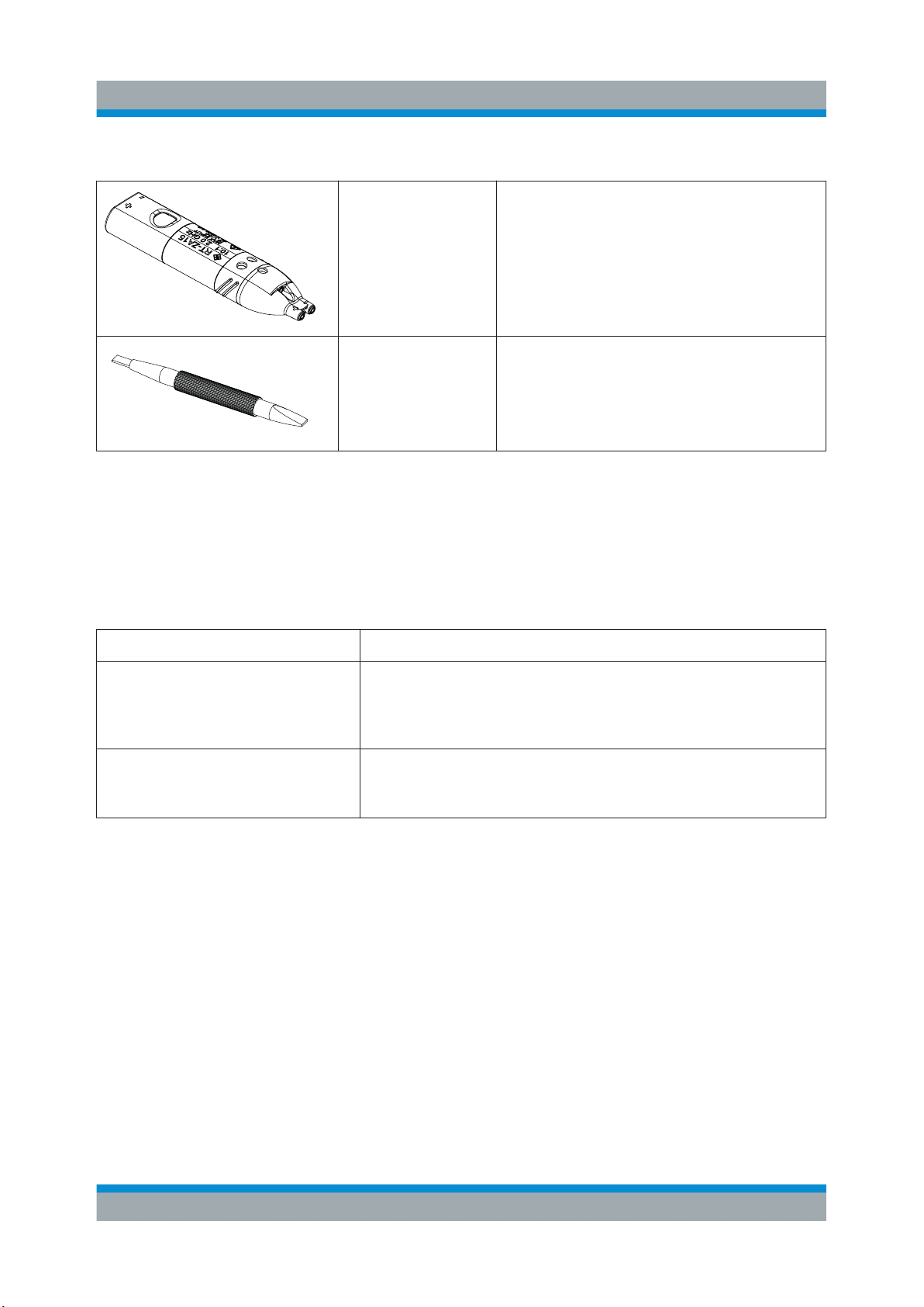
1.4 Accessories and Items
The figure below shows all accessories that are available for the
R&S RT‑ZD10/20/30 differential probe.
9User Manual 1410.4550.02 ─ 05
Page 10

R&S®RT‑ZD10/20/30
Product Description
Accessories and Items
RT-ZA15 External Attenuator
Figure 1-1: Available accessories
1.4.1 Accessories Supplied
The following table shows the accessories supplied with the R&S R
differential probe.
T‑ZD10/20/30
10User Manual 1410.4550.02 ─ 05
Page 11

R&S®RT‑ZD10/20/30
Table 1-1: Accessories supplied
Item Quantity Description
Product Description
Accessories and Items
10 Signal pin, solder-in
4 Signal pin, variable spacing
1 Browser adapter
2 Adapter, square pin
1
1
1
1
2 Lead, 6 cm / 2.4 in
Flex adapter, solder-in,
4 cm / 1.6 in
10 cm / 3.9 in
Flex adapter, square pin,
4 cm / 1.6 in
10 cm / 3.9 in
11User Manual 1410.4550.02 ─ 05
Page 12

R&S®RT‑ZD10/20/30
Item Quantity Description
Product Description
Accessories and Items
1 Lead, 15 cm / 5.9 in
2 Mini clip
2 Micro clip
1 Marker band kit
1
(only with R&S R
(only with R&S RT‑ZD10)
T‑ZD10)
1
1
External attenuator
Adjustment tool
Carrying case with foam
inlay
12User Manual 1410.4550.02 ─ 05
Page 13

R&S®RT‑ZD10/20/30
Product Description
Accessories and Items
For a list of spare parts, see Chapter 7.6, "Spare Parts", on page 53.
1.4.2 Optional Accessories
If the delivered accessories do not meet individual customer requirements,
Rohde & Schwarz offers different accessory sets for sale. The order numbers are
provided in the data sheet.
RT‑
Table 1-2: R&S
Item Quantity Description
Mini clip 10 Contains mini clips.
Table 1-3: R&S RT‑ZA5 micro clips
Item Quantity Description
Micro clip 4 Contains micro clips.
ZA4 mini clips
RT‑
Table 1-4: R&S
Item Quantity Description
Lead, 6 cm / 2.4 in
Lead, 15 cm / 5.9 in
Table 1-5: R&S
Item Quantity Description
Signal pin, solder-in
Signal pin, variable spacing
Browser adapter
Browser adapter, rigid / pogo
Adapter, square pin
Table 1-6: R&S
ZA6 lead set
RT‑
ZA7 differential pin set
, pogo / pogo
RT‑
ZA9 probe box to N / USB adapter
The adapter can be used to connect the
R&S R
oscilloscope or any other measurement instrument
(e.g. a network or spectrum analyzer).
Using the USB interface of the adapter, the probe
can be powered and controlled from any conventional PC.
5
5
20
10
1
1
2
T‑ZD10/20/30 differential probe to any other
Contains short and long leads.
Contains the pins available for
the R&S RT‑ZD10/20/30.
13User Manual 1410.4550.02 ─ 05
Page 14
R&S®RT‑ZD10/20/30
RT‑
Table 1-7: R&S
ZA15 external attenuator (optional for R&S RT‑ZD20/30)
1.4.3 Service Accessories
Product Description
Accessories and Items
1 External attenuator
1 Adjustment tool
To order accessories for servicing the probe, contact your Rohde & Schwarz service center
Table 1-8: Service accessories
Item Description
R&S RT-ZK2 The service kit is used to calibrate the probe, to do perform-
R&S R
Manual
. The following accessories are available:
ance tests, and for servicing. The service kit includes all
adapters and accessories to connect the probe to the
required measuring instruments.
T‑ZD10/20/30 Service
The service manual contains a detailed description of the
performance test to verify the specifications, and other
important service procedures.
14User Manual 1410.4550.02 ─ 05
Page 15

R&S®RT‑ZD10/20/30
Putting into Operation
2 Putting into Operation
The probe is designed for usage with oscilloscopes that have a Rohde & Schwarz
probe interface. Supported Rohde & Schwarz oscilloscopes are listed in the probe's data sheet.
Read and observe the printed "Basic Safety Instructions" that are delivered with
the probe. Also, read and observe the safety instructions of the oscilloscope the
probe is connected to.
Maximum non-destructive input voltage
The maximum non-destructive input voltage is ±30 V
can destroy the probe. The maximum non-destructive input voltage of a differential probe is specified as the maximum voltage between each signal
pin and ground. The maximum input voltage is derated for higher frequencies. Refer to the data sheet for further information.
Risk of device damage
The R&S RT‑ZD10/20/30 can withstand a moderate amount of physical and
electrical stress. To avoid damage, treat the probe with care:
●
Do not exceed the specified voltage limits.
●
Connect the R&S RT‑ZD10/20/30 only to an instrument with
Rohde & Schwarz probe interface. Never connect it to a usual BNC
jack. Although the 7 mm coaxial connector looks like a standard BNC
connector, it is constructed differently and does not fit to the standard
BNC jack. The interface of the R&S RT‑ZD10/20/30 can withstand a
higher frequency limit.
. A higher input voltage
●
Handle the probe by the probe head or probe box. Avoid excessive
strain on the probe cable, and kinking.
●
Prevent the probe from receiving mechanical shock.
●
Do not spill liquids on the probe.
●
Store the probe in a shock-resistant case, e.g. in the shipping case.
15User Manual 1410.4550.02 ─ 05
Page 16

R&S®RT‑ZD10/20/30
Putting into Operation
Connecting the Probe to the Oscilloscope
During usage, the probe slightly heats up. Warming is normal behavior and not a
sign of malfunction.
Damage caused by electrostatic discharge
Electrostatic discharge (ESD) can damage the electronic components of the
probe and the instrument, and also the device under test (DUT). Electrostatic discharge is most likely to occur when you connect or disconnect a
DUT or test fixture to the probe and to the instrument's test ports. T
o prevent electrostatic discharge, use a wrist strap and cord and connect yourself to the ground, or use a conductive floor mat and heel strap combination. Discharge cables and probe tips before you connect them.
2.1 Connecting the Probe to the Oscilloscope
► Connect the probe box (1) to the Rohde & Schwarz probe interface of the
oscilloscope (2).
The probe snaps in when connected properly to the port.
Figure 2-1: Connecting the probe to the Rohde
&
Schwarz oscilloscope
16User Manual 1410.4550.02 ─ 05
Page 17

R&S®RT‑ZD10/20/30
► To disconnect the probe:
a) Press and hold the release button (3).
b) Pull the probe box away from the oscilloscope.
Putting into Operation
Using the Probe
2.2 Identification of the Probe
When the probe is connected to the oscilloscope, the oscilloscope recognizes the
probe and reads out the probe-specific parameters.
The oscilloscope settings for attenuation and of
After the probe is connected to the oscilloscope and the settings are adjusted, the
waveform is shown for the channel to which the probe is connected.
The complete probe information is shown in the probe settings dialog. For more
information, refer to the user manual of your oscilloscope.
fset are automatically adjusted.
2.3 Using the Probe
2.3.1 Zero Adjustment
The zero error can impair the measurement results, therefore, correct the zero
error if necessary. The zero error of the probe itself is very small. However, differences in DUT and oscilloscope ground levels can cause larger zero errors visible
on the oscilloscope's screen. If the DUT is not floating but ground-referenced, an
zero adjustment improves the measurement results.
The zero error is corrected at the oscilloscope. Depending on the type of the used
oscilloscope, correction is done automatically using the AutoZero function, or
manually ("Zero Adjust" or similar setting). Refer to the oscilloscope's user manual for available functionality and its usage.
1. Connect the probe to the Rohde & Schwarz oscilloscope.
2. Set the oscilloscope to the smallest vertical scale.
3. Short the signal pins and the ground pin together.
17User Manual 1410.4550.02 ─ 05
Page 18

R&S®RT‑ZD10/20/30
4. Adjust the zero position of the waveform using the appropriate function of the
oscilloscope (
The waveform is set to 0 V on the horizontal centerline of the oscilloscope.
"AutoZero", "Zero Adjust" or similar).
Putting into Operation
Offset Compensation
2.3.2 Micro Button
The micro button provides easy and quick access to important functions of the
Rohde & Schwarz oscilloscope. After a function has been assigned, pressing the
micro button remotely controls this specific function on the base unit. For example, "Run continuous" or "Run single" are often assigned to the micro button.
The configuration of the micro button is part of the probe settings of the channel
to which the probe is connected. For more details, see the oscilloscope's user
manual.
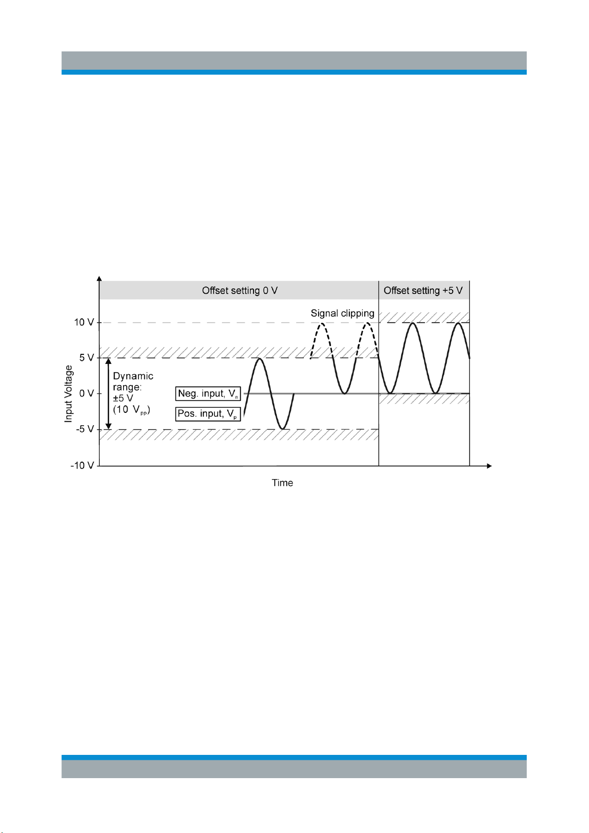
2.4 Offset Compensation
The R&S RT‑ZD10/20/30 features two offset compensation functions: a differential offset compensation and a common mode offset compensation. Each function
compensates a particular DC component of the input signal, even in front of the
active amplifier in the probe tip. For a definition of differential and common mode
input voltages, see Chapter 5, "Characteristics of Differential Probes",
on page 36.
18User Manual 1410.4550.02 ─ 05
Page 19
R&S®RT‑ZD10/20/30
2.4.1 Differential Offset
Putting into Operation
Offset Compensation
The dif
ferential offset compensation is often referred to as offset compensation.
The differential offset function can compensate a DC voltage applied between the
positive and the negative input socket. This is particularly helpful if a small singleended signal with a large DC offset is measured with a differential probe, for
example, with the negative input socket connected to ground. As the
R&S RT‑ZD10/20/30 measures differential voltages, setting a differential offset
compensation is directly visible on the oscilloscope screen as a voltage offset of
the measured waveform.
Figure 2-2: Differential offset compensation for a single-ended measurement (negative
input connected to ground) using an R&S
RT‑
ZD10/20/30
There are several ways to set the offset compensation:
●
Use the vertical knob at the oscilloscope if its function is set to of
●
Enter the offset value in the channel settings or probe settings on the
fset.
Rohde & Schwarz oscilloscope.
●
Use the micro button to measure input signals with different DC offsets: assign
"Offset to mean" to the micro button. See also Chapter 2.3.2, "Micro Button",
on page 18.
For more details, see the oscilloscope's user manual.
19User Manual 1410.4550.02 ─ 05
Page 20

R&S®RT‑ZD10/20/30
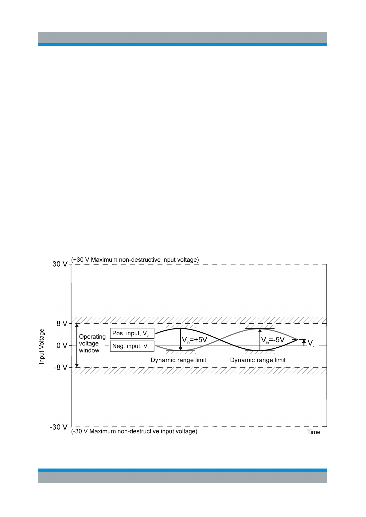
2.4.2 Common Mode Offset
Putting into Operation
Offset Compensation
Common mode of
serial number ≥ 200 000. It can compensate a common DC voltage applied to
both input sockets (referenced to the ground socket). This is particularly helpful
for measurements on differential signals with high common mode levels, for
example, current measurements using a shunt resistor.
fset compensation is available for R&S RT‑ZD probes with
Figure 2-3: Common mode (CM) offset compensation for a differential measurement
If the input signals fit into the operating voltage window of the
R&S R
tion.
T‑ZD10/20/30, it is not necessary to set a common mode offset compensa-
20User Manual 1410.4550.02 ─ 05
Page 21

R&S®RT‑ZD10/20/30
Putting into Operation
Offset Compensation
The R&S R
mode signals are suppressed by the probe. Therefore, the common mode
offset compensation is not directly visible on the oscilloscope screen, see
also Chapter 5.2, "Dynamic Range and Operating Voltage Window",
on page 38. An incorrect common mode offset compensation can lead to
unwanted clipping effects. Measuring the common mode input voltage
using the R&S ProbeMeter is a convenient way to detect breaches of the
operating voltage window.
If supported by the Rohde & Schwarz oscilloscope, you can set the
the probe settings on the instrument. For more details, see the oscilloscope's
user manual.
T‑ZD10/20/30 measures only differential input signals. Common
"CM offset" in
2.4.3 R&S ProbeMeter
The R&S ProbeMeter is an integrated voltmeter that measures DC voltages with
higher precision compared to the oscilloscope's DC accuracy
ment is performed continuously and in parallel to the time domain measurement
of the oscilloscope.
. The DC measure-
High-precision measurements are achieved through immediate digitization of the
measured DC voltage at the probe tip.
The R&S ProbeMeter measures the differential and common mode DC voltages
simultaneously and without reconnecting the probe. For a definition of differential
and common mode input voltages, see Chapter 5, "Characteristics of Differential
Probes", on page 36.
When the R&S ProbeMeter is active, the measured values are displayed on the
oscilloscope. The R&S ProbeMeter state is part of the probe settings of the channel to which the probe is connected. For details, refer to the user manual of the
Rohde & Schwarz oscilloscope.
Advantages of the R&S ProbeMeter:
●
Measures DC voltages of different levels, no need to adjust the measurement
range of the oscilloscope.
●
True DC measurement (integration time > 100 ms), not mathematical average
of displayed waveform.
21User Manual 1410.4550.02 ─ 05
Page 22

R&S®RT‑ZD10/20/30
Putting into Operation
Offset Compensation
●
High measurement accuracy and low temperature sensitivity
●
Simple means of setting the oscilloscope's trigger level and vertical scaling if a
waveform is not visible.
●
Independent of oscilloscope settings for offset, position, vertical scale, horizontal scale, and trigger.
●
Independent of probe settings for measurement mode and gain.
●
Unique way to detect unexpected or inadmissible common mode voltages,
e.g. bias points - measurement of common mode DC voltages without reconnecting the probe.
●
Differential measurement range ±5 V + offset compensation setting.
Common mode measurement range ±8 V + common mode offset compensation setting.
The R&S ProbeMeter enables the ground-referenced measurement of voltages.
A difference in the ground levels of oscilloscope and DUT can cause an unwanted zero error. In this case, correct the zero error, see Chapter 2.3.1, "Zero
Adjustment", on page 17.
.
22User Manual 1410.4550.02 ─ 05
Page 23
R&S®RT‑ZD10/20/30
R&S RT‑ZA15 External Attenuator
Key Characteristics
3 R&S R
The R&S R
ferential probe. It extends the input voltage range of the R&S RT‑ZD10/20/30
probe. Both dynamic range and operating voltage window are increased.
T‑ZA15 is an external 10:1 attenuator for the R&S RT‑ZD10/20/30 dif-
T‑ZA15 External Attenuator
3.1 Key Characteristics
The combination of R&S R
differential probe has the following key characteristics:
Attenuation 100:1
Bandwidth DC to 1.0 GHz (with R&S RT-ZD10)
Dynamic range (differential input) ±50 V with ±50 V offset capability
T‑ZA15 external attenuator and R&S RT‑ZD10/20/30
DC to 1.5 GHz (with R&S R
DC to 2.0 GHz (with R&S RT-ZD30)
T-ZD20)
Differential input resistance 1 MΩ
Differential input capacitance 1.3 pF
Observe maximum input voltage
T
o avoid electric shock and personal injury, observe the following limits:
●
The maximum input voltage for DC signals is ±60 V between each signal socket and the ground socket.
●
The maximum effective input voltage for AC signals is 30 V (eff)
between each signal socket and the ground socket. The maximum transient peak voltage is ±42.4 V.
●
The maximum input voltage is derated for higher frequencies. Refer to
the "R&S®RT-Zxx High Bandwidth Probes" data sheet for further information.
23User Manual 1410.4550.02 ─ 05
Page 24

R&S®RT‑ZD10/20/30
3.2 Description
R&S RT‑ZA15 External Attenuator
Inserting the Probe
The R&S R
T‑ZA15 external attenuator with inserted R&S RT‑ZD10/20/30 is
shown in Figure 3-1.
1 3 4 5 7
2
Figure 3-1: R&S
1 = Positive signal socket
2 = Negative signal socket
3 = Ground socket
4 = Trimmer for DC common mode rejection
5 = Trimmer for pulse response of positive input
6 = Trimmer for pulse response of negative input
7 = Notch for micro button
6
RT‑
ZA15 external attenuator with inserted R&S RT‑ZD10/20/30
The R&S R
T‑ZA15 external attenuator has the same tip - and the same signal
and ground sockets - as the R&S RT‑ZD10/20/30 probe head. All accessories for
the probe can be used with the external attenuator.
3.3 Inserting the Probe
To insert the probe in the R&S RT‑ZA15 external attenuator and enable it on the
oscilloscope proceed as follows.
1. Remove all accessories from the R&S RT‑ZD10/20/30 probe head.
2. Insert the probe into the rear opening of the attenuator with correct polarity.
Make sure that the "+" and "-" marks on the probe and the attenuator match,
and the notch for the micro button is on the same side as the micro button.
24User Manual 1410.4550.02 ─ 05
Page 25

R&S®RT‑ZD10/20/30
Attaching the attenuator with wrong polarity can damage the probe and the
external attenuator
3. Press the probe gently into the attenuator until the micro button matches the
notch on the attenuator in a central position.
.
R&S RT‑ZA15 External Attenuator
Adjusting
4. The oscilloscope does not detect the external attenuator automatically. To
adjust the scaling for display
tor in the probe setup of the oscilloscope. For more information, refer to the
user manual of your oscilloscope.
When you use the probe together with the external attenuator, hold them at
the gripping section of the external attenuator to ensure optimal mechanical
stability.
, R&S ProbeMeter and offsets, select the attenua-
3.4 Adjusting
The R&S R
measurements, further adjustment is not necessary. For use cases with specific
requirements to common mode rejection, it is possible to adjust the external
attenuator when you use it together with a specific R&S RT‑ZD10/20/30 probe.
Therefore, the external attenuator has 3 trimmers to adjust the common mode
rejection at DC and to adjust the pulse responses of the positive and negative
inputs.
T‑ZA15 external attenuator is already factory-adjusted. For usual
25User Manual 1410.4550.02 ─ 05
Page 26

R&S®RT‑ZD10/20/30
Adjusting the DC common mode rejection
R&S RT‑ZA15 External Attenuator
Adjusting
Equipment
Setup
●
R&S R
●
DC voltage source, max. output voltage 30 V, floating output, e.g.
HMP4040
●
BNC to 4 mm dual banana adapter
●
BNC to grabber adapter, e.g. Pomona mod. 3789
●
2 mini clips
●
2 leads, 6 cm/2.4 in
●
1 lead, 15 cm/5.9 in
●
Small skrewdriver
During the following procedure, both signal sockets (positive and negative) are connected to the Hi output of the DC voltage source. The ground
socket is connected to the Lo output of the DC voltage source.
●
Connect the probe to CH1 of the R&S R
●
Plug the BNC to 4 mm dual banana adapter onto the OUTPUT HI/LO
of the DC voltage source. Ensure that the BNC shield is connected to
LO.
●
Connect the BNC to grabber adapter to the BNC to 4 mm dual
banana adapter.
●
Using a mini clip and 2 leads, 6 cm/2.4 in, connect both signal inputs
of the external attenuator to the grabber. Use both inputs of the mini
clip.
●
Using a mini clip and a lead, 15 cm/5.9 in, connect the ground input of
the external attenuator to the shield of the BNC to 4 mm dual banana
adapter.
TO oscilloscope
TO oscilloscope.
26User Manual 1410.4550.02 ─ 05
Page 27

R&S®RT‑ZD10/20/30
R&S RT‑ZA15 External Attenuator
Adjusting
R&S RTO settings
Adjustment
●
Horizontal scale = 1 ms/div
●
Bandwidth = 20 MHz
●
V
ertical scale = 100 mV/div
●
Trigger source = Ch1, Trigger mode = Auto, Run cont
●
[Acquisition] key > Decimation Mode = High res, Waveform arithmetics = Average, Average Count = 10
●
"Meas" menu > Setup > Source = Ch1, Main Measurement = Mean,
State = On
●
"Vertical" menu > "Probe Setup" > "Ch" tab > "Attenuator RT-ZA15"
●
"Vertical" menu > Channels > Ch1 > Offset = 0 V, Position = 0 div
●
Set the voltage of the DC voltage source to 0 V.
●
Check the displayed value in the "Measurement Results" box: Mean =
V1.
●
Set the voltage of the DC voltage source to 30 V.
●
Check the displayed value in the "Measurement Results" box: Mean =
V2.
●
Using the small skrewdriver, turn the trimmer for DC common mode
rejection on the external attenuator until V2 = V1.
27User Manual 1410.4550.02 ─ 05
Page 28

R&S®RT‑ZD10/20/30
R&S RT‑ZA15 External Attenuator
Adjusting the pulse response of the positive and negative inputs
Adjusting
Equipment
Setup
●
R&S R
●
1 mini clip
1 lead 6 cm/2.4 in
Pulse response of the positive input:
●
Connect the probe to CH1 of the R&S R
●
"Vertical" menu > "Probe Setup" > "Ch" tab > "Attenuator RT-ZA15"
●
Using the lead and a mini clip, connect the negative input of the external attenuator to the ground clamp of the R&S RTO oscilloscope.
●
Press the positive input of the external attenuator directly to the
square wave signal clamp.
TO oscilloscope
TO oscilloscope.
R&S RTO settings
●
Horizontal scale = 1 µs/div
●
V
ertical scale = 200 mV/div
●
Trigger source = Ch1, Trigger mode = Auto, Run cont
●
Trigger level = 500 mV
Trigger slope = Positive
●
[Acquisition] key > Decimation Mode = High res, Waveform arithmetics = Average, Average Count = 10
28User Manual 1410.4550.02 ─ 05
Page 29

R&S®RT‑ZD10/20/30
R&S RT‑ZA15 External Attenuator
Adjusting
Adjustment
Setup and adjustment
●
Using the adjustment tool, turn the trimmer for pulse response of the
positive input on the external attenuator until an optimum square wave
response is visible on the oscilloscope screen.
Repeat the procedure to adjust the pulse response of the negative input:
●
Using the lead, connect the positive input of the external attenuator to
the ground clamp of the R&S R
●
Press the negative input directly to the square wave signal clamp.
●
Trigger level = -500 mV
Trigger slope = Negative
●
Using the adjustment tool, turn the trimmer for pulse response of the
negative input until an optimum square wave response is visible on
the oscilloscope screen.
TO oscilloscope.
Keep the adjustment of the positive and negative input as symmetric as
possible to ensure a good common mode rejection for AC signals.
29User Manual 1410.4550.02 ─ 05
Page 30

R&S®RT‑ZD10/20/30
Connecting the Probe to the DUT
4 Connecting the Probe to the DUT
This chapter describes the different ways of connecting the probe to the DUT. In
addition, the accessories supplied are described and their use is explained.
In order to achieve optimum RF performance, the connections should always be
as short as possible.
Risk of injuries
The included probe pins are exceptionally sharp and must be handled with
extreme care. T
removing pins.
o prevent injuries, always use tweezers when inserting or
Some solder-in accessories are very fine and sensitive. Stabilize the probe
using appropriate means (e.g. adhesive pads, probe positioner) in order to
protect the solder joint from excessive mechanical stress.
The R&S R
and ground sockets - as the R&S RT‑ZD10/20/30 probe head. All accessories for
the probe can be used with the external attenuator.
T‑ZA15 external attenuator has the same tip - and the same signal
30User Manual 1410.4550.02 ─ 05
Page 31

R&S®RT‑ZD10/20/30
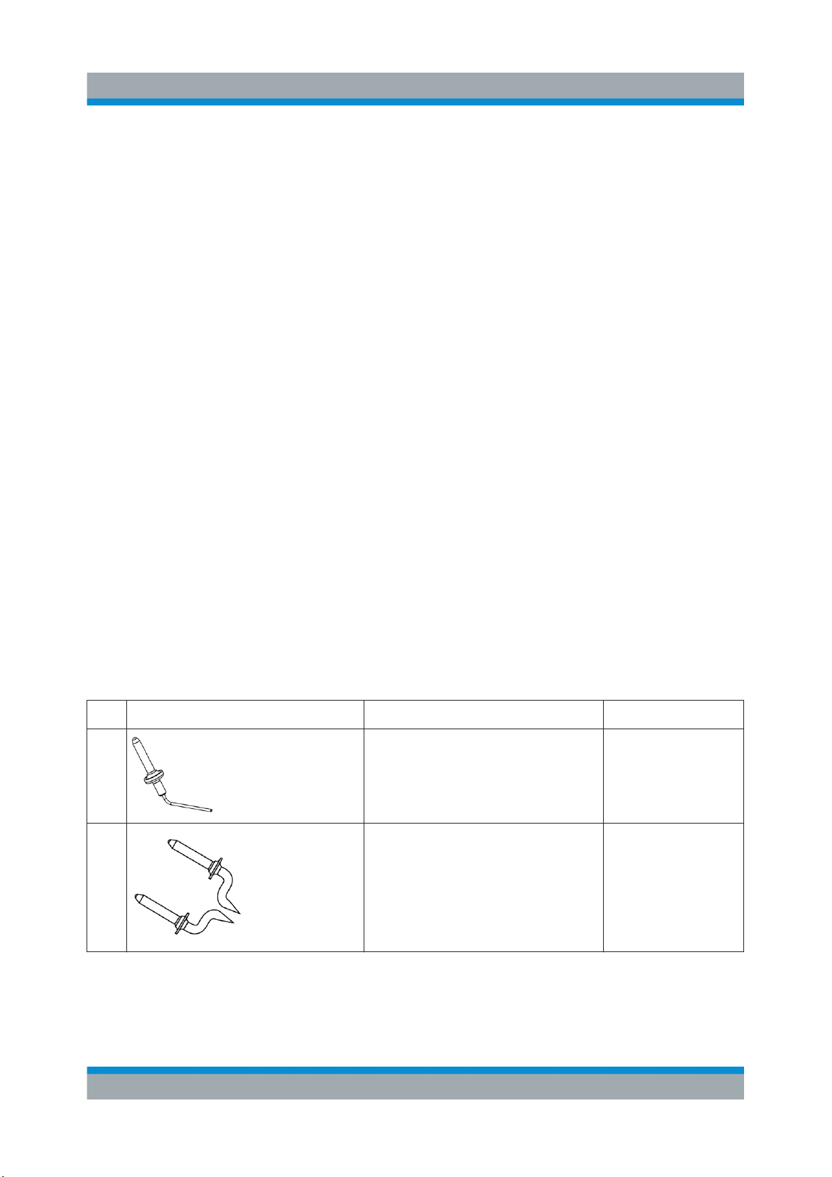
Pins
Signal pin, solder-in
Connecting the Probe to the DUT
Use tweezers to insert the solder-in pins into
the signal sockets on the probe, and then cut
to the appropriate length. T
as short as possible. Finally, stabilize the
probe, for example by using adhesive tape.
The fine wires on this adapter are best suited
to making secure contact with small contact
points, such as SMT components or IC pins.
The wires have an additional insulating finish
in order to prevent unwanted shorts. There is
no need to strip the wires because the finish
dissolves on its own during soldering.
Distance range: 0 mm to 25 mm (0 mil to
1000 mil)
ry to keep the wires
Signal pin, variable spacing
The signal pins are held to the DUT in order to
tap of
f the measurement signal. The pins can
be rotated to adjust the distance between the
probe tips. They are designed for various
applications, e.g. measurements on SMT
resistors, IC pins, conductors or vias.
Distance range: 0 mm to 10 mm (0 mil to 400
mil)
31User Manual 1410.4550.02 ─ 05
Page 32

R&S®RT‑ZD10/20/30
Adapters
Adapter, square pin
Connecting the Probe to the DUT
The square pin adapter is used for plugging
the probe onto pin strips with a pitch of 2.54
mm (100 mil).
Distance range: 2.54 mm (100 mil)
Browser adapter
The spring-loaded browser adapter allows
handheld probing with maximum convenience.
Because it compensates for minor unevenness and movements, it is capable of establishing a firm contact with the test point.
The pin distance can be set by turning the levers. A built-in stop prevents unwanted turning
of the signal pins when probing.
Distance range: 0 mm to 10 mm (0 mil to
400 mil)
32User Manual 1410.4550.02 ─ 05
Page 33

R&S®RT‑ZD10/20/30
Flex adapter, solder-in
Connecting the Probe to the DUT
The flex adapter is particularly well suited for
creating solid contact with test points that are
hard to reach (e.g. between two inserted
boards). The two wires at the tip of the flexible
line are soldered to the contact points. The
pins on the other end of the adapter are inserted in the signal receptacles of the probe.
The flex adapter reduces the probe rise time,
but is designed to ensure optimum settling.
The lines on the flex adapter are implemented
as a twisted pair to minimize unwanted coupling. Flex adapters are preferred over leads
or clips.
wo different flex adapters are included: 4 cm
T
(1.6 in) and 10 cm (3.9 in).
Distance range: 0 mm to 12 mm (0 mil to 470
mil)
Do not use the flex adapter at voltages beyond
±30 V.
Flex adapter, square pin
The flex adapter is used for plugging the probe
onto pin strips with a pitch of 2.54 mm (100
mil) that are hard to reach (e.g. between two
inserted boards). The pins on the other end of
the adapter are inserted in the signal receptacles of the probe. The flexible line makes it
possible to connect two or more probes to
adjacent pins without the probes blocking each
other
.
The flex adapter reduces the probe rise time,
but is designed to ensure optimum settling.
The conductors on the flex adapter are implemented as a twisted pair to minimize unwanted coupling. Flex adapters are preferred over
leads or clips.
Two different flex adapters are included: 4 cm
(1.6 in) and 10 cm (3.9 in).
Distance range: 2.54 mm (100 mil)
Do not use the flex adapter at voltages beyond
±30 V.
33User Manual 1410.4550.02 ─ 05
Page 34

R&S®RT‑ZD10/20/30
Connecting the Probe to the DUT
Leads and clips
Short and long lead
The lead provides a flexible connection to the DUT. It is plugged onto a pin on the DUT and can
be used to connect either the signal sockets or the ground socket. In addition, it allows micro
and mini clips to be connected to the probe.
Length:
Short lead: 60 mm (236 mil)
Long lead: 150 mm (591 mil)
Mini clip
The mini clip is designed for probing large IC
pins, wires and through-hole components.
For probing, clamp the mini clip to a pin and
connect it to the signal socket or the ground
socket using a lead.
34User Manual 1410.4550.02 ─ 05
Page 35

R&S®RT‑ZD10/20/30
Micro clip
Connecting the Probe to the DUT
The micro clip is designed for probing IC pins
and thin wires in fine-pitch applications.
The micro clip fits directly into the signal
socket or the ground socket using a lead.
35User Manual 1410.4550.02 ─ 05
Page 36

R&S®RT‑ZD10/20/30
2
np
cm
npin
VV
V
VVV
Characteristics of Differential Probes
5 Characteristics of Dif
A differential probe has three sockets: the positive signal socket (+), the negative
signal socket (-), and the ground socket.
Figure 5-1: Input voltages on a differential probe
Multiple input voltages can be defined for a differential probe:
ferential Probes
●
Dif
ferential mode input voltage (Vin, Vdm)
Voltage between the positive and negative signal sockets
●
Positive single-ended input voltage (Vp)
Voltage between the positive signal socket and the ground socket
●
Negative single-ended input voltage (Vn)
Voltage between the negative signal socket and the ground socket
●
Common mode input voltage (Vcm)
Mean voltage of positive and negative signal sockets referred to the ground
socket, respectively
Two of these voltages are independent values, the other two can be calculated:
Typically, the differential and the common mode input voltages are used to
describe the behavior of a dif
ferential probe.
36User Manual 1410.4550.02 ─ 05
Page 37

R&S®RT‑ZD10/20/30
cmvcminvdmout
VAVAV
vcm
vdm
A
A
CMRR
Characteristics of Differential Probes
Common Mode Rejection Ratio (CMRR)
The output voltage V
, which is displayed on the base unit, is obtained by super-
out
imposing the voltages generated from the differential mode input voltage and
from the common mode input voltage:
In this equation, A
A
is the amplification of the common mode input voltage.
vcm
An ideal differential probe is expressed as A
is the amplification of the dif
vdm
ferential mode input voltage and
= 1 and A
vdm
= 0. In this case, the
vcm
displayed voltage exactly equals to the differential input voltage Vin between the
two signal sockets, and the common mode input voltage is suppressed.
5.1 Common Mode Rejection Ratio (CMRR)
An ideal dif
input voltage Vin between positive and negative input, and suppresses the com-
ferential probe outputs a voltage that depends only on the differential
mon mode voltages. This is equivalent to an infinite common mode rejection ratio
(CMRR).
In contrast, real probes have a finite CMRR, resulting in a small part of the common mode voltage visible in the output signal. The CMRR is defined as the ratio
of the amplifications of differential and common mode input signals:
Example:
If a dif
ferential input voltage of 1 V yields an output voltage of 100 mV (A
and a common mode input voltage of 1 V an output voltage of 1 mV (A
vcm
vdm
=
= 0.1)
0.001), the CMRR is 100 (40 dB).
A high CMRR is important if significant common mode signals are encountered at
the probe input, for example:
●
DC voltages for setting the operating points of active DUTs
●
Different ground levels of probe and DUT, e.g. floating DUTs
●
An interference that couples equally to both conductors of a differential transmission line
37User Manual 1410.4550.02 ─ 05
Page 38
R&S®RT‑ZD10/20/30
Dynamic Range and Operating Voltage Window
●
Probing on ground-referenced signals. In this case, the common mode component is always equal to half of the input voltage.
Characteristics of Differential Probes
5.2 Dynamic Range and Operating V
Two separate specifications are necessary to characterize the permissible input
voltage range of a dif
●
The dynamic range (or "differential mode range") designates the maximum differential voltage Vin that may occur between the positive and negative signal
pin.
●
At the same time, the two voltage values at each of the two signal pins Vp and
Vn referenced to the common ground must not exceed a specific limit value.
This limitation is referred to as the operating voltage window (some manufac-
turers also use the less precise term "common mode range" for the same
parameter).
If one of these ranges is exceeded, an unwanted signal clipping may occur.
ferential voltage probe:
oltage Window
Figure 5-2: Operating voltage window
38User Manual 1410.4550.02 ─ 05
Page 39

R&S®RT‑ZD10/20/30
Signal clipping
Characteristics of Differential Probes
Ground Connection
Only dif
the base unit. Common mode signals are suppressed by the probe. Therefore, the user does not initially recognize that the operating voltage window
is exceeded owing to inadmissible common mode voltages. If unexpected
clipping occurs, check the positive or negative input voltage relative to
ground.
In addition, measuring the common mode input voltage using the R&S ProbeMeter is a convenient way to detect breaches of the operating voltage
window owing to excess DC common mode voltages.
ferential input signals are detected by the probe and displayed by
5.3 Ground Connection
It is typically not necessary to connect the ground socket of the probe to the
ground of the DUT
DUT is floating (such as in the case of battery operation), high static potentials
between the DUT ground and the probe ground can result in the operating voltage window of the probe being exceeded. In this case, the probe ground should
be connected to the DUT ground.
, as long as the DUT itself is grounded. If the ground of the
The ground connection can also affect the CMRR of the probe. Problems with
unwanted common mode signals can often be improved by adding a ground connection.
39User Manual 1410.4550.02 ─ 05
Page 40

R&S®RT‑ZD10/20/30
Measurement Principles
6 Measurement Principles
The R&S RT‑ZD10/20/30 differential probe provides an electrical connection
between the DUT and the oscilloscope. The probe transfers the voltage of the
electrical signal tapped off the DUT to the oscilloscope, where it is displayed
graphically. Although a probe has a wide variety of specifications, these specifications can be grouped into two classes of basic requirements:
●
High signal integrity of the transferred signal:
With an ideal probe, the output signal that is transferred to the base unit is
identical to the input signal between the probe tips, and signal integrity is
extremely high. Every real probe, however, transfers the input signal in altered
form. A good probe causes only minimum alterations.
How the probe can fulfill this requirement is mainly determined by its bandwidth and CMRR.
●
Low loading of the input signal:
Every probe is a load for the signal to be measured. The signal to be measured changes when the probe is connected. A good probe causes only a
minimum change to the signal, so that the function of the DUT is not adversely
affected.
How the probe can fulfill this requirement is mainly determined by its input
impedance.
The parameters of a probe are usually specified for a minimally short connection
between the probe and the DUT. With longer connections, the connection inductance has a significant effect on the measurement.
The high-frequency behavior of differential probes is typically characterized in the
following environment. The probe is connected to a differential 100 Ω line that is
fed by a source with 100 Ω internal impedance and that is terminated into 100 Ω.
The voltages at both inputs of the probe are always oppositely equal. The Fig-
ure 6-1 shows the equivalent circuit model of a probe that is connected to the
DUT.
40User Manual 1410.4550.02 ─ 05
Page 41

R&S®RT‑ZD10/20/30
Measurement Principles
Figure 6-1: Equivalent circuit model of the R&S
Table 6-1: Designations
Abbreviation Description
V
S
V
in
Differential voltage between the test point without probe connected
Differential voltage at the test point with probe connected, corresponds to the input voltage of the probe
R
S
R
L
R1, R
C1, C
L
con
2
2
Differential source resistance of the DUT
Differential load resistance of the DUT
Probe-specific input resistance
Probe-specific input capacitance
Parasitic inductance of the probe connection
RT‑
ZD10/20/30 probe
41User Manual 1410.4550.02 ─ 05
Page 42

R&S®RT‑ZD10/20/30
Measurement Principles
Signal Integrity of the Transferred Signal
6.1 Signal Integrity of the T
The following sections describe the effect that bandwidth, connection inductance
and common mode rejection ratio have on signal integrity
ransferred Signal
.
6.1.1 Bandwidth
The bandwidth BW of a probe is one of its specific parameters. The bandwidth of
the probe and the bandwidth of the base unit together form the system bandwidth. The following explanations refer to the probe itself, but can also be applied
to the entire system.
RT‑
Figure 6-2: Amplitude frequency response of the R&S
The bandwidth:
●
Specifies the maximum frequency at which a purely sinusoidal signal is still
transferred at 70 % (–3 dB) of its amplitude.
ZD10/20/30
42User Manual 1410.4550.02 ─ 05
Page 43

R&S®RT‑ZD10/20/30
BW
t
rise
4.0
Measurement Principles
Signal Integrity of the Transferred Signal
●
Specifies the transferable spectrum for other waveforms. E.g., with square
wave signals, the fifth harmonic should still be within the bandwidth for a high
signal integrity
●
Determines the minimum measurable signal rise time. The rise time t
.
probe is inversely proportional to its bandwidth. The following approximation
applies:
of the
rise
The Figure 6-3
shows a typical step response of an R&S RT‑ZD10/20/30 differen-
tial probe.
In addition to bandwidth, a constant amplitude frequency response of the probe is
decisive for high signal integrity. The Figure 6-2 shows the typical amplitude frequency response of an R&S RT‑ZD10/20/30 differential probe. All frequency components are transferred with the same gain so that the input signal is displayed
without distortion.
Figure 6-3: Step response of the R&S
RT‑
ZD10/20/30
43User Manual 1410.4550.02 ─ 05
Page 44

R&S®RT‑ZD10/20/30
con
incon
resonance
con
L
BW
CL
f
AL
1
toalproportion
2
1
≈
toalproportion
6.1.2 Connection Inductance
Measurement Principles
Signal Integrity of the Transferred Signal
The connection inductance L
is caused by connecting the probe to the DUT. In
con
contrast to the probe-specific bandwidth, the connection inductance mainly
depends on the selected type.
The connection inductance:
●
Increases with the length of the connection and the size of the resulting loop
area A.
See Figure 6-4.
●
Reduces the usable bandwidth and causes ringing with signals having a short
rise time, due to a series resonance with the input capacitance.
●
Must be as small as possible (short lead length) to maintain high signal integrity.
Figure 6-4: Ground connection and connection inductance using the example of R&S
ZD10/20/30
The T
as well as the associated connection inductance L
able 6-2 shows different types of connections between the probe and DUT
. The table also includes typ-
con
ical bandwidth values, rise time values, and the step responses for each connection in conjunction with an R&S RT-ZD30. For an R&S RT-ZD20, typical bandwidth and rise time values are smaller and limited to 1.5 GHz or 250 ps, respectively. For an R&S RT-ZD10, typical bandwidth and rise time values are also
smaller and limited to 1.0 GHz or 350 ps, respectively.
RT-
44User Manual 1410.4550.02 ─ 05
Page 45

R&S®RT‑ZD10/20/30
RT-ZD30 with different types
Measurement Principles
Signal Integrity of the Transferred Signal
Step response
-ZD30
Typ. bandwidth
and rise time
RT
, typical bandwidth, rise time and step response for a R&S
con
con
inductance
L
of connection
10 ps
1
~4 nH 3.2 GHz
120 ps
~8 nH 3.0 GHz
10 - 90%: 800 ps
~20 nH 700 MHz
very long settling
20 - 80%: 300 ps
time
~60 nH 500 MHz
Very short
signal pins, solder-in, variable
spacing
Short
browser adapters
Table 6-2: Connection inductance L
Type of connection Connection
adapters, square pin
Very long
Long
flex adapters (4.8 cm)
leads
micro clips
mini clips
45User Manual 1410.4550.02 ─ 05
Page 46

R&S®RT‑ZD10/20/30
Signal Loading of the Input Signal
Measurement Principles
6.1.3 CMRR
The CMRR is very good for low-frequency signals, but it continuously decreases
for higher frequencies. Therefore, the CMRR is usually specified as a function of
frequency.
The Figure 6-5 shows a typical CMRR for an R&S RT‑ZD10/20/30 differential
probe with a very symmetrical connection to the DUT. An asymmetrical connection to the test point can decrease the CMRR. To achieve the best possible
CMRR, the connection to the DUT should always be as symmetrical as possible.
Figure 6-5: Typical CMRR of the R&S
RT‑
ZD10/20/30 probe as a function of frequency
6.2 Signal Loading of the Input Signal
The previous section explained the transfer function and step response of the
probe. This section describes how the probe influences the input signal. The input
signal loading caused by the probe is determined by its input impedance. In general, the probe causes only low signal loading because its input impedance is
usually much greater than the source impedance of the test circuit.
46User Manual 1410.4550.02 ─ 05
Page 47

R&S®RT‑ZD10/20/30
Measurement Principles
Signal Loading of the Input Signal
6.2.1 Signal Loading for Differential Input Signals
The Figure 6-1 presents an equivalent circuit model of an R&S R
T‑ZD10/20/30
differential probe. The differential input impedance of the probe is equal to the
impedance between its positive (+) and the negative (-) signal socket. The resulting input impedance versus frequency is indicated in Figure 6-6.
Figure 6-6: Magnitude of the differential input impedance of the R&S RT‑ZD10/20/30 probe
as a function of frequency
The differential input impedance varies greatly versus the frequency and is
defined by the following values:
●
●
●
6.2.1.1 Input Resistance R
ferential input resistance Rdm = 2 R
Dif
1
Differential input capacitance Cdm = C1 + C2 / 2
Differential RF resistance RRF = 2 R
dm
2
The input resistance determines the loading of the DUT at DC and very low frequencies (< 100 kHz). A low input resistance can potentially disturb measurements of high-frequency signals as it influences the DC operating point of active
components.This effect is negligible for the majority of applications involving the
R&S RT‑ZD10/20/30 probe due to the very high input resistance of the probe
(1 MΩ).
47User Manual 1410.4550.02 ─ 05
Page 48

R&S®RT‑ZD10/20/30
Measurement Principles
Signal Loading of the Input Signal
6.2.1.2 Input Capacitance C
dm
The input capacitance Cdm causes the input impedance to decrease in the
medium-frequency range (100 kHz to 1.0 GHz). It affects the settling time of the
input voltage in the case of fast transients.
6.2.1.3 RF Resistance R
RF
The RF resistance RRF determines the minimum input impedance and thus the
maximum loading at very high frequencies above 1.0 GHz. Thus, the measure-
ment result depends on the source impedance of the DUT. The RF resistance R
prevents the input voltage from rising immediately to its final value in the case of
fast transients.
The resulting loading of a step signal at the input of the probe is shown in Fig-
ure 6-7.
RF
Figure 6-7: Signal loading caused by the R&S
RT‑
ZD10/20/30 probe
48User Manual 1410.4550.02 ─ 05
Page 49

R&S®RT‑ZD10/20/30
Measurement Principles
Probing Philosophy
6.2.2 Signal Loading for Non-Differential Input Signals
As described in Chapter 5, "Characteristics of Dif
various types of input signals can be measured with a differential probe. Every
type of input signal has an associated input impedance.
●
For differential input signals, the input impedance of the probe is the impedance between its positive and negative signal sockets.
●
For single-ended input signals, the input impedance is the impedance
between the positive or negative signal socket and the ground socket.
●
For common mode input signals, the input impedance is the impedance
between the parallel connection of the positive and negative signal sockets
and the ground socket.
The equivalent circuit diagram in Figure 6-1 can be used to determine the associated input impedance. The Table 6-3 provides as an example the DC input resist-
ance for several input signals.
Table 6-3: DC Input Resistance for Various Input Signals
Type of input signal Differential Single-ended Common mode
Input Resistance 1 MΩ 500 kΩ 250 kΩ
ferential Probes", on page 36,
This table shows that common mode signals suffer the highest loading. This characteristic of all dif
mode signals frequently have a very high source resistance (e.g. 10 kΩ for conventional fail-safe circuits). While the input resistance achieved for common mode
voltages with the R&S RT‑ZD10/20/30 differential probe remains sufficiently high,
probes with lower input resistances can lead to unfavorable loading effects.
ferential probes is particularly bothersome because common
6.3 Probing Philosophy
The previous sections explained that probes exert a load on the signal to be measured and change its characteristic. The signal at the test point where the probe
makes contact (Vin) is therefore different from the signal that was present before
the probe was connected (VS). This effect cannot be avoided and occurs with all
real probes – independent of type and manufacturer.
49User Manual 1410.4550.02 ─ 05
Page 50

R&S®RT‑ZD10/20/30
Measurement Principles
Probing Philosophy
As a result, there are different opinions which signal is the better output of the
probe:
●
The initial signal that is not loaded by the probe (VS), and that corresponds to
the signal at the test point without the probe being connected.
●
The input signal that is loaded with the input impedance of the probe (Vin) and
that is present between the probe tips.
Both approaches are physically correct and have their individual advantages and
disadvantages. In theory, it is even possible to convert mathematically the two
measurement results into each other, but conversion is a complex transformation
to and from the frequency domain. Probe manufacturers use one or the other of
these two approaches.
Rohde & Schwarz has decided in favor of the user-friendly approach. In our opinion, most users want to know the signal present in the DUT before it was altered
by the influence of the probe. Their goal is to characterize the DUTs, not the
probe.
If measurements are carried out in a 100 Ω (or a comparable) environment, the
signal displayed on the oscilloscope screen is always a direct representation of
the unloaded signal VS, see Figure 6-8.
Figure 6-8: Unloaded and loaded input signal and step response (for RT-ZS30)
50User Manual 1410.4550.02 ─ 05
Page 51

R&S®RT‑ZD10/20/30
Maintenance and Service
Contacting Customer Support
7 Maintenance and Service
Like all Rohde & Schwarz products, Rohde & Schwarz probes and adapters are
of high quality and require only minimum service and repair
or calibration is needed, contact your Rohde & Schwarz service center. Return a
defective product to the Rohde & Schwarz service center for diagnosis and
exchange.
7.1 Cleaning
1. Clean the outside of the product using a soft cloth moistened with either distilled water or isopropyl alcohol. Keep in mind that the casing is not waterproof.
. However, if service
Note: Do not use cleaning agents. Solvents (thinners, acetone), acids and
bases can damage the labeling or plastic parts.
Dry the product completely before using it.
2.
7.2 Contacting Customer Support
Technical support – where and when you need it
For quick, expert help with any Rohde & Schwarz equipment, contact one of our
Customer Support Centers. A team of highly qualified engineers provides telephone support and works with you to find a solution to your query on any aspect
of the operation, programming or applications of Rohde & Schwarz equipment.
Up-to-date information and upgrades
To keep your instrument up-to-date and to be informed about new application
notes related to your instrument, please send an e-mail to the Customer Support
Center stating your instrument and your wish. We will make sure that you get the
right information.
51User Manual 1410.4550.02 ─ 05
Page 52

R&S®RT‑ZD10/20/30
Europe, Africa, Middle East
Phone +49 89 4129 12345
customersupport@rohde-schwarz.com
North America
Phone 1-888-TEST-RSA (1-888-837-8772)
customer.support@rsa.rohde-schwarz.com
Latin America
Phone +1-410-910-7988
customersupport.la@rohde-schwarz.com
Asia/Pacific
Maintenance and Service
Returning for Servicing
Phone +65 65 13 04 88
customersupport.asia@rohde-schwarz.com
China
Phone +86-800-810-8228 / +86-400-650-5896
customersupport.china@rohde-schwarz.com
7.3 Returning for Servicing
Use the original packaging to return your R&S RT‑ZD10/20/30 to your
Rohde & Schwarz service center. A list of all service centers is available on:
www.services.rohde-schwarz.com
If you cannot use the original packaging, consider the following:
1. Use a sufficiently sized box.
2. Protect the product from damage and moisture (e.g. with bubble wrap).
3. Use some kind of protective material (e.g. crumpled newspaper) to stabilize
the product inside the box.
52User Manual 1410.4550.02 ─ 05
Page 53
R&S®RT‑ZD10/20/30
4. Seal the box with tape.
5. Address the package to your nearest Rohde & Schwarz service center.
Maintenance and Service
Spare Parts
7.4 Calibration Interval
The recommended calibration interval for R&S RT‑ZD10/20/30 differential probe
is two years. For servicing, send the probe to your nearest Rohde & Schwarz service center (see Chapter 7.3, "Returning for Servicing", on page 52).
7.5 Discarding the Product
Handle and dispose the product in accordance with local regulations.
7.6 Spare Parts
The following accessories can be ordered at the Rohde & Schwarz service center. Use the order numbers provided in the following table.
Table 7-1: Accessories spare parts
Pos Item Description Material Number
1
2 Signal pin, variable spacing 1417.0550.00
Signal pin, solder-in 1417.0538.00
53User Manual 1410.4550.02 ─ 05
Page 54

R&S®RT‑ZD10/20/30
Maintenance and Service
Spare Parts
Pos Item Description Material Number
3 Browser adapter 1417.0509.00
4 Adapter, square pin 1417.0573.00
5 Flex adapter, solder-in,
4 cm / 1.6 in
10 cm / 3.9 in
6
7 Lead, 6 cm / 2.4 in 1416.0128.00
8 Lead, 15 cm / 5.9 in 1416.0134.00
Flex adapter, square pin,
4 cm / 1.6 in
10 cm / 3.9 in
1417.0596.00
1417.0580.00
54User Manual 1410.4550.02 ─ 05
Page 55

R&S®RT‑ZD10/20/30
Maintenance and Service
Spare Parts
Pos Item Description Material Number
9 Mini clip 1416.0105.00
10 Micro clip 1416.0111.00
11 Marker band kit 1416.0205.00
12 External attenuator 1410.4744.02
13 Adjustment tool 1416.0057.00
14 Pogo pin Pogo pin connector, 6 pins 3584.6396.00
15 R&S RT-ZK2 R&S RT-ZK2 service kit 1410.5305.02
Table 7-2: Parts for ESD prevention
Pos. Item Material number
1 ESD wrist strap 0008.9959.00
2 ESD grounding cable 1043.4962.00
55User Manual 1410.4550.02 ─ 05
Page 56

R&S®RT‑ZD10/20/30
Functional Check
8 Functional Check
The functional check confirms the basic operation of the R&S RT‑ZD10/20/30 differential probe. The functional check is not suitable for verifying compliance with
the probe specifications.
1. Connect the R&S R
described in Chapter 2.1, "Connecting the Probe to the Oscilloscope",
on page 16.
2. Using a short lead and a mini clip, connect one of the signal sockets to the
square wave output
3.
Using a short lead and a mini clip, connect the other signal socket to the
probe ground connector
4.
Press the [Preset] key and then the [Autoset] key on the oscilloscope.
A square wave with 1 V amplitude between 0 V and 1 V is displayed on the
display.
5. Reverse the pins at the probe and repeat step 4.
T‑ZD10/20/30 to a Rohde & Schwarz oscilloscope as
of the oscilloscope.
of the oscilloscope.
56User Manual 1410.4550.02 ─ 05
Page 57

R&S®RT‑ZD10/20/30
Index
Index
A
Accessories
............................................. 10
AutoZero ..................................................17
B
Bandwidth ............................................6, 42
C
Cleaning .................................................. 51
Clipping ................................................... 39
Clips ........................................................ 13
CMRR ................................................37, 46
Common mode input voltage .................. 36
Common mode range ..............................38
Common mode rejection ratio ................. 46
Common Mode Rejection Ratio .............. 37
Connecting to DUT ..................................30
Connecting to oscilloscope ......................16
Connection inductance ............................44
D
Data memory .............................................7
DC measurement .................................... 21
Differential input voltage ....................36, 39
Dynamic range .................................... 6, 38
E
Electrostatic discharge ............................ 16
ESD ......................................................... 16
External attenuator .................................. 23
Adjusting ............................................. 25
Key characteristics ..............................23
Overview .............................................24
F
Functional check ..................................... 56
G
Ground connection .................................. 39
I
Inductance ...............................................44
Input capacitance ...................................... 6
Input resistance ......................................... 6
Input voltages .......................................... 36
L
Leads .......................................................13
Loading ....................................................46
M
Micro button .........................................6, 18
N
N/USB adapter ........................................ 13
O
Operating voltage window ....................... 38
P
Pins
Inserting and removing ....................... 30
Probe box .................................................. 9
Probe head ................................................8
Probe identification ..................................17
ProbeMeter ..........................................6, 21
Probing principles ....................................40
Product description ....................................5
S
Service kit ................................................14
Service manual ........................................14
Signal clipping ......................................... 38
Signal integrity .........................................42
Signal loading ..........................................46
Single-ended input voltage ......................36
Step response ......................................... 43
U
Unpacking ................................................. 7
Using accessories
Adapter ............................................... 32
Browser adapter ................................. 32
Ground adapter, square pin ................ 33
Ground pin, solderable, offset .............33
Leads .................................................. 34
Micro clip .............................................35
Mini clip ...............................................34
Signal pins .......................................... 31
Z
Zero error correction ................................17
57User Manual 1410.4550.02 ─ 05
Page 58

AlliCE
Messtechnik GmbH
make ALLICE your partner
ALLICE Messtechnik GmbH
Kelsterbacher Strasse 15-19 60528 Frankfurt am Main
Tel.: +49(0)69-67724-583 Fax: +49(0)69-67724-582
www.allice.de
© 2019 Allice Messtechnik GmbH – Alle Rechte vorbehalten.
© 2019 Allice Messtechnik GmbH – All rights reserved
Verwendete Warenzeichen und Schutzrechte sind Eigentum der jeweiligen Hersteller.
Logos and company names listed are trademarks or trade names of their respective owners.
info@allice.de
 Loading...