

Page 1

PDP TV Service Manual
Rolsen
Plasma display
television
Service Manual
Classis: MST9
Product Type: RP-42H10
Ver 1.0
1
Page 2

PDP TV Service Manual
Contents
Contents……………………………………………………........ -2-
Service Manual…………………………………………………. -2-
1. Product Safety Servicing Guidelines……………………. -3-
1-1 Safety precautions………………………………………-31-2 Product Safety notice…………………………………..-3-
2. Product Function Specifications…………………………..-4-
PDP4235EU product function…………………………...-4-
2-1
2-2
PDP4235EU specifications………………………………-4-
3. PDP panel spec……………………………………………...-7 3-1 General description……………………………………..-7 3-2 Panel block diagram……………………………………-8 3-3 Power (PSU) description……………………………… -8-
3-4 Power block diagram…………………………………...-9-
4. Block Diagram……………………………………………..-10 4-1 unite sketch map………………………………………-10 4-2 Video processing diagram…………………………...-13 4-3 Audio processing diagram…………………………..-14-
5. Service Mode and Adjustment………………………….. .-14 5-1 Service mode…………………………………………...-14-
6. Software updating…………………………………………..-18 6-1
7.
PDP4235EU Explode View and Bom………………………-29-
PDP4235EU software updating……………………….-18-
7-1 Spare Parts List………………………………………..-29-
9. Troubleshooting…………………………………………….-30-
10. Stand installing…………………………………………… -32-
11.
PDP Wall-mounting Bracket Installation Guide…………..-33-
12. Circuit Diagram…………………………………………….-36-
Hisense confidential
2
Page 3

PDP TV Service Manual
Product Safety Servicing Guidelines
CAUTION: BEFORE SERVICING THE CHASSIS, READ THE “SAFETY
1. Safety precautions
WARNING:
Service should not be attempted by anyone unfamiliar with the necessary precaution on this
receiver. The following are the necessary precautions to be observed before servicing this
chassis.
1. When replacing a chassis in the cabinet, always be certain that all the protective devices are put
back in place, such as: non-metallic control knobs, insulating covers, shields, isolation
resistor-capacitor network etc.
2. When replacing parts or circuit boards, disconnect the power cord.
3. When replacing a high wattage resistor (oxide metal film resistor) on the circuit board, keep the
resistor 10mm (1/2in) away from circuit board.
4. Connection wires must be kept away from components with high voltage or high temperature.
5. If any fuse in this TV receiver is blown, replace it with the FUSE specified in the chassis parts
list.
PRECAUTION” “PRODUCT SAFETY NOTICE”ON PAGE 3 OF
THIS MANUAL.
2.Product Safety notice
Many electrical and mechanical parts in the chassis have special safety-related characteristics.
These characteristics are often passed unnoticed by a visual inspection.
Replacement parts, which have these special safety characteristic are identified in this manual
and its supplement electrical components having such features are shaded on the schematic
diagram and the parts list.
Before replacing any of these components, read the parts list in this manual carefully. The use of
substitute replacement parts, which do not have the same characteristic as specified in the parts
list may create shock, fire or other hazards.
NOTES:
Screen Image retention Do not display a still image (such as on a video game or when
hooking up a PC to this PDP) on plasma monitor panel for a long time as it can cause screen
image retention. This image retention is also known as “screen burn”. To avoid such image
retention, reduce the degree of brightness and contrast of the screen when displaying a still
image.
A still image displayed too long may cause permanent damage to the PDP Panel
Watching the PDP TV in 4:3 format or other non full screen formats for a long period of time may
leave traces of borders displayed on the left, right and centre of the screen caused by the
difference of light emission on the screen. Playing a DVD or a game console may cause similar
effect to the screen. Damages caused by the above effect are not covered by the Warranty.
Afterimage on the Screen Displaying still images from Video games and PC for longer than a
certain period of time may produce partial afterimages. To prevent this effect, reduce the
brightness and contrast when displaying still images for a long time.
Height The PDP can normally operate only under 2000m in height. It might abnormally function
at a place over 2000m in height and do not install and operate there.
℃
Avoid operating the TV at temperatures below 5
Warranty Warranty does not cover any damage caused by image retention; Burn-in is not covered
by the warranty.
(41°F)
Hisense confidential
3
Page 4

PDP TV Service Manual
Product Fuction Specifications
1.PDP4235EU product function
·High end flat display
·HDMI input
·High definition compatible
·Wide Screen display optimized for cinema viewing
·Multimedia display :TV/PC
·High clear picture
·Audio equalizer
·Color enhancer ,contrast enhancer
·Two Scarts ,Scart1 (RGB/CVBS),Scart2(CVBS)
2. PDP4235EU specifications
Hisense confidential
4
Page 5
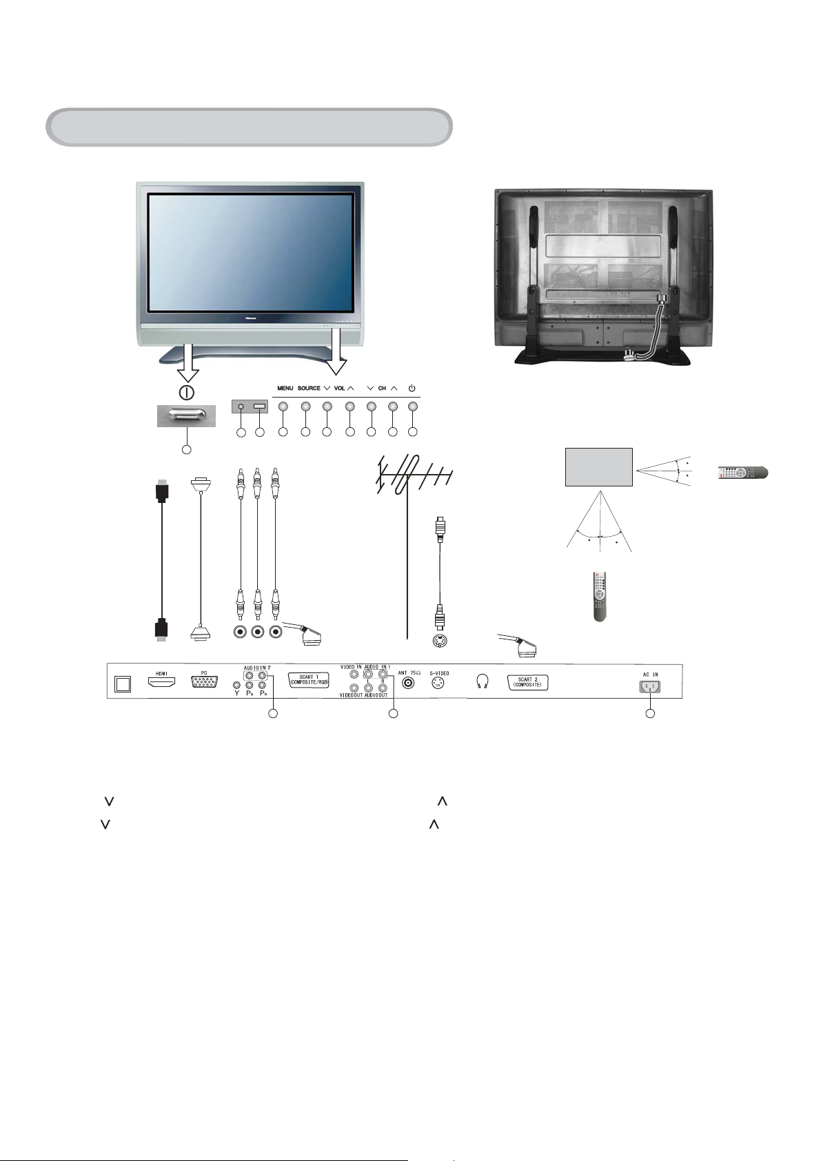
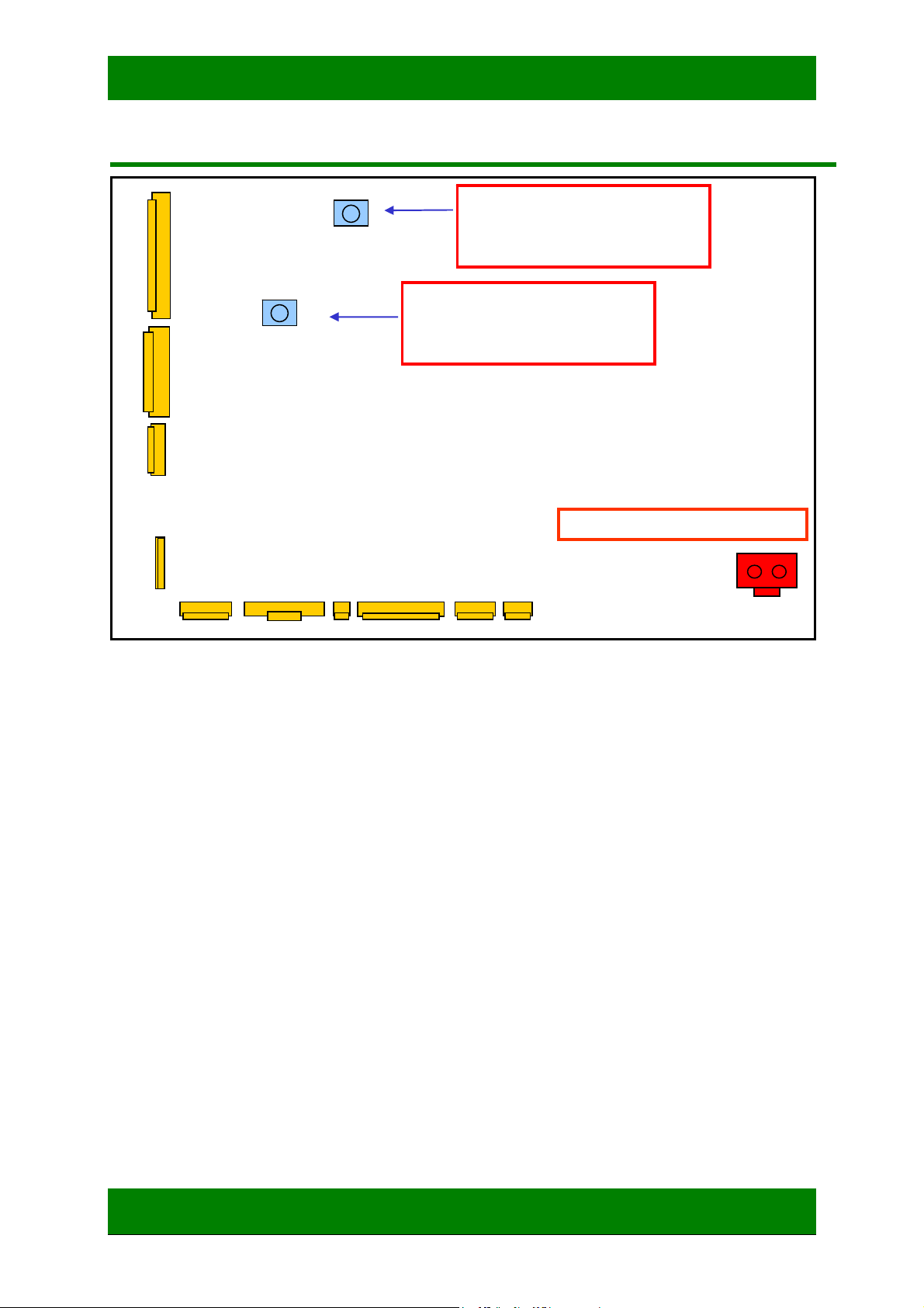
Viewing the Connection Panel
POWER
Power Cord
5
10
1
8
7
2
43
6
IR angle for the remote control
11
screen
6m
30
30
6m
8m
Source
1
TV
Zoom
Sound
Picture
3
2
1
5
6
4
9
8
7
Display
Recall
0
CH
VOL VOL
1
CH
I/ii
u
n
e
M
Still
Mute
IndexHold
Hold
Text
Sleep
Move
Pip
Cancel
Mix
Reveal
Subcode
Swap
ce
Sour
1
Give Name
Y
P
B
PR
DIGITAL
AUDIO OUT
13 12
1 Menu button : activate OSD menu 2 Source button : activate OSD source select
3 VOL : 4 VOL :
5CH: 6CH:
Volume decrease / Left button Volume increase / Right button
Previous channel / Down button Next channel / Up button
7 POWER indicator 8 Remote sensing window
9 AC Power socket 10 Power switch(standby)
11 Power switch(on/off) 12 VIDEO/S-VIDEO Audio input
13 PC/YP P Audio input
BR
6m
15
8m
15
6m
I/ii
Text
CancelSubcode
TV
Source
Mix
Still
9
6
3
Sleep
isplay
Zoom
D
p
CH
CH
0
8
5
Reveal
2
Swa
Index Hold
Move
Mute
Sound
ce
u
n
ur
e
VOL VOL
Pip
Hold
call
7
4
1
M
So
Picture
Re
1
1
1
9
Note: The above figures are for reference only, please refer to the actual units to determine the appearances.
Page 6
PDP TV Service Manual
PDP4235EU
PDP panel Plasma panel 42''
Native Screen Resolution 852 x 480
Television system SECAM/PAL
Sound system BG / DK / I
Channel coverage VHF-L: E2-S8
VHF-H: S9-S37
UHF: S38-E69
PC mode (DB15) 60Hz
640 x 480, 800 x 600, 1024 x 768
YPBPR mode 50Hz
576 i/p, 720p, 1080i
60Hz
480i /P,720p, 1080i
HDMI mode RGB 640 x 480, 800 x 600, 1024 x 768
YPBPR 50Hz
576p, 720p, 1080i
YPBPR 60Hz
480p; 720p, 1080i
Static contrast ratio 40 : 1
Brightness 400 cd/m²
Viewing angle 140° (H/V)
Power source
Power consumption 300W
Audio output 2 x 7 watts
Audio filter Equalizer 5 x bands
Connection interface
Dimensions 1054mmX812mmX331mm (LXWXH)
AC 100V-240V,50/60Hz
RF Input: RF Antenna x 1
Video Input: YUV x 1 ,S-Video x 1,AV x 1
Graphic
Input:
Audio Input: YUV x 1 ,S-Video /AV x 1,PC analog
Audio
Output:
Video
Output:
Other:
(including stand)
PC analog (DB15) x 1,HDMI x 1
(HDCP)
(DB15) x 1
audio output x 1
headphone x 1 (Jack 3,5mm)
video output x 1
Hisense confidential
6
Page 7
PDP TV Service Manual
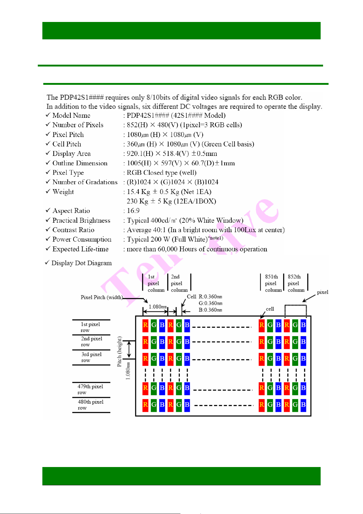
PDP panel spec
1. General description
Hisense confidential
7
Page 8
PDP TV Service Manual
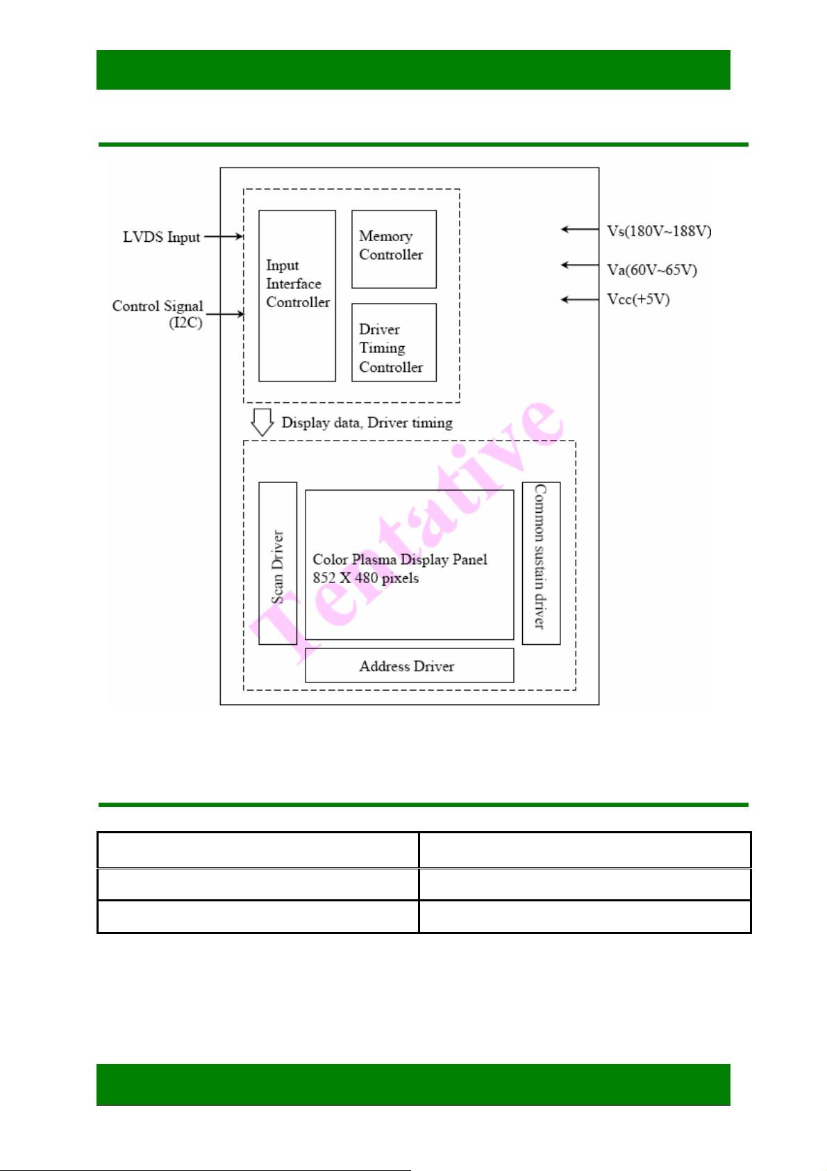
2. Panel block diagram
3.Power (PSU) description
Standard Voltage Range
A vail able Voltage Range
Frequency Range
AC 100V ∼ 240V
AC 90V ∼ 265V
50Hz ∼ 60Hz(± 5Hz)
Hisense confidential
8
Page 9
PDP TV Service Manual
Shipment Condition : 185
Shipment Condition : 60V
4.Power block diagram
VS
CN806
VR901
* Vs Voltage Variabe Resistor
- Turn right, increase Voltage
Turn left, decrease Voltage
•
V
VA
CN807
CN805
CN701
VR951
CN809 CN801 CN804
* Va Voltage Variable Resistor
- Turn right, increase Voltage
Turn left, decrease Voltage
•
CN803
CN810
CN802
* Connect with Noise Filter
Neutral
Live
CN1
Hisense confidential
9
Page 10
PDP TV Service Manual
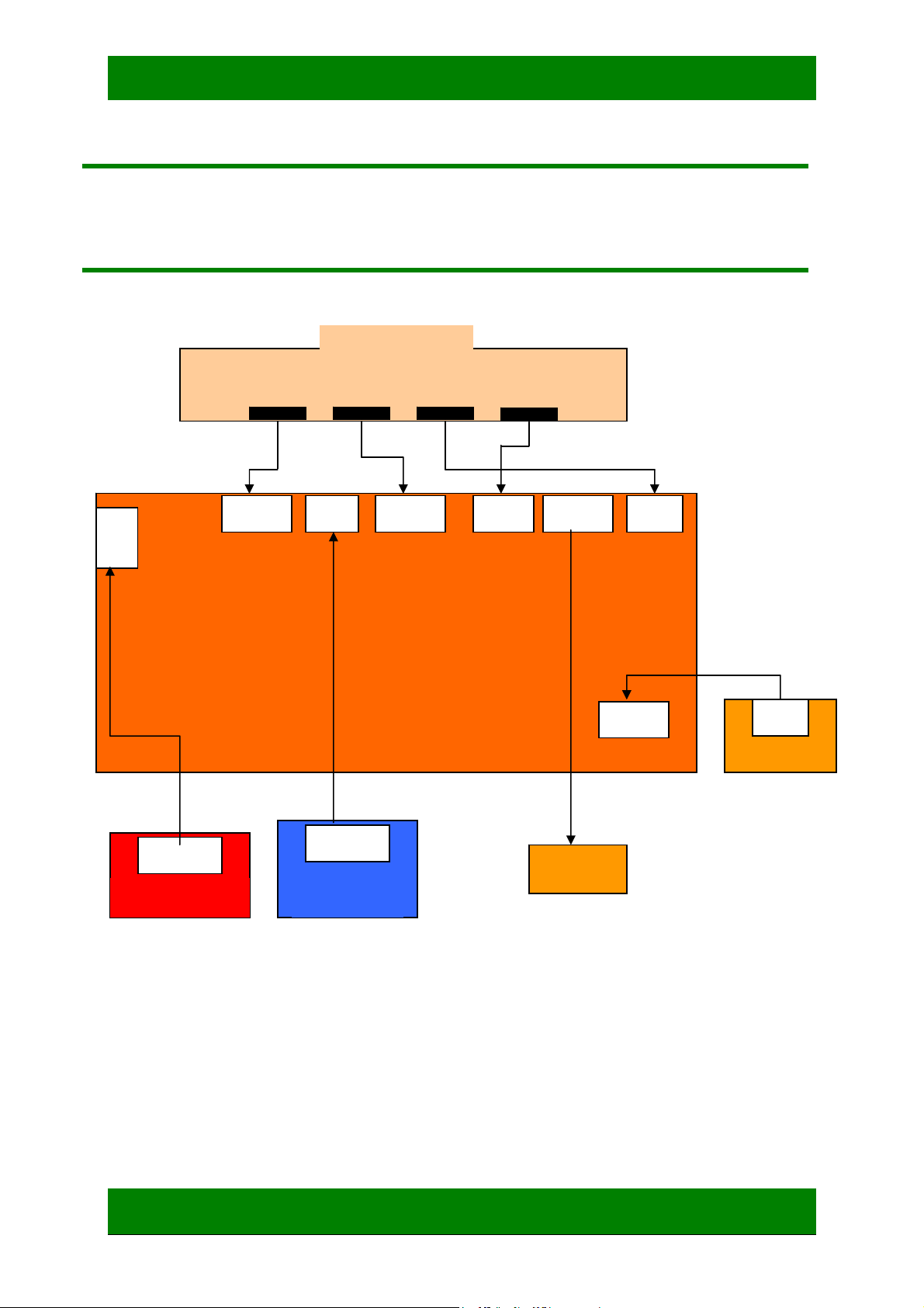
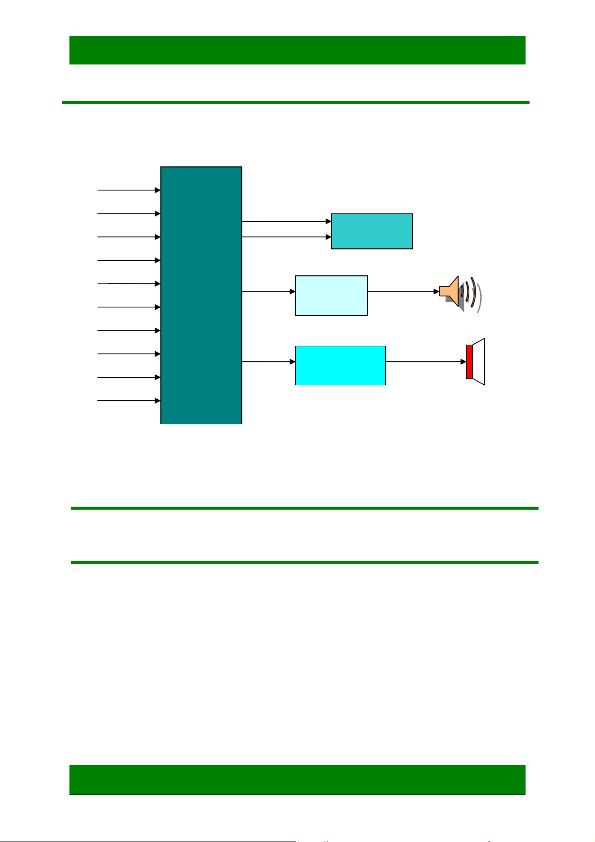
Block Diagram
The signal board is composed by the main board .The main chip for video decoder is
MST9E88L produced by MSTAR co., ltd.
1. unite sketch map
CN801 CN804 CN803 CN802
POWER SUPPLY
J20
XPR01
REMOTE BOARD.
MAIN BOARD
XPK01
KEY BOARD
970A
XP25 XP26XP24 XP3
961A
XP10 XP7
XP31
SPEAKER
XP1
SCART BOARD
Hisense confidential
10
Page 11
PDP TV Service Manual
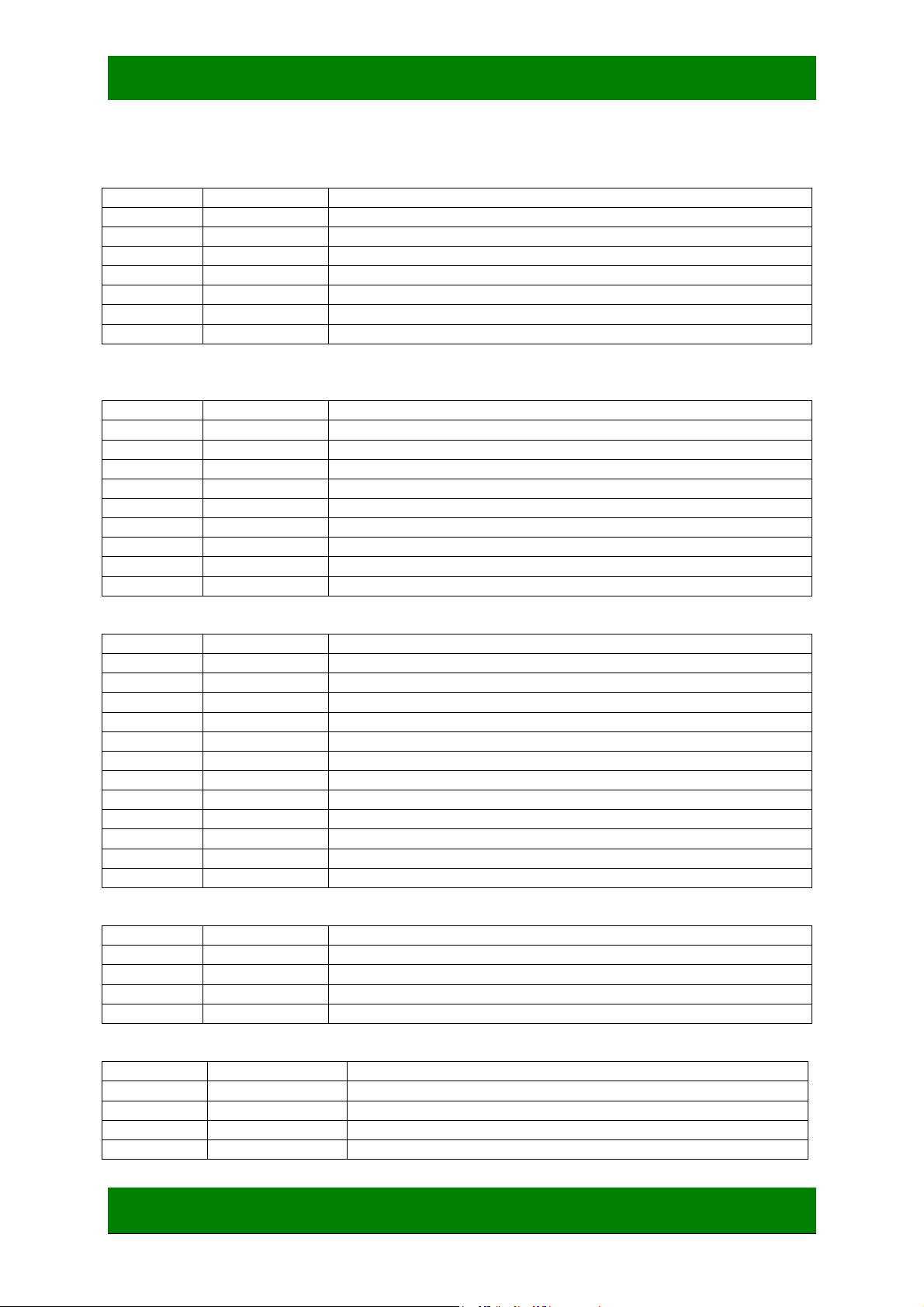
FUNCTION OF CONJUNCTIONS
CN801---XP24
ITEM NAME FUNCTION
1 ACD GND
2 RLY_ON HIGH LEVEL (ON)
3 5VSTB 5V POWER
4 GND GND
5 VSON HIGH LEVEL (ON)
6 5VD NO USED
7 NC NO USED
CN804---XP25
ITEM NAME FUNCTION
1 9VSC power for tuner
2 9VSC power for tuner
3 GND GND
4 5VSC +5V POWER
5 5VSC +5V POWER
6 5VSC +5V POWER
7 GND GND
8 GND GND
9 GND GND
CN803--- XP7
ITEM NAME FUNCTION
1 5VSC +5V POWER
2 5VSC +5V POWER
3 5VSC +5V POWER
4 GND GND
5 GND GND
6 GND GND
7 12VSC power for amplifier LM833
8 12VSC power for amplifier LM833
9 GND GND
10 GND GND
11 12VF NO USED
12 GNDF GND
CN802---XP26
ITEM NAME FUNCTION
1 30V power for amplifier TDA8932
2 30V power for amplifier TDA8932
3 GND GND
4 GND GND
XPK01---XP3
ITEM NAME FUNCTION
1 +3.3V NO USED
2 KEY0 KEY CONTROL
3 KEY1 KEY CONTROL
4 GND GND
Hisense confidential
11
Page 12

PDP TV Service Manual
XPR01---XP4
ITEM NAME FUNCTION
1 IR REMOTE CONTROL
2 GND GND
3 LEDR LED CONTROL
4 GND GND
5 5VST_B POWER OF REMOTE
6 GND GND
XP1---XP31
ITEM NAME FUNCTION
1 AV1 SCART2 _Y SIGNAL
2 GND GND
3 A-C SCART2_C SIGNAL
4 S-PI8 SCART2 FUNCTION SELECT
5 A-L SCART2 AUDIO IN_L
6 A-R SCART2 AUDIO IN_R
7 A-OUT VIDEO OUTPUT
8 GND GND
9 S-LOUT AUDIO OUTPUT_L
10 S-ROUT AUDIO OUTPUT_R
Hisense confidential
12
Page 13
PDP TV Service Manual
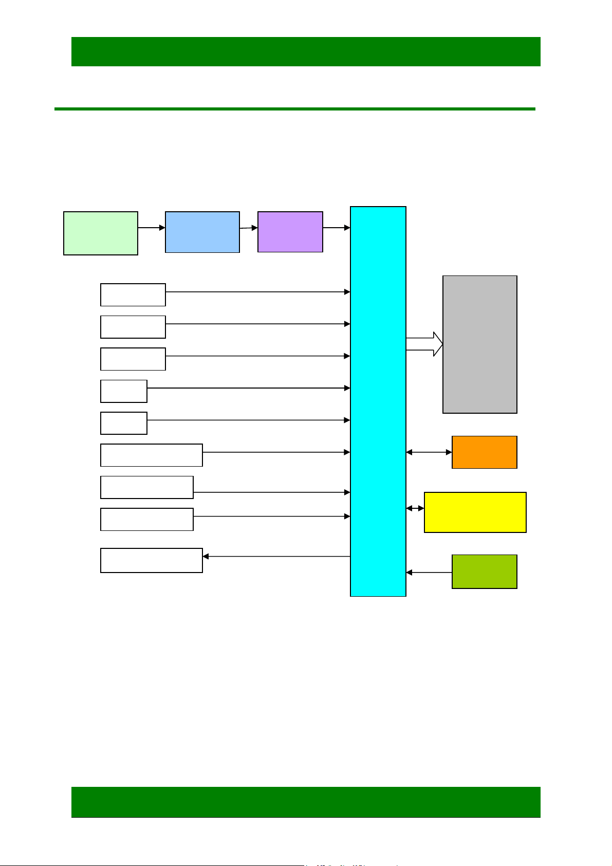
2. Video processing diagram
TUNER
TDQ-6FT/W
116H
YPBPR
VIDEO
S-VIDEO
HDMI
PC
SCART1 _CVBS
SCART1_ RGB
SCART2 _CVBS
VIDEO OUTPUT
SAW FILTER
HS9455
HS6274
IF
TDA9886
CPU
MST
9E88L
PDP module
PDP42S1
FLASH
PS25V040
SDRAM
HY5DU281622F
KEY/
REMOTE
Hisense confidential
13
Page 14
PDP TV Service Manual
3. Audio processing diagram
VIDEO -L
VIDEO-R
TV-SIF
YPBPR/PC-L
YPBPR/PC-R
HDMI-IIS
SCART1-L
SCART1-R
SCART2-L
SCART2-R
MST9E88L
CPU
AV-L
AV-R
AUDIO OUT
Amplifier
LM833
Amplifier
TDA8932T
Earphone
Speaker
Service Mode And Adjustment
1.Service mode
You can entry service mode menu by follow steps:
1. Press on the [MENU] key.
2. Select the sub-menu [SOUND] with [CH∧/CH∨].
3. Select the parameter [BALANCE] with the keys [VOL∧/VOL∨].
4. Press a series of numbers [0] [5] [3] [2] quickly.
SERVICE MODE MENU includes:
Fac. Menu
Hisense confidential
14
Page 15

PDP TV Service Manual
Factory Menu
White Balance
Auto Calibration
LOGO
OSD Language
Country
Option
Factory Init
Test Pattern
Version:
Auto Calibration
Auto Color
Color Temp. Standard
RED COLOR 126
GREEN COLOR 128
BLUE COLOR 135
White Balance
R DRV 10
G DRV 9
B DRV 12
R CUT 126
G CUT 128
B CUT 135
BRIGHT_H 80
CONTRAST _H 80
BRIGHT_L 40
CONTRAST_L 40
LOGO
NULL
HISENSE
WELCOME
Hisense confidential
15
Page 16

PDP TV Service Manual
Option
SOURCE TV
BRIGHT 0 10
BRIGHT 50 100
BRIGHT 100 145
CONTRAST 0 60
CONTRAST 50 120
CONTRAST 100 155
TOFAC M
HDMI Cable Standard
PIXSHIFTNUMBER 1
PIXSHIFTTIME 30
Test Pattern
BLUE
Factory Init
QingDao
HuangDao
Guiyang
Hungary
France
Austria
CLEAR PROTECTLY
CLEAR UNPROTECTLY
Version
Version:
PDP4235EU_VER1.40.20070620
Panel Type:
LG 42S1 (852*480)
FLASH :
PS25LV040
Hisense confidential
16
Page 17

PDP TV Service Manual
Design Menu
Picture Mode
Sound Mode
Sound Settings
Power Save
PIP Option
EMI
MOVESHARPNESS
LipSync
Picture Mode
Standard Brightness 50
Contrast 50
Colour 50
Bright Brightness 60
Contrast 55
Colour 55
Soft Brightness 45
Contrast 45
Colour 45
Sound Settings
VOLUME 0 120
VOLUME 1 60
VOLUME 20 40
VOLUME 40 25
VOLUME 100 11
TVPRE SCALER 5
VOLUME SCALER 0
Sound Mode
Standard 120Hz 12
500Hz 10
1.5KHz 11
5KHz 8
10KHz 15
Music 120Hz 19
500Hz 11
1.5KHz 12
5KHz 14
10KHz 20
Speech 120Hz 4
500Hz 10
1.5KHz 12
5KHz 7
10KHz 5
Hisense confidential
17
Page 18

PDP TV Service Manual
NOTE: We advise service hadn’t better amend factory data, because it is better settings data.
Please do not tell user the purpose password.
Software updating
PDP4235EU software updating
1、You can update the software through a special tool (show as below)
2、Software Updating Operation
1.Connect the Debug board to the TV use VGA interface, then connect the Debug board to the
computer, just as the pictures showing.
Hisense confidential
18
Page 19

PDP TV Service Manual
2.Set the ISP_TOOL4.0.9 -------only for the first time update.
DLPORTIO.dll and FTD2XX.DLL must be in the same folder
1)Find the folder where the ISP_TOOL4.0.9 lies in.
Hisense confidential
19
Page 20

PDP TV Service Manual
Note: DLPORTIO.dll and FTD2XX.DLL must be in the same folder.
2)Double click the ISP_TOOL4.0.9 icon, and then a dialog will show as below.
3)Click the Config button. And then a dialog will show as below.
You should set the Config like what the picture shows.
Hisense confidential
20
Page 21

PDP TV Service Manual
Hisense confidential
21
Page 22

PDP TV Service Manual
Hisense confidential
22
Page 23

PDP TV Service Manual
4) After you have finished all above, you should click the Apply button to complete the
configuration.
3. Turn on the TV, then we can update.
4. Double click the ISP_TOOL4.0.9 icon, and then a dialog will show as below.
5. Click the Read button. And then do as shown below.
Hisense confidential
23
Page 24

PDP TV Service Manual
6. Find the update file in your computer.
Hisense confidential
24
Page 25

PDP TV Service Manual
7. Double click the update file. A dialog will show as below.
Hisense confidential
25
Page 26

PDP TV Service Manual
8. Click the Auto button. And then do as shown below.
Hisense confidential
26
Page 27

PDP TV Service Manual
9. Click the Connect button. And then do as shown below.
Hisense confidential
27
Page 28

PDP TV Service Manual
10. Click the Run button.
11. When the update is finished, a dialog will show as below.
Hisense confidential
28
Page 29

PDP TV Service Manual
PDP4235EU Explode View and Bom
Spare Parts List
Main Spare Parts
Name
1
2
3
4
5
6
7
8
9
10
11
Type
Part No.
Hisense confidential
29
Page 30

PDP TV Service Manual
N
N
m
Troubleshooting
1.
o picture
2.
Abnormal display
3.
Enlarged display
P.LED
OFF
blue
OSD?
Check power connections
ok
o proble
OSD ?
no
L.Led?
flickering
red
Press [zoom]on the remote control to check whether it is
in zoom mode
The TV system has wrongly identified 625-lines system as
525-lines system. Change to another source (such as video,
pc) and change back to TV to correct it
Press [power] on the remote to quit stand-by mode
ok
no
Check main board connections or
change main board
Check LVDS connection or module
connections
off
Check LVDS
connection
Check module
driver Board
connections
Hisense confidential
30
Page 31

PDP TV Service Manual
N
m
r
gram
N
4.
o sound
Check audio board connections o
change audio board
5.
Black bars on panel
Red (green/blue) line on panel
Red (green/blue) stripe on panel
Big noise from panel
Note:
p.LED?
Power indicator at the centre of the front panel. Normal state : blue; remote command state: blue flickering.
L.LED?
LVDS indicator on the logic processing board. Normal state: yellow flickering.
OSD?
Press [MENU] to display menu on the screen.
TV audio?
no
Check TV channel input part circuit diagram
ok
no
Check TV channel input part circuit
dia
ok
Press mute button
no
ok
Replace the plasma display
module with spare parts
o proble
Check other
channel?
Hisense confidential
31
Page 32

PDP TV Service Manual
Problem solutions:
1. Adjusting sharpness can improve picture definition.
2. Adjusting bright can improve picture administrative levels, it can display black background something.
3. If VGA or YPBPR color isn’t natural. You can optimize VGA.
4. PDP power is very large system. As you power off power. Power component must discharge period of
time. Power can work steadily. If you power off and power on TV continuously. Then power work
unsteadily. Then PDP TV will display deviant picture.
5. TV, AV and S.video are the same white balance setting. VGA is a set white balance setting. HDTV is a
set white balance setting.
6. Picture mode does be divided four modes. such as standard, brightness, soft and custom. If you adjust
factory data, they will increase the same data.
7. If TV don’t work normally, it will take place follow some phenomena.
No. Trouble Measure
1 Turn on the TV, The LED is red, no display
on screen
2 Turn on the TV, The LED is blue, but no
picture or/and no sound
3 In TV state, can not to tuning You should to replace the main board.
4 No teletext You should to replace the main board.
5 No sound You should to replace the main board.
6 can not to updating software You should to replace the main board
7 No reaction with PC You should change the main board
8. If the picture color is not correct in the scart1 RGB source, but the scart1 CVBS is normal .you can
check the fast blank signal is whether high. If it is low, please check the circuit.
9.If the picture is not normal 16:9 mode or 4:3 mode when the signal equipment send 16:9 mode or 4:3
mode, please check the aspect mode whether is in “normal” mode.
Replace the main board or updating the
software.
You should to replace the main board.
Stand installing
Assemble instruction
Mount Installation
Mount Preparation
1. Take the mounting components out of the box.
2. Fix stanchion A and stanchion B onto the base subassembly with two screws (M6x20) as
Fig.1, turn the screws to tighten it.
3. Assemble the base subassembly onto the TV set with screw (M8X15) and screw (M5X12)
as Fig.2.You can find these screws in the box of the base.
NOTE: Failure to do so may result in breaking, denting and scratching the plasma display.
Hisense confidential
32
Page 33

PDP TV Service Manual
PDP Wall-mounting Bracket Installation Guide
READ CAREFULLY BEFORE INSTALLATION!
THE INSTALLATION GUIDE SHOULD BE RETAINED FOR FUTURE REFERENCE.
Caution:
Hisense confidential
33
Page 34

PDP TV Service Manual
1. Do NOT attempt to install the TV by yourself to avoid mistakes or hazard. Refer all installation to
qualified servicing personnel.
2. Do NOT install the TV on a wall aslope or a wall that makes the TV screen sloping over 25°off plumb
line. Otherwise, it may cause tumble or injury.
3. Refer all installation to qualified servicing personnel.
4. One must follow the instructions in this guide to correctly install the TV.
5. It requires more than one person to install the TV.
6. Before installation, examine whether the wall conforms to the specifications and whether the supplied
parts can be fixed on it. The wall for mounting should sustain the weight of TV and speakers, e.g.
cement wall or brick wall. Do NOT attempt to install the TV on a flexible wall such as sand wall or
plaster wall, unless the bolt are fixed on an area with standard building rigidity which sustains the
weight of the TV and speakers. If the rigidity of the wall can not be measured, every mounting hole
should sustain a frontal force of over 100N and a shearing force of over 200N.
7. Use the specified electric drill and drill bit for drilling. The drilling holes should conform to the
specifications.
8. To avoid fire and shock, do NOT place radiator, heater or humidifier below the installed TV.
9. The TV should be kept away from moisture, sensors and power line. The TV should be kept away
from impact and vibration.
10. Ensure that the power supply be disconnected before installation for fear of fire and shock.
11. The max adjusting degree is 5°
Wall-mounting Installation Steps:
1. Take out the brackets from the package, and check if there are serious defects (e.g. infirm juncture).
2. Adjust the bracket to the desired angle. Use the bolts 2 to adjust the angle by meeting holes of column
beam 8 and holes of lever 5
3. Drill locating holes in the specified dimension in a vertical wall of concrete or brick. The hole size
should be 11mm. The hole depth should accommodate the expanding tube of the bolt.
4. Fix the bolts into the drilled holes in step3, and then cover each bolt with a metal washer. Meet the
four mounting holes in the bracket with the four bolts in the wall, cover each bolt with a metal washer,
and then fasten with a screw nut. Check its rigidity by pulling the bracket.
5. Take away the handles and the base from the back of TV;
6. Fix the fixture disk 4 to the back cover of the TV using four bolt 3(M8X45) .
7. Wall-mount the TV by putting the four fixture disks into the four mounting holes A.
8. If the customer is not satisfied with the mounting angle, take down the TV and adjust the angle before
re-mounting.
9. After wall-mounting the TV, use bolts 2 to fix the fixture disks for fear of accidental slide.
Hisense confidential
34
Page 35

PDP TV Service Manual
2
3
1
2
B
5
4
C
A
6
C
0°
Form ounting 0°
7
M a te rial
PDP TVWall
nam e
Lever
5
No. Q uantity
8
Material Q uantityNo.
A
4
2
Iro n
Steel
VerticalBeam Iron
Expanding Bolt
7
6
Steel 4
Nylon 4
Wall-mounting Quick Guide
nam e
Plain W asher Steel
B olt M 6x70 (b la ck)
360±0.2m m
480±0.5m m
2
1
Fixture disk
B olt M 8x45 (b la ck) S teel 4
3
4
B olt M 8x4 5(b la ck ) Fixture disk
Expanding B olt
Hisense confidential
35
Bolt M 6x70(black)
Page 36

旧底图总号
底图总号
日期签 名
(3)
格式
XP24
NC/CON7_2.54
XP25
XP7
XP26
XP8
THEM_D
SAMSUNG
XP9
10
9
8
7
6
5
4
3
2
1
Comment
1
2
3
4
11
10
9
8
7
6
5
4
3
2
1
+12V
VT
1
2
3
4
5
6
7
1
2
3
4
5
6
7
8
9
1
2
3
4
5
6
7
8
9
10
11
12
STANDBY
STANDBY
A6V
VS_ON
+12V
470uF/35V
12VFAN
12VFAN
R493
0
0
R492
5Vst b_ PDP
+8V
+5V
+5V
24V
C198
+
5Vst b_ PDP
VCCH
+12V
+5V
C194
470uF/16V
12
C192
0.1uF
C434
47uF
0R495
0
R494
5Vst b_ PDP
VCCH
+
XP16
XP-0 2
+3.3V
+
C435
10uF
+5V
12
C186
0.1uF
STANDBY
1
2
+
C436
100n
D21
1 2
D22
1 2
1 2
D23
5Vst b
C195
+
470uF/16V
C182
0.1uF
C433
100n
3
Vin
NC
SR34
12
C187
0.1uF
R255
KA78 05N10
1
5Vst b
NC
+12V
C196
+
470uF/16V
100
V8
3904
2 3
PWM3_PANEL
Vout
GND
12
R242
4.7K
2
C188
0.1uF
C184
47UF/16V
1
PWM3_PANEL
R245
4.7K
NC/3904
L78
NC/FB
C181
0.1uF
5Vst b
V9
2 3
5Vst b_ PDP
1
VIN
R259
10K
POWER-ON/OFF
R446
R442
4.7K
C437
100u F
N5
2
R256
R246
1
NC/4.7K
NC/0R
C193
+5V
VOUT
GND
LM7808
0R
R482
4K7
12
1
NC
C438
100n
POWER-ON/OFF
L77
FB
2 3
3
C183
V34
3904
47UF/16V
A6V
+8V+12V
C180
0.1uF
5Vst b_P DP
12
C189
0.1uF
4.7K
V10
1
R247
FOR PDP VS_ON
R241
10K
3904
2 3
R262
100
VS_ON
5Vst b_ PDP
R466
C428
10u
V38
R468
27
14
R477
100R
R467
3K3
100R
STANDBY
C426
R470
SYS_RST
16
R469
PC225PC3
R476
100R
0
5Vst b_ PDP
ADC7
GND3
AREF
ADC6
AVCC
0.1uF
NC
24
PC1
PC0
PB5
R472
23
R473
22
0R
21
20
R474
19
0R
18
17
R475
100R
5Vst b_ PDP
PC6_RESET
更改
标记
0R
26
PC4(SDA)
PB2
R483
NC
R484
100R
更改
标记
5Vst b_PDP
C429
0.01uF
C431
33p
C430
0.1uF
6MHz
Y3
1
2
3
4
5
6
7
8
C432
33p
5Vst b_PDP
PWM3_PANEL
R465
68K
PC6_RESET
C427
0.1uF
32
PD3(INT1)
PD4(XCK/ T0 )
GND1
VCC1
GND2
VCC2
PB6(XTAL1)
PB7(XTAL2)
R481
3K3
C423
R480
0.1uF
NC
POWER-ON/OFF
更改
日期签 名签 名签 名数量数量数量更改单号 更改单号 更改单号
标记
29
28
PD030PD131PD2
PC5(SCL)
PC6(RESET)
N21
ATMEG48
PD59PD610PD711PB012PB113PB315PB4
R479
R478
0R
10K
IR-in
+3.3V
2N7002
拟 制
审 核
工 艺
等级标记 第 张共 张
标准化
批 准
:
制图 描图 图幅
::A3
5Vst b_ PDP
0R
C424
0.1uF
1
2
3
4
5
6
R471
1K
LED-R
KEY0
C425
0.1uF
KEY1
L76
5Vst b_PDP
FB
XP30
XP-0 6
日期日期
Page 37

Vcc1.8 for MST9X88L
M10
M11
MARKM7MARKM8MARKM9MARK
MARKM3MARKM4MARKM5MARK
+3.3AVDD AVDD_HD MI
L36
10uH
Vcc3.3for MST9X88L analog
+3.3AVDD AVDDA
L37
10uH
+3.3AVDD
L39
FB
+3.3AVDD
L42
10uH
2.5V for MST9X88L andDDRAM
pin36
+3.3AVDD
L44
10uH
2.5V f or DDRAM
MARK
M6
1117 -3.3
5Vstb +3 .3AVDD
L34
10uH
C243
C205
C206
10u
100n
100n
5Vstb
L38
C245
C207
10u
100n
AVDD_M emPL L
C248
C215
2.2u
100n
AVDD_AU
C251
C218
10u
100n
AVDD_S IF
C253
C224
10u
100n
+3.3AVDD
FB
C208
100n
+2.5VM +2. 5V_DMC +2.5V_DMQ
L40
FB
L45
10uH
C254
C225
2.2u
390p
N7
3
Vin
C240
C200
100u
100n
N8
3
Vin
C246
100u
C249
C216
10u
100n
VDD_MPLL
C226
C227
100n
390p
C228
100n
1117 -2.5
1
+2.5VM
GND
1
Vout
GND
Vout
+2.5V for MST9X88 L
2
L41
FB
2
C241
C201
100u
100n
+2.5VM
C247
C209
100u
100n
C250
C217
10u
100n
VDDC
C210
C211
100n
100n
C212
100n
+2.5VM +2.5MVDD
L43
FB
5Vstb
R358
3k
R359
钽
C344
C345
100n
10u
C213
C214
100n
100n
C252
C219
C220
10u
100n
390p
AP1520
N14
4
Vcc
C343
NC
10k
C221
100n
Out
Out
3
OCSET
FB
EN
Vss8Vss
2
7
C346
100n
C222
C223
100n
100n
L65
6
15uH
5
C347
1
D54
RB060L
0.8*(1 +3.9/3) =1.8V
VDDC
R360
3k9
NC
C348
钽
C349
10u
R361
470u
3k
旧底图总号
底图总号
日期签 名
(3)
格式
+3.3V VDDP
L47
FB
C257
C231
C232
C233
C234
47u
100n
100n
C235
100n
100n
100n
1.25*(1+Rdown/Rup)=3.3V---Rup=510, Rdown=820
N22
L46
FB
C238
C237
C236
100n
C239
100n
100n
100n
C229
100n
AP1084 K-ADJ
3
Vin
C255
100u
2
Vout
GND
1
+3.3V5Vstb
C256
C230
100u
100n
更改
标记
拟 制
审 核
工 艺
标准化
批 准
制图
:::A2
更改
日期签 名签 名签 名数量数量数量更改单号 更改单号 更改单号
标记
描图 幅面
更改
标记
等级标记 第 张共 张
日期日期
Page 38

旧底图总号
底图总号
日期签 名
(3)
格式
XS2B
左
下
SIGN AL
黄
GND
中
SIGN AL
白
GND
右
SIGN AL
红
SIGN AL
GND
AV6-W-2
左
SIGNAL
黄
中
SIGNAL
白
右
SIGNAL
红
SIGNAL
AV6-W-2
XS3
Cin
W12
Yin
Yout
Cout
GND
S2
SC_R
SC_B
SC_G
AV3-Vin+
Y1 Pr1Pb1
3
STZ6.2N
AV2-Y
3
STZ6.2N
6
7
13
14
19
20
21
XS2A
上
3
4
GND
10
11
GND
16
17
18
GND
3
4
5
6
R411
10
R410
10
R409
10
R408
330
21
21
D38
D39
3
STZ6.2N
21
21
AV2 HD-L HD-R
D42
D43
3
STZ6.2N
3
3
HD-L
HD-R
AV2-C
C384
C383
C382
C416
1n
STZ6.2N
STZ6.2N
R150
R151
75
R152
C91
560p
C321
NC
C351
560p
--SCART1
R417
L73
L74
L75
21
D63
0R
R414
8.2K
C394NCC392
10
47
R137
12K
NC
输入
33R
0
0
0
AV2-Vin+
SCART2
XP31
10
9
8
7
6
5
4
3
2
1
SCART2B
R460
75
输入接口
Scart1_R
Scart1_L
AV2_out1
AV1_R
AV1_L
Scart-pin8
AV1-C
AV1-Y
SC_R
SC_B
SC_G
C401
NC
AV1-C
C92
560p
R342
10
C350
R356
12K
560p
SCART1_V OUT
R45875R459
75
C399
R138
12K
NC
AV2-Vin-
AV2-Lin
AV2-Rin
AV3-Vin+
AV3-Lin
AV3-Rin
R357
12K
C400
NC
SC_FSW
SC_FS
R519
R520
75
1.5K
更改
日期签 名签 名签 名数量数量数量更改单号 更改单号 更改单号
标记
TV
AV1-Y
3
STZ6.2N
3
STZ6.2N
AV2_ out
AV1_L
AV1_R
Scart-pin8
R418
21
D15
21
D16
C74
0.1uF
21
3
D18
0
NC/330pF
NC/330pF
更改
标记
等级标记 第 张共 张
3
3
C79
C81
R116
STZ6.2N
STZ6.2N
R415
8.2k
1
L20
75
21
21
V37
0
L21
0
D64
D65
3 2
R106
R107
0.1u
5Vst b
R419
0R
32
3904
NC/330pF
V24
3906
R117
75
10K
10K
C393
C395
2.2u
R420
33R
R421
R523
220R
C80
NC/330pF
C82
5Vst b
R112
330
1
3904
2 3
R118
75
C83
560pF
C84
560pF
Scartin
V23
R521
1.5K
100R
R114
75
47
R124
R115
75
1
R123
R120
R125
0
R110
12K
R111
12K
AV2_ out 1
C396
NC
AV1-Yin
10
AV1-Yin-
AV1-Cin
10
CVBSOut
AV1-Lin
AV1-Rin
日期日期
AV3
R522
100R
21
21
AV1_out
SC_R1
SC_B1
SC_G1
3
STZ6.2N
C103
470P
AV2-L
AV2-R
C398
R486
10K
R485
10K
470pF
21
D55
L18
0
R135
10K
R139
10K
0R
Scart2_Lout
C397
Scart2_Rout
0R
L61
C322
AV3-L
AV3-R
兼容接口
21
D68
3
3
STZ6.2N
Blanking I/O
Switch
拟 制
审 核
工 艺
0
R354
10K
R355
10K
Comment
21
C104
D62
3
NC
R343
75
STZ6.2N
R416
XS6A
左
上
黄
中
C76
0R
NC
C73
XS7
SCART1
白
右
红
AV6-W-2
XS6B
左
黄
中
白
右
红
AV6-W-2
3
NC
21
20
19
18
17
16
15
14
13
12
11
10
9
8
7
6
5
4
3
2
1
21
D19
下
AV3
Blanking I/O
SC_R1
SC_G1
Switch
SC_B1
AV3-L
Scart1_L
AV3-R
Scart1_R
5Vst b
R149
75
R147
AV2-Cin
10
C87
47n
C88
47n
C93
47n
C94
47n
C97
47n
C98
47n
AV2-YinAV2-Y
Y+
1n
SOY
PB+
C90
PR+
PR-
Y-
PB-
L13
Y1
0
L14
Pb1
0
L15
Pr1
0
R126
10K
R129
10K
L16
0
C99
470P
SCR+
47n
SCB+
47n
SCG+
47n
SC_SOG
21
21
AV2-C
D40
AV2-L AV 2-R AV3-L AV 3-R
D41
3
3
21
D46
R133
C89
75
470P
R141
75
C85
560p
C100
NC
3
R142
C95
75
470P
R127
12K
R148
75
R407
75
R406
75
R405
75
21
D47
R128
C86
12K
560p
10
R146
0
L17
C101
470P
C380
47n
C379
47n
C378
47n
21
D48
3
3
C96
470P
HD-Lin
HD-Rin
21
D49
C102
NC
SCR-
SCG-
SCB-
R130
10
R134
330
R136
10
R140
10
R143
75
R144
75
R145
75
SPIDF Ouput
STZ6.2N
21
D44
3
STZ6.2N
21
AV3
D53
21
D45
3
STZ6.2N
STZ6.2N
STZ6.2N
STZ6.2N
SPDIF_Ouput
R105
R121
100
NC
Scart2_Lou t1
Scart2_Rout1
AV1_out
XS4
2
1
3
KFO-TX1 3CA
470P
VCC
VIN
GND
AV2
AV2_ out
3
D67
STZ6.2N
D66
3
STZ6.2N
C455
标准化
批 准
:
制图 描图 图幅
::A3
Page 39

VGA/ 5V
+5V
2
VGA-SDA
VGA-SCL
1
D34 NC/4.7K
BAT54C
3
C311
0.1uF
P3
0
R321
100R
NC/FBL56
NC/FBL57
D32
NC/5.6V
NC
NC
NC
GND4SDA
VGA
0
TXD
VGA-HS
VGA-VS
NC/5.6V
1 2
1 2
U13
VCLK
NC/24C02
5
10
4
9
3
8
2
7
1
6
D31
VCC
SCL
15
14
13
12
11
1
2
3
R332
VGA-B+
VGA-G+
VGA-R+
8
7
6
5
R325
NC/0
R333
NC/4.7K
R322
NC
R320
100R
D35
1
L55
R319
R330
NC/10
0L58
0L59
0L60
3
BAV99
C308
0.1uF
FBL54
FB
10K
R329
NC/10
RXD
3
D36
BAV99
C309
1
2
0.1uF
R331
C313
4.7K
NC
3
D37
BAV99
C310
1
C314
NC
0.1uF
1 2
2
D33
5.6V
2
R334
2
1
75
D30
ANODE
5.6V
CATHODE
R335
+5V
R336
75
75
R323
1K
HS_RGB
R324
VS_RGB
1K
R326
R327
R328
R337
R338
R339
R340
10
47nF
C315
10
C316
10
C317
330
C312
C318
47
C319
47
C320
47
47nF
47nF
1nF
47nF
47nF
47nF
BIN+
GIN+
RIN+
SOG
BINGINRIN-
旧底图总号
底图总号
日期签 名
(3)
格式
更改
标记
更改
日期签 名签 名签 名数量数量数量更改单号 更改单号 更改单号
标记
更改
标记
拟 制
审 核
工 艺
等级标记 第 张共 张
标准化
批 准
:
制图 描图 图幅
::A3
日期日期
Page 40

101
102
103
104
101
102
103
104
P1
DATA2 +
DATA2 SHI ELD
DATA2 -
DATA1 +
101
DATA1 SHI ELD
DAT1A -
102
DATA0 +
DATA0 SHI ELD
103
DATA0 -
CLK+
104
CLK SHIELD
CLK-
DDC/CEC GND
+5V POWER
HOT PLUG
HDMI_J
P2
DATA2 +
DATA2 SHI ELD
DATA2 -
DATA1 +
101
DATA1 SHI ELD
DAT1A -
102
DATA0 +
DATA0 SHI ELD
103
DATA0 -
CLK+
104
CLK SHIELD
CLK-
DDC/CEC GND
+5V POWER
HOT PLUG
HDMI_J
CEC
SCL
SDA
CEC
SCL
SDA
HDMI MUX3.3VHDMIMUX3.3V HDMIMU X3.3V
C22
0.1uF
C23
0.1uF
+3. 3AVDD
C24
0.1uF
10RR384
10R
R434
R34
HDMI1-DDC-SDA
HDMI1-DDC-SCL
N1
58
60
57
56
59
61
NC
B34
VCC
A34
62
63
64
65
66
67
68
69
70
71
72
73
74
75
76
77
78
79
80
VCC
GND
HPD2
SDA2
SCL2
GND
GND
B21
A21
VCC
B22
A22
GND
B23
A23
VCC
B24
A24
GND
VCC
HPD1
NC1SDA12SCL13GND4B115A116VCC7B128A129GND10B1311A1312VCC13B1414A1415GND16VCC17VSADJ18PEF19NC
HDMIMUX3 .3VHDMIMUX3 .3VHDMIMUX3 .3V
HDMI1-DDC-SDA
HDMI1-DDC-SCL
HDMI1-RXC-
+5V
N15
R43
1K
R49
NC/20K
R44
1K
R50
NC/20K
Rcla mp0514m
N16
1
2
3
4
1
2
3
4
Rcla mp0514m
N2
1
2
3
4
1
2
3
4
N3
L1
NC
NC
L2
VCC
GND
NC
L3
NC5L4
L1
NC
NC
L2
VCC
GND
NC
L3
NC5L4
Rclamp0514m
L1
NC
VCC
L3
NC5L4
L1
NC
VCC
L3
NC5L4
Rclamp0514m
GND
GND
10
9
8
7
6
10
9
8
7
6
HDMIMUX3 .3V
HDMI2-DDC-SDA
HDMI2-DDC-SCL
HDMI2-RXCHDMI2-RXC+
HDMIMUX3 .3V
HDMI2-RX0-
HDMI2-RX0+
HDMI2-RX1-
HDMI2-RX1+
HDMIMUX3 .3V
HDMI 2-RX2 -
HDMI2-RX2+
HDMIMUX3 .3V
HDMI1-RX2+
HDMI1-RX2HDMI1-RX1+
HDMI1-RX1HDMI1-RX0+
HDMI1-RX0HDMI1-RXC+
HDMI1-RXC-
10
9
8
7
6
10
9
8
7
6
NC
L2
NC
NC
L2
NC
HDMI2-RX2+
1
2
HDMI2-RX2-
3
HDMI2-RX1+
4
5
HDMI2-RX1-
6
HDMI2-RX0+
7
8
HDMI2-RX0-
9
HDMI2-RXC+
10
11
HDMI2-RXC-
12
13
14
NC
15
16
17
18
19
HDMI2-DDC-SCL
HDMI2-DDC-SDA
HDMI2/ 5V
HDMI2-HPD
HDMI1-RX2+
1
2
HDMI1-RX2-
3
HDMI1-RX1+
4
5
HDMI1-RX1-
6
HDMI1-RX0+
7
8
HDMI1-RX0-
9
HDMI1-RXC+
10
11
HDMI1-RXC-
12
13
14
NC
15
16
17
18
19
HDMI1-DDC-SCL
HDMI1-DDC-SDA
HDMI1/ 5V
HDMI1-HPD
49
52
55
54
53
B33
A33
GND
TMDS341
HDMI1-RXC+
HDMI1-RX0-
HDMI1-RX0+
51
A32
L72
NC/FB
46
45
41
48
50
B32
A31
VCC
HDMI1-RX1-
HDMI1-RX1+
42
43
47
40
NC
HPD_SINK
/OE
B31
VCC
GND
SCL3
HPD344SDA3
SDA_SINK
SCL-SINK
GND
GND
Z1
Y1
VCC
Z2
Y2
GND
Z3
Y3
VCC
Z4
Y4
GND
S3
S2
S1
20
R51
4.64K
HDMI1-RX2+
C421
100n
HDMIMUX3 .3V
C422
100u
HDMI1-RX2-
R47
0
39
38
37
36
35
34
33
32
31
30
29
28
27
26
25
24
23
22
21
R30
NC
Vcc3.3 for HDMI
N20
3
Vin
HDMI-DDC-SDA
HDMI-DDC-SCL
HDMIMUX3 .3V
HDMIMUX3 .3V
R28
NC
100R38
100R39
0R46
R40
100
1117 -3.3
Vout
GND
1
TXCLKTXCLK+
B_TX0B_TX0+
G_TX1G_TX1+
R_TX2R_TX2+
HDMIMUX3
HDMIMUX2
HDMIMUX1
PEF
2
HDMI_SDA
HDMI_SC L
TXC LKTXC LK+
B_TX0B_TX0+
G_TX1 G_TX1 +
R_TX2R_TX2+
HDMIMUX3
HDMIMUX2
HDMIMUX1
PRE
HDMIMUX3 .3V
C20
0.1uF
HDMIMUX3 .3V
C21
0.1uF
HDMI2-DD C-SDA
HDMI2-DD C-SCL
HDMI2-RXCHDMI2-RXC+
HDMI2-RX0HDMI2-RX0+
HDMI2-RX1HDMI2-RX1+
HDMI2-RX2-
HDMI2-RX2+
L2
NC
C33
10uF
C26
C25
0.1uF
0.1uF
HDMI-DDC-SDA
HDMI-DDC-SCL
10RR29
10RR31
10RR32
10RR33
10R
10RR35
10RR36
10RR37
HDMI MUX3.3V
12
+
0.1uF
C27
C28
0.1uF
0.1uF
TXCLKTXCLK+
B_TX0B_TX0+
G_TX1G_TX1+
R_TX2R_TX2+
D1
5.6V
C19
C29
0.1uF
0.1uF
0.1uF
C31
C30
D2
5.6V
1 2
1 2
旧底图总号
底图总号
日期签 名
(3)
格式
D5
1
HDMI1/ 5V
BAV70L
2
+5V
D6
1
+5V
BAV70L
2
HDMI2/ 5V
HDMI2-DD C-SCL
HDMI2-DD C-SDA
HDMI2-HPD HDMI1-HPD
V31
B
132
C
23
SOT
V30
3904
E
3
3
132
C
23
SOT
B
R54
4.7K
HDMI1-DDC-SCL
HDMI1-DDC-SDA
R347
4.7K
3904
E
R45
NC/1K
R449
1K
R53
4.7K
HDMI_SW
R42
R348
4.7K
HDMI_SW
R351
100
NC/4.7K
HDMI_SW
100R41
100
HDMI_SW
100R350
R353
0R
R349
R352
R52
NC
R362
0R
R48
HPDCTRL
HDMI2-DDC-SDA
HDMI2-DDC-SCL
N4
8
VCC
7
WP
6
SCL
5
8
7
6
5
GND
SDA
24C02
0
N13
VCC
WP
SCL
GND
SDA
24C02
NC
C359
0.1uF
1
NC
2
NC
3
NC
4
C32
0.1uF
1
NC
2
NC
3
NC
4
更改
标记
更改
日期签 名签 名签 名数量数量数量更改单号 更改单号 更改单号
标记
更改
标记
D3
D4
5.6V
5.6V
1 2
1 2
日期日期
拟 制
HPDCTRL
审 核
工 艺
等级标记 第 张共 张
标准化
批 准
:
制图 描图 图幅
::A3
Page 41

R_TX2+
R_TX2+
R_TX2-
R_TX2-
G_TX1+
G_TX1+
G_TX1-
G_TX1-
B_TX0+
B_TX0+
B_TX0-
DVIINPUT
B_TX0-
TXCLK+
TXCLK+
TXCLK-
TXCLK-
HDMI_SDA
HDMI_SDA
HDMI_SCL
HDMI_SCL
VGAINPUT
SCARTINPUT
Y,Pb,PrINPUT
AV2-Cin
AV2-Yin
AV1-Cin
AV1-Yin
AV1-Yin-
CVBSOut
SIFP
SIFM
L29
2.2uF
FB
Mstar P ULL U P
SST PULL DOW N
R187
4.7K
1
2
3
AV1-Vin+
AV2-Vin+
AV3-Vin+
AV2-VinTV1-Vin+
TV1-Vin-
CVBSOut
1
AMP-S
2
U10
CE#
SO
WP#
VSS4SI
PS25VF040
L30
0R
XP23
VDD
HOLD#
SCK
VIDEOINP UT
C112
TV-SIFP
0.1uF
TV-SIFP
TV-SIFM
TV-SIFM TV1-L/Rin
0.1uF
C113
AUOut2 fo r MS T6 688LA only
5Vstb
XP17
1
1
2
2
RXD
3
3
TXD
4
4
Debug P ort
Location Nea rIC Pin.
C143
R160
AMP_SOUT
100
C168
R176
10nF
22K
R161
WP_FSH
100
R181
NC
XP19
R162
1
2
3
4
5
6
7
8
9
10
11
12
8
7
6
5
10K
NC/0.1uF
12
+3.3V
C172
AUVRADN
C356
4.7uF
8
6
4
2
8
6
4
2
RP17
+3.3V
12
0.1uF
1 2
3 4
5 6
7 8
3
D20
BAV99
1
C358
10uF/16V
AVDD_HD MI
R229
R208
0R
0.1uF
C114
RP16
R213
SDA
SCL
TXD
RXD
C177
7531
RP33X4
+3.3V
785634
12
785634
12
7531
7531
RP3
2
C352
47UF/16V
V29
1
3906
R157
SYS_RST
TUNER_CVBS
AUVREF
RP4.7KX4
10
10
10
10
RP9
RP4.7KX4
SPI_CK
SPI_DI
SPI_CZ
SPI_DO
B_TX0B_TX0+
G_TX1G_TX1+
R_TX2R_TX2+
TXCLKTXCLK+
HDMI_SDA
HDMI_SCL
HS_RGB
VS_RGB
BIN+
BINSOG
GIN+
GINRIN+
RIN-
SCBSCB+
SCGSCG+
SC_SOG
SCRSCR+
SC_FS
SC_FSW
PB+
PBSOY
Y+
YPR+
PR-
SC_Chroma
SC_CVB S
SV_C0
SV_Y0
VCOM2
CVBS3
CVBS2
CVBS1
VCOM1
VCOM0
CVBSOut
2.2uFC134
2.2uFC135
2.2uFC136
2.2uFC137
2.2uFC138
2.2uFC139
2.2uFC140
2.2uFC141
2.2uFC142
TV1-L/Rin
PH-Lout
PH-Rout
AMP-Lout
AMP-Rout
AMP_SOUT
SIFM
SIFP
AUOutL2
AUOutR2
RP8
IF-AFT
Scartin
2K2
C169
22pF
Y2
3
C170
22pF
1 2
4
DVIRX0 N
5
DVIRX0 P
7
DVIRX1 N
8
DVIRX1 P
10
DVIRX2 N
11
DVIRX2 P
1
DVI_CKN
2
DVI_CKP
13
REXT
14
DDCD_S DA
15
DDCD_SCL
18
RMID
19
VCLP
20
REFP
21
REFM
16
HSYNC1
17
VSYNC1
22
BIN1P
23
BIN1M
24
SOGIN1
25
GIN1P
26
GIN1M
27
RIN1P
28
RIN1M
29
BIN0M
30
BIN0P
31
GIN0M
32
GIN0P
33
SOGIN0
34
RIN0M
35
RIN0P
38
HSYNC0
39
VSYNC0
40
VSYNC2
41
BIN2P
42
BIN2M
43
SOGIN2
44
GIN2P
45
GIN2M
46
RIN2P
47
RIN2M
48
C1
49
Y1
50
C0
51
Y0
52
VCOM2
53
CVBS3
54
CVBS2
55
CVBS1
56
VCOM1
57
CVBS0
58
VCOM0
59
CVBSO
71
AUL0
72
AUR0
73
AUL1
74
AUR1
AUCOM
75
AUCOM
76
AUL2
77
AUR2
78
AUL3
79
AUR3
80
AUMONO
81
BPSL
82
BPSR
85
AUOUTL
86
AUOUTR
87
AUOUTS
61
SIF0M
62
SIF0P
64
SIF1P
65
SIF1M
67
AUVRADN
68
AUVRADP
69
AUVREF
83
AUOL2
84
AUOR2
88
VD02
89
VD03
90
VD04
91
VD05
92
VD06
93
VD07
94
VD08
95
VD09
96
VDCLK
+3.3V
785634
12
7531
8642
SDA1
SCL1
TXD1
RDX1
KEY0
KEY1
IF-AFT
Scartin
C146
100nF
R226
1M
14.318MHZ
257
GND
DDCR_DA
DDCR_CK
DDCA_DA
174
175
176
177
AVDD_AU
+2.5MVDD
AVDD_HD MI
AVDD_SIF
AVDDA
6
12
63
70
253
255
254
XIN
XOUT
HWRES ET
SAR0
SAR1
SAR2
SAR3
PWM0/MCUCFG0
DDCA_C K
168
169
170
171
172
173
112
106
36
AVDD
VDDM
AVDD_A U
AVDD_SI F
AVDD_D VI
AVDD_D VI
GNDA
GNDA
GNDA
PWM1/MCUCFG1
PAD_IRIN
PWM2/MCUCFG2
PWM3/MCUCFG3
3
9
37
179
192
193
IR_SYNC
PWM3_P ANEL
PWM3_PANEL
ADJ-PWM 2
ADJ-PWM2
PWM1
PWM0
3 2
R163
10K
390R
0.1uFC106
0.1uFC107
C109
0.1uF
C173
NC/0.1uF
10nFC157
10nFC158
10nFC159
10nFC160
10nFC161
10nFC162
10nFC163
10nFC164
10nFC165
10nFC166
10nFC167
HD-Lin
HD-Lin
HD-Rin
HD-Rin
AV2-Lin
AV2-Lin
AV2-Rin
AV2-Rin
AV1-Lin
AV1-Lin
AV1-Rin
AV1-Rin
AV3-Lin
AV3-Lin
AV3-Rin
AV3-Rin
AUVRADP
C445
C357
0.1uF
4.7uF
7
5
RP33X4
3
1
7
5
RP33X4
3
1
10
12
C176
12pF
R214
R215
R216
R217
785634
12
7531
8642
RP18
8642
117
132
VDDM
VDDM
VDDM
AVSS_SIF
AVSS_SIF
60
66
PWM3_P ANEL
ADJ-PWM 2
PWM1
PWM0
144
97
VDDM
MST9X88L
GNDP
98
163
SDA_EXT
SDA_EXT
SCL_EXT
SCL_EXT
PDP_DISP
RESET_EXT
SDA_PDP
SCL_PDP
HDMI_SW
HDMI_SW
VDD_MP LL AVD D_Me mPLL
VDDP VDDC
196
180
223
237
209
252
162
VDDP
VDDP
VDDP
VDDP
VDDP
VDDP
VDDP
VDDP
U8
GNDP
GNDP
GNDP
GNDM
GNDM
GNDM
GNDM
224
210
103
131
145
111
R211
1K
R182
NC
RP2
RP4.7K
RP4.7K
8642
8642
100R191
100R192
100R193
100R194
100R195
100R196
100R197
133
151
152
256
194
AVDD_M PLL
AVDD_M PLL
GNDC
GNDC
243
181
R179
NC
R167
10K
153
99
195
182
242
146
AD0
AD1
VDDC
VDDC
VDDC
VDDC
VDDC
AVDD_M emPLL
SPI_DI
SPI_DO
SPI_CK
SPI_CZ
DIGO0
DIGO1
DIGO2
DIGO3
DIGO4
DIGO5
165
167
164
166
183
184
185
186
187
188
189
SPI_DI
SPI_DO
SPI_CK
SPI_CZ
+3.3V
R180
R166
ModeSelection
NC
10K
R2
NC/100
R183
R168
NC
10K
+3.3V
154
AD2
DIGO6
190
155
AD3
AD4
DIGO7
DIGO8
191
OPVCC_SW
R222
NC
156
159
157
158
DI14/AISD3
AD5
AD6
AD7
DI13/AISD2
DI12/AISD1
DI11/ AISD
DI10/ AISCK
DI9/AIWS
DI8/SPID FIN
DI5/AUSD O
DI4/AUSC K
DI3/AUW S
DI2/AUMU TE
DI1/AUMCK O
DI0/SPIDFO
IVSYNC/UATX 1
IHSYNC/UARX1
IDE/UATX0
ICLK/UARX 0
GPIOE0/LVSYNC
GPIOE1/LHSYNC
GPIOE2/ LDE
GPIOE3/ LCK
WRZ
RDZ
ALE
INT
160
161
178
C178
4.7u
+3.3V
785634
7531
8642
251
DI15
250
249
248
247
246
245
SPDIF_IN
244
241
DI7
240
DI6
239
238
236
235
234
233
232
231
230
229
228
227
226
225
222
LB0M
221
LB0P
220
LB1M
219
LB1P
218
LB2M
217
LB2P
216
LBCKM
215
LBCKP
214
LB3M
213
LB3P
212
LB4M
211
LB4P
208
LA0M
207
LA0P
206
LA1M
205
LA1P
204
LA2M
203
LA2P
202
LACKM
201
LACKP
200
LA3M
199
LA3P
198
LA4M
197
LA4P
121
MD0
120
MD1
119
MD2
118
MD3
116
MD4
115
MD5
114
MD6
113
MD7
110
MD8
109
MD9
108
MD10
107
MD11
105
MD12
104
MD13
102
MD14
101
MD15
127
MCLK
126
MCLKZ
125
MCLKE
MVREF
124
MVREF
123
DQM
122
DQS0
100
DQS1
130
RASZ
134
CASZ
135
WEZ
128
BADR1
129
BADR0
150
MA11
149
MA10
148
MA9
147
MA8
143
MA7
142
MA6
141
MA5
140
MA4
139
MA3
138
MA2
137
MA1
136
MA0
MUTE2
A-SW1
A-SW0
HD-VSW0
POWER-ON/OFF
ON-PBA CK
HPDCTRL
LED1
USB-ON/OFF
AMP-MUTE
WP
WP_FSH
OPVCC_SW
I2C addressat A0.
1
A0
2
A1
3
A2
GND4SDA
24C32
12
RP4
RP4.7K
PRE
HDMIMUX1
HDMIMUX2
HDMIMUX3
8
6
4
2
SPDIF_Ouput
RXO0RXO0+
RXO1RXO1+
RXO2RXO2+
RXOCRXOC+
RXO3RXO3+
RXO4RXO4+
RXE0RXE0+
RXE1RXE1+
RXE2RXE2+
RXECRXEC+
RXE3RXE3+
RXE4RXE4+
8
6
4
2
8
6
4
2
8
6
4
2
8
6
4
2
RASZ
CASZ
WEZ
SBA1
SBA0
AR11
AR10
AR9
AR8
AR7
AR6
AR5
AR4
AR3
AR2
AR1
AR0
RP6
RP4.7KX4
U11
VCC
WP
SCL
10R23 0
10R23 1
10R23 2
SPDIF_IN
RP10
SPDIF_Ouput
7
5
3
1
7
5
3
1
7
5
3
1
7
5
3
1
DQM
DQS0
DQS1
785634
7531
8642
5Vstb
R219
100
8
7
6
5
PRE
HDMIMUX1
HDMIMUX2
HDMIMUX3
+5V
7
5
3
1
RP33R
MDATA0
MDATA1
MDATA2
MDATA3
MDATA4
MDATA5
MDATA6
MDATA7
MDATA8
MDATA9
MDATA10
MDATA11
MDATA12
MDATA13
MDATA14
MDATA15
MCLK+
MCLK-
RP5
RP4.7KX4
12
785634
R169
10K
WP
R200
DI5
DI4
DI3
DI1
10R37 8
10R37 9
10R38 0
C174
7531
8642
C124
0.1uF
DI5
1
SDIN
DI4
2
SCLK
DI3
3
LRCK
DI1
4
MCLK
L28
FB
9
C353
C105
0.1uF
RP11
RP33X4
RP12
RP33X4
RP13
RP33X4
RP14
RP33X4
MCLK+
MCLKCKE
C175
NC
NC
+3.3V
785634
12
12
7531
RP4.7KX4
8642
100
100R201
Location Nea rIC Pin.
R154
AMP-Rout
100
R158
AMP-Lout
100
U7
C132
2.2uF
10
AOUTR
CS4344
2.2uF
7
AOUTL
C133
VQ5FILT+
GND8VA
C108
10uF
MDATA[0..15]
RP7
SCL
SDA
10K
R164
6
R165
10K
C355
10uF
C354
10uF
0.1uF
+2.5V_DMC +2.5V_DMQ
MDATA15
MDATA14
MDATA13
MDATA12
MDATA11
MDATA10
MDATA9
MDATA8
DQS1
DQM
WEZ
CASZ
RASZ
SBA0
SBA1
AR10
AR0
AR2 AR 5
A-SW0
POWER-ON/OFF
ON-PBAC K
HPDCTRL
AMP-MUTE
+3.3V
R223
NC
C179
4.7u
near output
C127
L23
0R
C152
10nF
C154
10nF
R198
R199
2.2uF
R171
22K
C130
L26
0R
2.2uF
R174
22K
100
Scart1 _R
Scart1_L
100
C156
10nF
10nF
C155
+2.5MVDD
R204
1K
R206
1K
U9
HY5DU281622E T
1
MVDD
2
DQ0
3
VDDQ
4
DQ1
5
DQ2
6
VSSQ
7
DQ3
8
DQ4
9
VDDQ
10
DQ5
11
DQ6
12
VSSQ
DQ713DQ8
14
NC
15
VDDQ
LDQS16UDQS
17
NC
18
MVDD
19
NC
LDM20UDM
21
WE
22
CAS
23
RAS
24
CS
25
NC
26
BA0
27
BA1
28
A10/AP
29
A0
30
A1
31
A2
32
A3
33
MVDD
+2.5V_DMC +2.5V_DMQ
C117
C116
0.1uF
0.1uF
I2C addressat A4.
U12
1
A0
VCC
2
A1
WP
3
A2
SCL
GND4SDA
24C04
Scart1_R
Scart1_L
8
7
6
5
LED1
KEY0
KEY1
IR_SYNC
C118
0.1uF
5Vstb
AMP-R
AMP-L
R186
4.7K
MVREF
0.1uF
C110
390pF
VSS
DQ15
VSSQ
DQ14
DQ13
VDDQ
DQ12
DQ11
VSSQ
DQ10
DQ9
VDDQ
NC
VSSQ
NC
VREF
VSS
CLK
CLK
CKE
NC
NC
A11
A9
A8
A7
A6
A5
A4
VSS
R220
100
C125
0.1uF
100R202
R203
100
R190
Location Nea rIC Pin.
near outpu t
C128
L24
AMP-R PH-R1out
AMP-L
R185
4.7K
3904
1
C171
66
65
64
63
62
61
60
59
58
57
56
55
54
53
52
51
50
49
48
47
MCLK-
46
MCLK+
45
CKE
44
43
42
41
40
39
38
37
36
35
34
C119
0.1uF
R240
4.7K
SCL
SDA
NC
100
C144
R159
PH-Lout
100
C145
5Vstb
R184
4.7K
V28
R209
2 3
R210
R212
100pFC148
C149
R178
C147
100pF
NC
R177
100pF
NC
+2.5V_DMQ
R205
1K
FSVREF
R207
0.1uF
100pF
1K
C111
C150
MDATA0
MDATA1
MDATA2
MDATA3
MDATA4
MDATA5
MDATA6
MDATA7
DQS0
FSVREF
DQM
150R
R233
AR11
AR9
AR8
AR7
AR6AR1
AR4AR3
C120
C122
C121
0.1uF
0.1uF
0.1uF
SDA SCL5V_SDA 5V_SCL
5Vstb
5V_SCL
5V_SDA
1nF
1nF
+3.3V
R227
8.2K
1K
1K
10
C123
0.1uF
+3.3V
R237
33k
R218
100
XP18
5
4
3
2
1
R155
PH-Rout
R172
22K
R175
22K
KEY1-in
PH-R1out
0R
2.2uF
C131
L27
PH-L1out
0R
2.2uF
KEY0-in
KEY1-in
R228
8.2K
LED-R
KEY1-in
IR-in
KEY0-in
IR-in
V2
IR-in
LED-R
5Vstb
+3.3V
R236
33k
V3
R221
100
PH-L1out
XP3
+3.3V
1
2
3
4
Comment
U14
1
5
NC
VCC
2
GND
KEY0-in
3
4
1A
1Y
PACDN044
靠近
XP3
XP4
1
2
3
4
5
6
XP-06
XP1
1 2
3
5
7
RXE0- RXE0 +
9
RXE1-
11
RXE2-
13
15
RXEC-
17
RXE3-
19
RXE4-
21
R462
23
NC
25
27
PDP_DISP
29
R463
0R
SDA_PDP
+3.3V
R239
33k
V4
SDA_EXT SCL_EX TT_SDA T_SCL
R224
100
4
6
8
10
RXE1+
12
RXE2+
14
+3.3V
16
RXEC+
18
20
22
24
26
28
30
XP-14
R461
RXE3+
NC
RXE4+
R464
0R
SCL_PDP
MODIFIED!!! AT 200 6.11.1
+3.3V
R238
33k
V5
R225
100
旧底图总号
底图总号
日期签 名
(3)
更改
标记
拟 制
审 核
工 艺
标准化
批 准
:::A1
更改
日期签 名签 名签 名数量数量数量更改单号 更改单号 更改单号
标记
描图制图格式
更改
标记
等级标记 第 张共 张
幅面
日期日期
Page 42

旧底图总号
底图总号
日期签 名
(3)
格式
5V-IF
4.7uF/16V
C36
0.1uF
1
2
+
C342
1uF/50V
FBL5
C333
D10
BAV99
+
R92
1K
C54
0.1uF
R96
100K
C63
3
47nF
C64
1nF
+8V
C329
+
47UF/16V
TV1-L/R
U4
101
102
103
104
IFout
IFout
IFout
IFout
AGC1NC12AS3SCL4SDA55VA65VB7NC3833V9NC410IFout
33V40V
D9
NC(UPC574)
L11
100uH
C66
C65
100pF
820pF
5V and 12V for Tuner
U6
AP1086-5
3
Vin
1
C37
0.1uF
C56
0.1uF
GND
R60
10K
Vout
TUNER_IF
11
C334
+
1uF/50V
L10
100uH
3
V27
E
B
C
2N7002
2
C67
NC
2
R76
12K
1
IF_TV
1 2
C38
0.1uF
R97
100K
D11
5.6V
5V-IF
+
C72
560pF
C60
22pF
C57
0.1uF
C330
47UF/16V
C39
2.2uF
D7
L9
NC
R87
NC
C61
22pF
+
C328
47UF/16V
+5V
TV1-L/Rin
IF_TV
0
R90
R91
L7
FB
U23 PIN2 connected to PIN1 B/G,DK,I,L
U23 PIN2 connected to GND L'
4.7K
C42
0R
R78
R79
NC
NC
IF-AGC
10
T_SDA
T_SCL
10
+12V
SIFPOUT
TV1-V TV1-Vin+
TV1-L/Rin
C44
10nF
C71
NC/330pF
R84
10R
C46
10nF
R93
1K
R95
1K
C43
10nF
0R
NC/3.3pFC69
L12
R71
4.7K
GND
R65
2K2
GND
R101
10
1
C62
22pF
NC/330pF
D8
IN4148
D58
IN4148
5V-IF
R445
6.8K
D60
L8
NC
3904
32
V1
3904
GND
C70
IN4148
GND
R444
2.2K
IN
SW
V35
R441
2 3
NC
GND
R102
R86
75
R104
R68
3904
SW
GND
1
0.1uF
R103
820
5V-IF
GND
IN
R64
NC
IN
SW
C58
2 3
I2C ADD RESS(R263 NC):
R63
100R
10
47
V19
L3
10uH
R69
4.7K
D59
IN4148
1
IN
SW
Z2
GND
GND
C414
10nF
R88
TV1-Vin-
15k
R487
R443
NC
Z1
GND
GND
GND
OUT1
OUT2
SAWF-SW
5V-IF
0
更改
标记
R70
4.7K
C45
10nF
OUT1
OUT1
OUT2
OUT2
SAWF-SW
U5
OUT1
OUT2
R457
4K7
GND GND
TV-SIFP
24
VIF11VIF2
R99
5.6K
21
22
SIF123SIF2
OUT2
TDA9885&6
OUT1
2
3
4
C47
10nF
C68
390pF
READ is 0X87
WRITE i s 0X86
GND
R82
C49
330
1.5nF
C50
220nF
AFC
FMPLL
20
VPP
DEEM
5
C48
10nF
19
VPLL
AFD
6
C52
470nF
TV
C51
470nF
17
18
CVBS
AGND
DGND7TOP
AUD_OUT8SDA
C40
1nF
R59
100
日期签 名签 名签 名数量数量数量更改单号 更改单号 更改单号
3
4MHz
Y1
16
NC(5)/ VA GC(6)
9
更改
标记
C53
1 2
22pF
15
REF
10
1
0.1uF
14
11
3904
C34
TV
13
TAGC
SCL
12
5V-OUT
GND
R61
22K
22K
NC
1
SIOMAD
SIFPOUT
R100
NC(2K)
32
V21
R94
220R
R62
R83
100K
R55
100
3904
C59
GND
SCART1_VOUT
5V-I F
GND
32
V20
R98
220
0.1uF
拟 制
审 核
工 艺
标准化
批 准
:
制图 描图 图幅
::A3
R75
12K
IF-AGC
C35
0.1uF
5V-OUT
C55
GND
R85
75
R57
R77
R56
R58
100
0.1uF
100
NC/680K
C332
+
47UF/16V
+
C327
47UF/16V
100
TV1-L/R
TV-SIFP
TV-SIFM
NCR66
IF-AFT
R81
NC
5V- IF
L6
FB
TV1-V
T_SCL
T_SDA
TV1-L/R
TV-SIFM
SCART1_V OUT
更改
标记
等级标记 第 张共 张
日期日期
Page 43

47K
47K
+8VBUF
R23
R25
R24
47K
Scart1_R123
Scart1_L123
R26
47K
PH- R1out
PH-L1out
PH-L1out
R430
47K
R433
47K
PH-R 1out
+8VBUF
C11
1nF
C13
1nF
C5
C8
R431
47K
R432
47K
R3
10K
2.2uF
R5
0R/10K
10KR7
2.2uF
PH-R1out123
PH-L1out12 3
A-SW0
6VBuf 2
C446
100u
0R/10KR9
A-SW0
R12
22K
R27
4.7K
5
+
6
-
C15
22KR14
3
+
2
-
Scart1_R
PH- R1ou t1
Scart1_L
PH-L1 out1
+8V
12V_ OP
84
U1B
84
U1A
R10
10K
1
R1
NC/100
OP_VCC2
0.1uF
NC
0R/33KR18
NC/100pF
OP_VCC2
NC
0R/33KR20
NC/100pFC17
C388
2.2u
2.2u
C387
C386
2.2u
2.2u
C385
2 3
C2
7
1
Scart1_R123
PH-R1out123
Scart1_L123
PH-L1out12 3
V17
3904
C3
47UF/16V
SW0
PH-R1out1
PH-L1out1
12
14
15
11
1
5
2
4
10
9
R21
NC/0R
R22
NC/0R
U3
X0
X
X1
X2
X3
Y
Y0
VCC
Y1
GND
Y2
INH
Y3
VEE
A
B
NC/74HC4052
R509
NC/47K
Scart2_R
R513
NC/100K
13
3
+8VBUF +8V
16
8
C18
0.1uF
+
C326
47UF/16V
6
7
C390
C391
L1
10uH
R511
0R/NC
R512
NC/0R
Scart2_R
2.2u
Scart2_L
2.2u
12V_ OP
Scart2_L
R514
NC/47K
R518
NC/100K
R516
0R/NC
R517
NC/0R
R510
NC/22
Scart2_Rout
2
V43
1
C
B
E
NC/3906
3
12V_ OP
R515
NC/22
Scart2_Lout
2
V44
1
C
B
E
NC/3906
3
旧底图总号
底图总号
日期签 名
(3)
格式
更改
标记
更改
日期签 名签 名签 名数量数量数量更改单号 更改单号 更改单号
标记
更改
标记
拟 制
审 核
工 艺
等级标记 第 张共 张
标准化
批 准
:
制图 描图 图幅
::A3
日期日期
Page 44

AMP-MUT E
AMP-MUTE
AMP-L
AMP-R
R454
12V_OP
R498
R502
47K
100
C452
6VBu f1
C447
R277
33K
C273
2.2uF
R272
AMP-L
10K
C277
1nF
33KR280
2.2uF
C276
R275
AMP-R
10K
C279
1nF
+5V
R270
R453
NC/100
4K7
V36
1
B
R271
SOT
3
C
4K7
23
2
E
NC/100
3904
+5V
L79
NC
VCC_JZ
+12V
L80
NC
24V
R525
0R
+8V
R526
NC
C292
R295
100K
470uF/35V
VCC_JZ
47uF/25V
R296
100K
12V_OP
100u
R311
1K
+
C307
1N4148
R269
100
R278
OP_VCC1
33K
C258
0.1uF
TL062
33KR279
100pFC283
OP_VCC1
TL062
33K
100pF
3
3
C272
4.7UF
1
C274
2.2u
C275
2.2u
7
R488
AMP-Lin
R489
AMP-L
R490
AMP-Rin
R491
AMP-R
R309
R310
NC/1K
NC/1K
R318
AMP-Rin
C280
NC/1nF
AMP-Lin
C281
NC/1nF
V15
1
B
SOT
470
R284
47K
C
23
2
E
3904
1
2
1
2
1N4148
R524
NC
84
3
+
N11A
2
-
33KR281
84
5
+
N11B
6
-
R282
C284
V13
B
SOT
C
23
E
NC/3904
V14
B
SOT
C
23
E
NC/3904
D25
R285
47K
132
E
B
SOT
23
V16
C
3906
D27
1N4148
D29
1N4148
D28
R286
47K
AMP-Lin
AMP-Rin
0R
3
NC
0R
NC
MUTE
R496
4.7uFC450
1k
R507
10k
R499
47K
C451
R497
4.7uF
1k
R501
R508
100K
10k
C278
1nF
MUTE
VPA
C282
1nF
2
R283
100u
V39
1
C
B
E
3906
3
12V_OP
R503
100
C453
2
100u
V40
1
C
B
E
3906
3
4.7K
DREF
R276
22K
47K
C266
0.1uF
R290
4.7K
R291
0R
R504
0R
R500
100K
R505
0R
R287
0R
R288
R317
39K
C285
470nF
C286
470nF
C306
47uF/25V
H2
H8
C287
470nF
C288
470nF
C289
470nF
D4
D4
R294
C265
0.1uF
R304
R455
R456
330pF
12K
Phone_L
Phone_R
C298
R289
4.7K
0R298
0
0
0
0.1uF
C267
C299
330pF
Phone_L
OPVCC_ SW
Phone_R
+12V
R506
2
NC/10k
IRLML6401
OPVC C_SW
C454
NC/1nF
1
2
3
4
5
6
7
8
9
10
11
12
13
14
15
1
3
V42
1
E
B
C
NPN
2
N12
VSSD/HW
VSSD/HW
IN1P
OSCIO
IN1N
DLAG
VDDP1
ENGAGE
BOOT1
POWERU P
CGND
VSSP1
VDDA
STAB1
VSSA
STAB2
OSCREF
VSSP2
HVPREF
INREF
BOOT2
TEST
VDDP2
IN2N
IN2P
VSSD/HW16VSSD/HW
HVP1
OUT1
OUT2
HVP2
DREF
G
12V_OP
L81
V41
S
FB/NC
D
3
32
31
30
29
28
27
26
25
24
23
22
RA02
21
20
19
18
17
RA01
DREF
C300
1M
0.1uF
1M
C301
C263
C269
0.1uF
C259
15nF
0.1uF
15nF
TDA8932
0R299
H3
0
D4
R305
0R301
H5
0
D4
R307
0R302
H6
0
D4
R308
0R381
H7
0
D4
R382
L48
24V
FB
R314
C295
+
1000uF/35V
C260
0.1uF
VPB
VPB
C271
C270
0.1uF
0.1uF
10R/1W
R312
R313
10
10
C296
470PF
1 2
1 2
C297
470PF
VPB
12
12
C415
C290
0.1uF
0.1uF
VPA
12
C291
0.1uF
L-
8ohm
扬声器,
L50 L51采用47UH,C302
C303
采用
330NF
6ohm
扬声器,
C304
C305
HEADPHONE
XS5
L50 L51采用33UH,C302
L52
FB
C262
0.1uF
C264
L53
0.1uF
FB
L+
XP10
R+
4
R-
3
L-
2
L+
1
Comment
R+
R-
L50
47uH
3
C261
0.1uF
C302
1000uF/35V
330nF
R315
22
L51
47uH
3
R316
22
C268
0.1uF
Phone_R
Phone_L
MUTE
C303
330nF
1000uF/35V
1
2
3
4
5
6
9
8
11
旧底图总号
底图总号
日期签 名
(3)
格式
更改
标记
拟 制
审 核
工 艺
标准化
批 准
制图
:::A2
更改
日期签 名签 名签 名数量数量数量更改单号 更改单号 更改单号
标记
描图 幅面
更改
标记
等级标记 第 张共 张
日期日期
Page 45

PDP4235EU
XS1
SCART1
21
20
19
18
17
16
15
14
13
12
11
10
9
8
7
6
5
4
3
2
1
AV1-Y
AV2_out1
AV1-C
Scart-pin8
AV1_L
Scart2_Lout1
AV1_R
Scart2_Rout1
XP1
10
9
8
7
6
5
4
3
2
1
SCART2B
Scart2_Rout1
Scart2_Lou t1
AV2_out1
AV1_R
AV1_L
Scart-pin8
AV1-C
AV1-Y
旧底图总号
底图总号
日期签 名
(3)
更改
标记
数量
更改单号 更改单号 更改单号
签 名签 名签 名数量
更改
标记
数量
拟 制
审 核
工 艺
PDP4235EU
标准化
批 准
制图格式
:::A4
更改
标记
等级标记 第 张共 张
幅面描图
日期日期日期
Page 46

5Vst b
Y
XPR0 1
1
2
3
4
5
6
需要串联一个小电
瑁 裨蛞?夭涣槊
LR0 1
33R
PDP4235EU
IR-in1
LED-R1
4.7u
CR01
5Vst b
CR02
100n
CR03
100n
5Vst b
2
RR04
LED-R1 LED-R1
NR01
VCC
SIG
GND
IR-in1
CR04
NC
100R
V1
1
3904
2 3
RR02
330R
PNP-T
VDR01
LED
V2
RR03
1
100R
3
RR01
330R
XPK01
RK04
KEY-1
4
3
2
1
RK01
KEY-0
SWK01 MENU KEY0 0
SW K02 SOURC E KEY0 0.4V
SWK03 VOL∧ KEY0 0.8V
SWK04 VOL∨ KEY1 0
SWK05 CH∧ KEY1 0. 4V
SWK06 CH∨ KEY1 0. 8V
SWK07 POWER KE
RK05
0R
SWK04
RK02
0R
SWK01 SWK02 SWK03
1 1.2V
RK06
1.2K
SWK05 SWK06 SWK07
RK03
1.2K
1.5K
1.5K
RK07
2K
旧底图总号
底图总号
更改
数量
标记
拟 制
更改单号 更改单号 更改单号
签 名签 名签 名数量
更改
标记
数量
更改
标记
日期日期日期
审 核
工 艺
日期签 名
PDP4235EU
等级标记 第 张共 张
标准化
批 准
制图格式
(3)
:::A4
幅面描图
 Loading...