Page 1

LIMITED WARRANTY
This product is warranted to the original consumer purchaser to be free
from defects in materials and workmanship under normal installation, use and
service for a period of one (1) year from the date of purchase as shown on the
purchaser’s receipt.
The obligation of Rolls Corporation under this warranty shall be limited
to repair or replacement (at our option), during the warranty period of any part
which proves defective in material or workmanship under normal installation,
use and service, provided the product is returned to Rolls Corporation, TRANSPORTATION CHARGES PREPAID. Products returned to us or to an authorized
Service Center must be accompanied by a copy of the purchase receipt. In the
absence of such purchase receipt, the warranty period shall be one (1) year from
the date of manufacture.
This warranty shall be invalid if the product is damaged as a result of
defacement, misuse, abuse, neglect, accident, destruction or alteration of the
serial number, improper electrical voltages or currents, repair, alteration or
maintenance by any person or party other than our own service facility or an
authorized Service Center, or any use violative of instructions furnished by us.
This one-year warranty is in lieu of all expressed warranties, obligations
or liabilities. ANY IMPLIED WARRANTIES, OBLIGA TIONS, OR LIABILITIES, INCLUDING BUT NOT LIMITED TO THE IMPLIED WARRANTIES
OF MERCHANTABILITY AND FITNESS FOR A PAR TICULAR PURPOSE,
SHALL BE LIMITED IN DURATION TO THE ONE YEAR DURA TION OF
THIS WRITTEN LIMITED WARRANTY. Some states do not allow limitations
on how long an implied warranty lasts, so the above limitation may not apply to
you.
IN NO EVENT SHALL WE BE LIABLE FOR ANY SPECIAL, INCIDENTAL OR CONSEQUENTIAL DAMAGES FOR BREACH OF THIS OR
ANY OTHER WARRANTY, EXPRESSED OR IMPLIED, WHATSOEVER.
Some states do not allow the exclusion or limitation of special, incidental or
consequential damages so the above limitation or exclusion may not apply to
you. This warranty gives you specific legal rights, and you may also have other
rights which vary from state to state.
ROLLS CORPORATION
SALT LAKE CITY, UT AH
7/99
RD320
Digital Room Delay
INPUT LEVEL
+16
+10 0 -7 -13
OUTPUT
INPUT
LEVEL
LEVEL
D IG IT A L
PWR
5 10 20 40 80 160
SPECIFICATIONS
Max. Input: +16 dBV
Input Impedance: 10k Ω balanced
Output Impedance: 50 Ω balanced
Delay Range (long): .005 to .320 Sec.
Delay Resolution (long): .005 Sec.
Delay Range (short): .00004 Sec. to .00128
Delay Resolution (short): .00004 Sec (Approx 1/2 the Long range and res.)
Frequency Response: 20Hz to 20kHz (+/-3 dB)
THD: .09%
Size: 1.75” H x 19” W x 5.25” D.
Weight: 7 lbs.
MS
uS
DELAY
RD320
OWNERS MANUAL
Page 2

INTRODUCTION
OPERATION Cont.
The RD320 Digital Delay is used for speaker distance delay or speaker time
alignment. The RD320 is housed in a single rack space chassis, and has two
delay modes selected by a shorting jumper behind the front panel security cover.
It provides a delay range of either 5 - 320 milliseconds, or 40 - 1280 microseconds. The delay is easily set from the front panel by setting the DIP switches, and
the input and output levels are adjusted via front panel trim potentiometers.
DESCRIPTION
FRONT PANEL
INPUT LEVEL
+16
+10 0 -7 -13
5 10 20 40 80 160
OUTPUT
INPUT
LEVEL
LEVEL
PWR
MS
uS
D IG IT A L
DELAY
RD320
INPUT LEVEL LEDs: Indicate the amount of input signal level, in decibels.
INPUT LEVEL: Adjusts the amount of input signal.
OUTPUT LEVEL: Adjusts the amount of output signal.
DIP SWITCHES: Set the delay time
MS: If the shorting jumper is in this position, the long delay time has been selected.
µS: When the jumper is in this position, the short delay time has been selected.
PWR: Indicates that the RD320 has pow er and the power switch is in the ON
position.
REAR PANEL
SERIAL NUMBER
120 VAC
50/60 Hz 15 VA
320-
NRTL/C
MADE IN U.S.A
WARNING:
electric shock or fire, do not expose
this device to rain or moisture.
CAUTION:
electric shock do not remove lid. No user
serviceable parts inside. Refer servicing
to qualified service personnel.
OUT: The “+” sign indicates the positive or non-inverting terminal, and the “-”
indicates the negative or inverting terminal. Use these, along with the Ground
terminal for a balanced output.
IN: The “+” sign indicates the positive or non-inverting terminal, and the “-” indicates the negative or inverting terminal. Use these, along with the Ground terminal for a balanced input.
OPERATION
Setting the Input and Output levels
Use the LED bargraph f or setting the input level. With a typical sound le vel input,
set the Input level as high as possible so the 0 dB LED is on approximately all the
time, and the red +16 dB LED lights occasionally - only on the highest peaks. Set
the output level to dri ve the pow er amp or signal processing that f ollows the delay.
The input level range is from -infinity to unity gain. Remember to run the input level
as high as possible without clipping to achieve the highest signal to noise ratio.
The output level is from 0dB to 15dB gain. That means the output le vel never cuts
off the input level.
To reduce the risk of
To reduce the risk of
MODEL RD320
RISQUE DE CHOC - NE PAS ENLEVER
OUT IN
+ -
- +
Selecting the Delay range
Selecting the delay range is done by moving the shorting jumper on the front
panel to the desired position. Either the long position (MS) for room time delay, or
the short position (µS) for speaker driver alignment.
Figuring the Long Time Delay
Time delay in milliseconds (MS) is figured by adding the DIP switch ON (Switch
Down) positions then add 5.
Example, If the 5 and 80 switches are down, the delay time is
5 + 80 + 5 = 90 milliseconds of delay time.
Figuring the Short Delay Time
In the short position, figure the long time delay time, then divide by 128. For
example, the minimum time delay is 5 milliseconds in the long position. In the
short position it would be; 5 / 128 = 39 µS (or .000039 sec). The speed of sound at
sea level is approximately 1100 feet/second. So that would be 1100 x .000039 =
.043 feet, or multiplied by 12 inches = .51 inches.
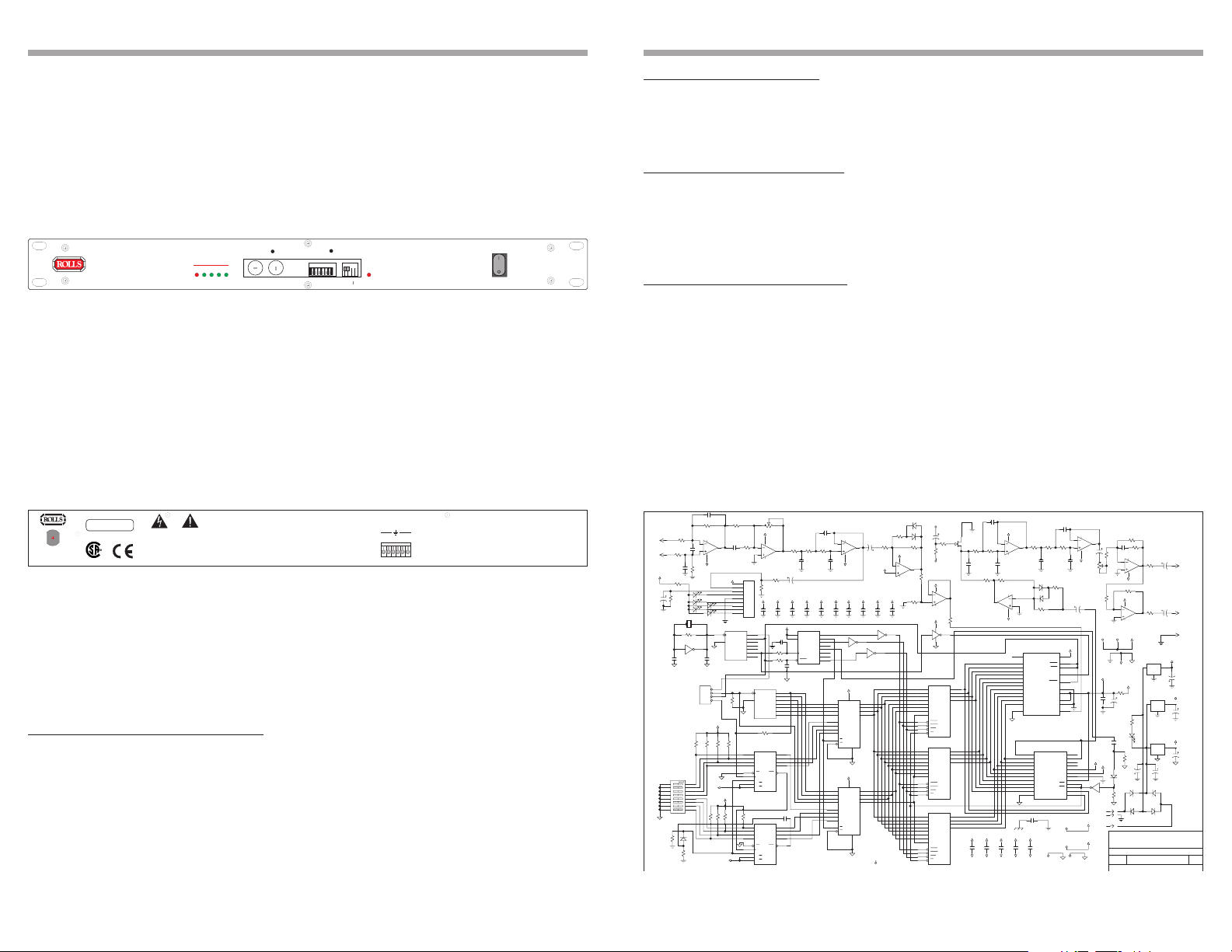
SCHEMA TIC
C13 120PF
H2B
R3 10K
R1
HD5
10K
2
2
10K 1%
C15
U1A
H2A
3
102
1
R2
HD5
4
R4
10K
C2
-12V
120PF
10K
+12V
R10
100
C11
10U
10
20
40
80
160
320
640
D5
R11
D6
10K
X1
D8
D9
3.2768
R36 1M
9 8
U9D 74HC04
C12
25PF
JP1
1
320MS
2
3
4
40uS
HEADER 4
HD4
R43
R45
R44
10K
10K
10K
SW1
5
1
16
2
15
3
14
4
13
5
12
6
11
7
10
8
9
SW D IP-8
DIPSW -8
D17
R56
10K
R52
1N4148
10K
R55
1K
100K TP
47K
C3
4560
.0056
1
+12V
9
8
7
6
5
D7
4
3
2
1
1
CLK
2
RST
U7
4024
C14
25PF
R42
10K
+5V
R51
10K
RES
+5V
+5V
R47
R46
10K
10K
+5V
IN
+12V
8
R7
R8
4560
6
R6
5
10K
U6
BA6144
12
Q1
11
Q2
9
Q3
6
Q4
5
Q5
4
Q6
3
Q7
1
CLK
2
RST
U11
4024
P04Q0
P112Q1
P213Q2
P33Q3
CI5CO
15
CLK
1
PE
9
B/D
10
U/D
R48
10K
P04Q0
P112Q1
P213Q2
P33Q3
CI5CO
15
CLK
1
PE
9
B/D
10
U/D
10K
10K
7
U1B
C4
.0012
R12
75K
C9
R13
1U
10K
+5V +5V +5V +5V +5V +5V +5V +5V
BP6
BP9
BP7
BP8
503
503
503
503
+5V
C10
A1QA
120PF
B2QB
U8
QC
QD
74HC 164
QE
CLK8QF
QG
R57 1K
CLR9QH
R37
C32 470PF
2K
12
Q1
11
Q2
9
Q3
6
Q4
5
Q5
4
Q6
3
Q7
R49
10K
6
11
14
2
7
U12
4029
470PF
C1
6
11
14
2
7
U13
4029
C6
.0056
4560
R9
2
10K
U2A
3
C5
4
120PF
-12V
BP10
BP11
BP13
503
503
503
3
4
1 2
5
6
U9A
74HC04
10
11
12
13
+5V
16
1A21Y
2A52Y
VCC
3A113Y
4A144Y
3
U14
1B
6
2B
10
74HC 157
3B
13
4B
1
A/B
15
G
GND
8
+5V
16
1A21Y
2A52Y
VCC
3A113Y
4A144Y
3
1B
6
2B
U15
10
3B
13
74HC 157
4B
1
A/B
15
G
GND
8
C7
1
10U
BP14
503
11 10
3 4
4
7
9
12
4
7
9
12
D1 1N 4148
+12V
R15
D2
10K
1N4148
R53
R14
R16
+12V
1M
8
4.7K
100K
4560
-12V
6
VREF
7
U2B
5
R17
10K 1%
+12V
8
6
U5B
+5V
+5V
503
U9E 74HC04
U9B
74HC04
-12V
5
BP16
R19
10K 1%
BP17
+5V
503
5 6
U9C
74HC04
7 14
FOR 1280M S U SE 4464 VREF
14
A0
13
A1
12
A2
11
A3
8
A4
7
A5
6
A6
10
A7
5
RAS
16
CAS
4
WE
1
G
14
A0
13
A1
12
A2
11
A3
8
A4
7
A5
6
A6
10
A7
5
RAS
16
CAS
4
WE
1
G
14
A0
13
A1
12
A2
11
A3
8
A4
7
A5
6
A6
10
A7
5
RAS
16
CAS
4
WE
1
G
P1
R5
C39
10U
Q1 J113
R54
1M
4560
7
R39
1K
2
D0
3
D1
15
D2
17
D3
U16
4416
2
D0
3
D1
15
D2
17
D3
U17
4416
2
D0
3
D1
15
D2
17
D3
U18
4416
BP1
503
C21
.0056
+12V
8
4560
R21
R20
6
10K
10K
U3B
5
C22
C20
120PF
.0015
R35
R34
10K
10K
4560
2
1
U5A
3
4
-12V
1
2
3
4
5
6
7
8
9
10
11
13
14
12
+12V +12V +12V +12V +12V
BP2
BP4
BP3
503
503
-12V -12V -12V -12V -12V
503
7
.0015
DRDY
D0
D1
D2
D3
D4
D5
D6
D7
D8
D9
D10
D11
VSS
1
2
3
4
5
6
7
8
9
10
11
R22
10K
C23
D3
1N4148
100K
U10
HI5812
VOUT
D11
D10
D9
D8
D7
D6
D5
D4
D3
D3
DGND12D1
C38
503
BP5
503
C24
.0056
R23
R24
10k
10K
C25
120PF
R32
10K
D4
1N4148
R33
24
VDD
15
OEM
23
OEL
22
CLK
21
STRT
20
VREF-
19
VREF+
17
VAA+
16
VAA-
18
VIN
RFB
RC
RB
U19
RA
VDDA
MA X502
VSSA
AGND
VREF
CS
WR
D0
9
14
7
OUT
R26
47K
4560
2
R25
1
C27
U3A
3
C26
10U
4
-12V
P2
100K TP
R29
10K
C30
10U
+5V
470PF
24
23
22
+12V
21
20
19
18
17
16
15
14
U9F
13
74HC04
E2
+5V
+5V
18
4.7K
.0056
2
3
+12V
6
U4B
5
VCC VDD +5V
VSS
R18
1K
C18
C8
10U
503
R50
10K
D15
LDRR
C31
-12V
D10
1N4148
1312
1N4001
R41
10K
1E1
1
1
E3
Title
Size:
Rb
Date:
R27
10K
4560
R28
1
U4A
51
4
-12V
R30
10K
8
4560
R31
7
51
7912
U29
2
I
G
1
+5V
7812
U21
1
I
7805
U22
1
I
R40
1K
C36
1000uf
D11
D12
1N4001
D14
D13
1N4001
1N4001
ROLLS CORPORATION
5143 South Main Street
Salt Lake City, UT 84107
DIGITAL DELAY RD320
Document Number:
C28
10U
4
C29
10U
5
H2E
HD5
3
H2C
3
O
C33
10U
O
G
C34
1U
2
+5V
O
G
C35
1U
2
Rev:
Sheet of
1
D
14-May-1999
 Loading...