

Page 1

VA-5
Sept, 2000
1
SERVICE NOTES
Issued by RES
First edition
SN00042 K6018405 Printed in Italy (AB00) (AD)
Copyright © 2000 by ROLAND CORPORATION
All rights reserved. No parts of this publication may be reproduced in any form whithout the written permission of ROLAND CORPORATION.
Specifications
Keyboard:61 keys, synthesizer action, velocity-sensitive
Controllers:Tempo/Data dial, D Beam Controller, Bender/Modulation Lever, Master Volume knob, Keyboard/Accomp Balance knob, M-FX knob
(Multi-effect control)
Tone generation:
PCM: 128-voice polyphonic, GM2/GS compatible, 32 multitimbral parts, 3,649 sounds (48MB worth of PCM samples) 116 Drum Sets incl. oriental Drum
sets.
Digital effects:Reverb (8 types), Chorus (8 types), Delay (10 types), Parametric EQ, M-FX (DSP, 89 types)
Arranger (automatic accompaniment):128 Music Styles in ROM, 64 Disk Link Styles from floppy disk, Disk User style (instant access to one Style on
Floppy disk), 16 Acoustic Styles, Style Orchestrator & Morphing. 8-track User Styles Composer, SMF-to-Style Converter
Memories: 128 User Programs, 4 programmable One Touch memories for each Style, 5 Super Tones memories for instant Tone access (with programmable User level)
Display: Backlit VGA Touch Screen (LCD), new graphic user interface with animated icons
Navigation: Virtual band (interactive Easy Routing), automatic and/or via button
Sequencer: Realtime SMF Player (with Minus-One function), Easy 2-track recorder, 16-track sequencer with extensive editing function, Song Header
Post Edit, Lyrics display
Data storage: Floppy disk drive (2DD/2HD), realtime load, File types managed: Styles, Song SMF, User Program, MIDI sets
Amplification: 25 + 25W output power, 2-way Bass Reflex System
Connections: Output (L/mono, Right), Input (L/mono, Right), Sustain, Foot pedal (expression), Foot switch, Foot Controller (FC-7), 2 x Phones
Power Supply: 100V~240 (universal)
Dimension: 1190(W) x 197 (H) x 406 (D) mm
Weight: 15, 5 Kg
Accessories: See details on Parts List
Options: PK-5 Dynamic MIDI Pedal, FC-7 Foot Controller, MSA/MSD/MSE series floppy disks (Roland & third-party), RH-25/50 Headphones, DP-2
Pedal switch, DP-6 Pedal switch (pino type), BOSS FS-5U Foot Switch, EV-5 Expression pedal, BOSS FV-300L Foot Volume/Expression pedal, KC100/300/500 Keyboard Amplifiers
va-5
v-arranger keyboard
TABLE OF CONTENTS Page
SPECIFICATIONS 1
LOCATION OF CONTROLS 2
EXPLODED VIEW (TOP) 3
EXPLODED VIEW (BOTTOM) 3
WIRING DIAGRAM 4
KEYBOARD PARTS LIST 5
PARTS LIST 5
HOW TO SAVE THE SYSTEM PROGRAM OR THE TEST PROGRAM ONTO FLOPPY DISK. 6
HOW TO UPDATE THE SYSTEM PROGRAM OR THE TEST PROGRAM BY FLOPPY DISK. 7
TEST MODE 7
CALIBRATION PROCEDURE TO REPLACE THE PITCH BENDER 10
HOW TO ENTER THE TOUCH SCREEN CALIBRATION 10
HOW TO INIZIALIZE THE FLASH AREA 11
HOW TO LOAD THE 6th LANGUAGE 11
BLOCK DIAGRAM 12
MAIN PCB ASSY 13
CIRCUIT DIAGRAM (MAIN PCB ASSY) 14
CIRCUIT DIAGRAM (MAIN PCB ASSY/Beam Control Block) / (MAIN PCB ASSY/Keyscan Block) 15
CIRCUIT DIAGRAM (MAIN PCB ASSY/Memory Bank Block) 15
CIRCUIT DIAGRAM (MAIN PCB ASSY/2nd Uart Contr. Block) / (MAIN PCB ASSY/LCD Contr. Block) 16
CIRCUIT DIAGRAM (MAIN PCB ASSY/FDC & IDE Contr. Block) 17
AUDIO PCB ASSY 18
CIRCUIT DIAGRAM (AUDIO PCB ASSY) 19
SUPER TONES PCB ASSY & CIRCUIT DIAGRAM 20
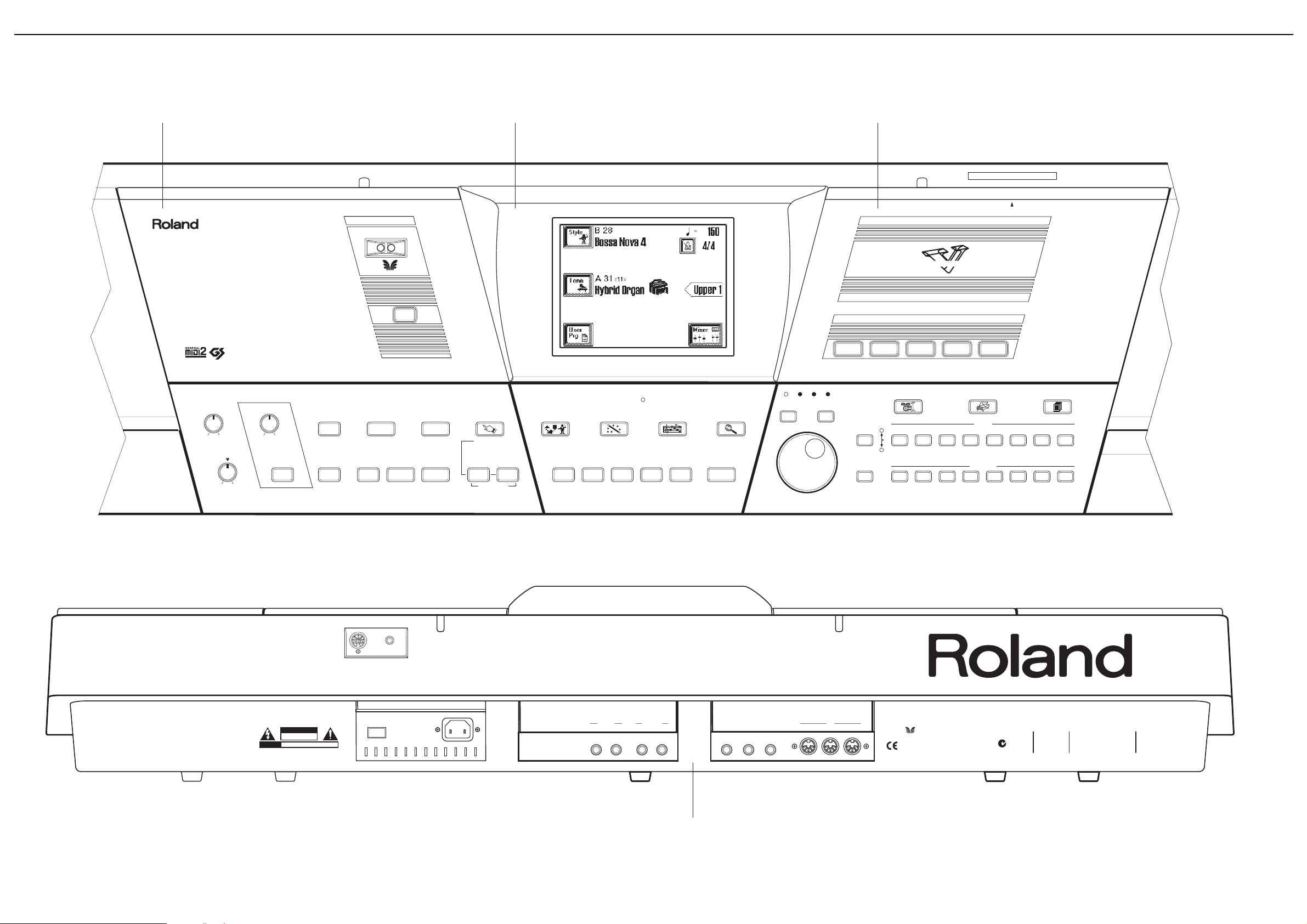
ATTENTION: The VA-5 is different from VA-7 only in some details such as, Top cabinet,
Keyboard assy ........... .
In this manual we have only listed the differences between the two instruments.
It is really necessary to refer to the VA-7 Service Notes for a deep knowledge
of this instrument.
Page 2
2
SUPER TONES
V-
Arranger
VA-5VA-5
V-ARRANGER KEYBOARD
128 VOICE POLYPHONY
V-ARRANGER KEYBOARD
128
VOICE POLYPHONY
KEYBOARD MODE USER PROGRAM
ORCHESTRATORONE TOUCH
INTRO ORIGINAL
BAND
VIRTUAL
COMPOSER
SONG
MENU
FUNCTION
STYLE
DATA
DISK
DATADATA
FREE PANEL
TEMPO
TEMPO
/ TAP
BANK
GROUP
PART
A
C
B
PIANO
REED PIPE SYNLEAD SYN PAD SYN SFX ETHNIC PERCUSSIVE SFX
CHR PERC ORGAN GUITAR BASS BRASS
O
RCHESTRAENSEMBLE
TONE USER PROGRAMUSER PROGRAM
EFFECTSCONTROLLERS
VOLUME
BALANCE
MIN MAX MIN MAX
KEYBOARD
ACCOMP
FILL VARIATION ENDING START/ STOP
NUMBER
MELODY
ON/OFF
ON/OFF
SYNC OTHER ARRANGER
PIANO DOWN UP
INTELL
1
1
2
2
334
4
5
5
66778
8
M-VALUE
M-FX
D BEAM CONTROLLER
1
2
34
5
POWER ON
TRANSPOSE
LCD CONTRAST
FC7 PEDAL
THRU
INOUTOUT
PEDALPEDAL
SWITCHSWITCHFOOTSWITCHFOOTSWITCH
RR L/MONOL/ MONO
MIDIFOOTFOOTSUSTAIN
STEREO OUTSTEREO
OUTSTEREO INSTEREO IN
AC
ATTENTION: RISQUEDE CHOC ELECTRIQUE NE PAS OUVRIR
CAUTIONCAUTION
RISK OF ELECTRIC SHOCK
DO NOT OPEN
N225
"THISCL ASS(B) DIGITAL APPARATUS COMPLIES WITH
CANADIANINTERFERENCE -CAUSING EQUIPMENT REGULATIONS“
"CETAPPAREIL NUMERIQUE DE LA CLASSE (B) RESPECTE LE
REGLEMENTSUR LE MATERIEL BROUILLEUR DU CANADA"
TheD Beam has been licensed by Interactive Light, Inc
WARNING:WARNING:
TO REDUCE THE RISK
OF FIRE OR ELECTRIC
SHOCK, DO NOT EXPOSE
THIS APPLIANCE TO
RAIN OR MOISTURE.
THIS DEVICE COMPLIES WITH PART 15 OF THE
FCC RULES. OPERATION IS SUBJECT TO THE
FOLLOWING TWO CONDITIONS: (1) THIS DEVICE
MAY NOT CAUSE HARMFUL INTERFERENCE, AND
(2) THIS DEVICE MUST ACCEPT ANY INTERFERENCE
RECEIVED, INCLUDING INTERFERENCE THAT MAY
CAUSE UNDESIRED OPERATION.
POWER ONPOWERON
VA-5
VARN.+ SILK. LEFT TEMPLATE F/TOP CBNT VA-5 VARN. COVER F/LCD VA-5
VARN.+ SILK. CONDUCTIVE BOTTOM CBNT VA-5
VARN.+ SILK. RIGHT TEMPLATE F/TOP CBNT VA-5
Cod. 7770311000
Cod. 7770307000
Cod. 7770308000
Cod. 7770310000
VA-5
Sept, 2000
LOCATION OF CONTROLS
REAR VIEW
Page 3
3
VA-5
Sept, 2000
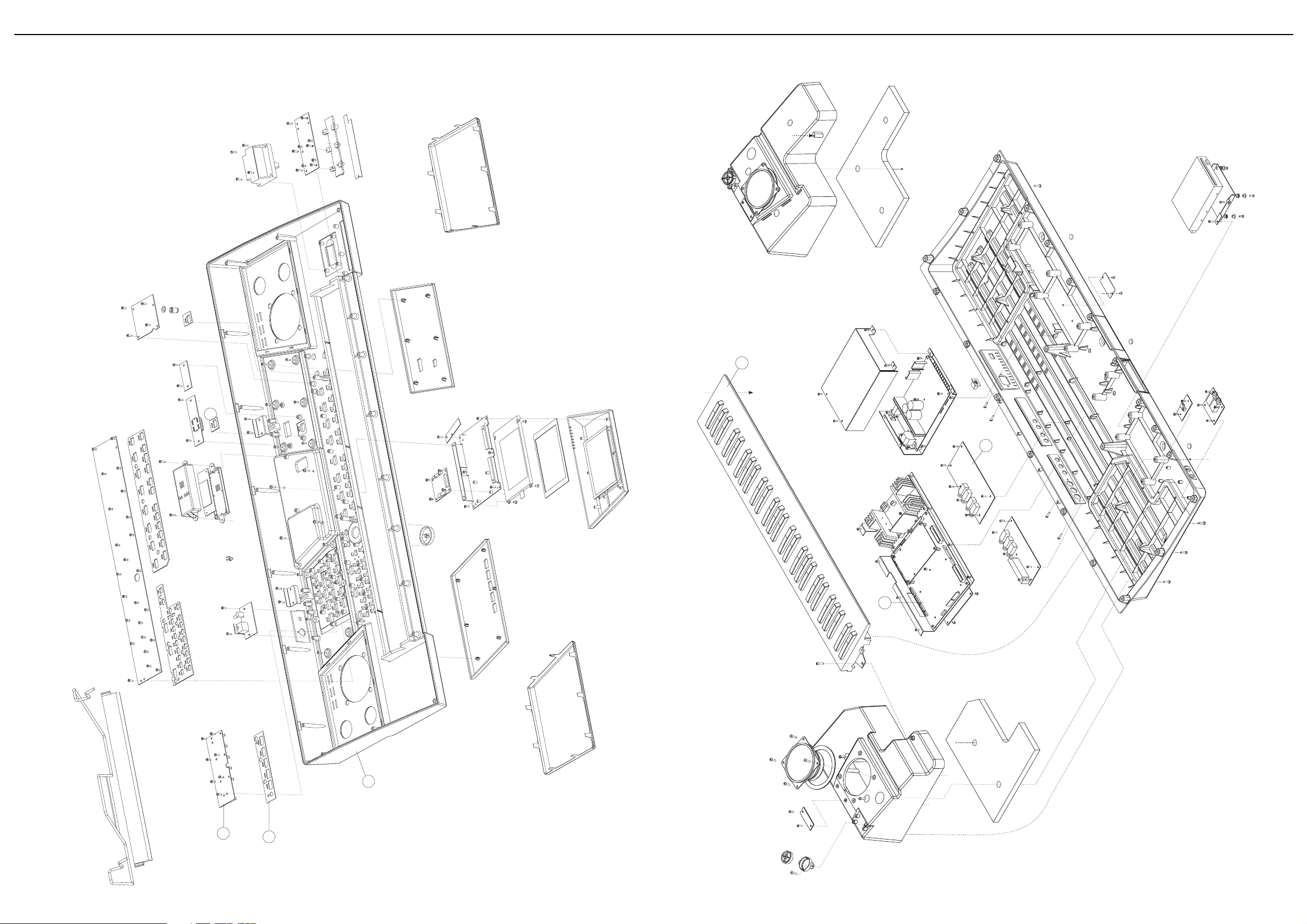
EXPLODED VIEW ( TOP)
1
2
3
2
PART LIST
No.
Part No. Description
1
7770309000
VARN. + SILK. TOP CABINET VA-5
2
3
7770303000
CONTROL SUPER TONES PCB ASSY VA-5
K2268167
VIBR. DUMPER F/TONES CONTROL BOARD VA-5
1
*
*
2
3
PART LIST
No.
Part No. Description
123
7626223001 61-KEY KEYBOARD ASSY VA-5TP/9
AUDIO PCB ASSY VA-57770302000
7770301000
MAIN PCB ASSY VA-5
EXPLODED VIEW ( BOTTOM)
Page 4
4
VA-5
Sept, 2000
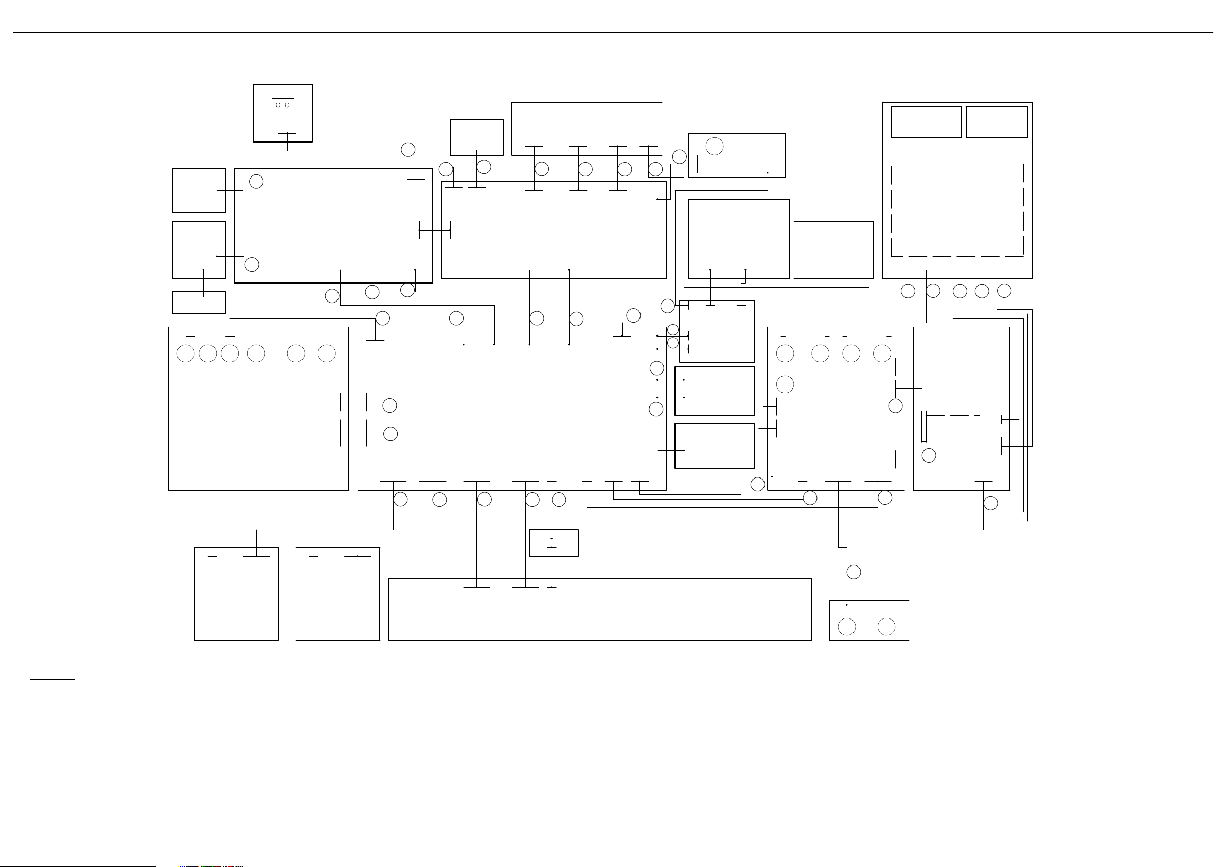
WIRING DIAGRAM
BENDER
LCD
KEYBOARD PCB
GRAPHIC
1/4 VGA
SWITCHING
POWER SUPPLY
SWM- 80
INLET
POWER
SWITCH
7
FDD
61 KEYS TP9
+5V
CFL LAMP
INVERTER
CXA-M10A-L
TDK
444
4
IN OUT THRU
EXPRESS.
PEDAL
FOOT
SWITCH
SUSTAIN
SWITCH
LCD
CONTRAST
DDD
JJJ
8
9
MIDI PCB ASSY
Volume
MAIN PCB ASSY
4
9
PCB ASSY
L(MONO) R
JJ
9
AUDIO
PCB ASSY
Volume
4
CN1
9
8
11
11
XPGS-6
PHONES
J
6
FC7 PCB ASSY
CN17
+5V
344
34 16
16
16
16
CN10
CN11
CN15CN16
6
9
6
3
8
8
CN2
CN1
CN1
12
CN4
11
53254-0410
CN2
53014-091053014-1110
5045-08A
5045-09A
5045-08 A
5045-09 A
53014-1210 53014-101053014-1110 53014-0410
53253-1110
34V P1.27 M AMPC1.2716P AMPC1.2716P
53014-0310
53014-0910
5045-09A5045-06A
53253-1110
CN1 CN2
CN11
CN12
CN4 CN9
10
CN1 CN4CN3 CN29
CN2
CN6
CN2
POTENTIOMETER
PCB ASSY
CONTROL PCB ASSY
MIDI STEREO OUT
CN2
6
5
7
CN5
7
5045-07A
CN10
CN1
4
SPEAKERS
7CN4
CN3
4
+17V
POWER
AMP. PCB
ASSY
7
CN1
53014-0710
4
CN6
L(MONO) R
JJ
STEREO IN
CN8
5045-05 A
CN6
AC
CN5 CN2 CN3 CN6
4
CN4
+5V
+5V;+12V;-1 2V
IDE
404
CN22
40
40V P1.27 M
CN21
CN2
53014-0410
53014-0710
7
RIBBON
5045-06A
5045-05A
5045-07A
5045-07A
5045-04A
5045-04A
EQU PCB ASSY
CN25
40KX14-40K11D
LCD CONTR.
PCB ASSY
CN24
7
B7B-PH-K- S
VARIPHRASE
5045-09 A
CN9
53014-0810 53014-1410
CN7 CN8
814
TOUCH SCREEN
CN7
CN1
52043-0410
006216012100808
CN23
53014-1310
13
13
CN2
53014-1310
7
B7B-PH-K- S
CN6
CN27
53014-0310
3
CN5
53014-0310
40
KX15-40K3 D
CN6
SUPER TONES
PCB ASSY
53014-0510
53014-0510
CN26
CN3
3
CN4
53014-0310
53014-03103
CN3
CN5
CN3
53014-1410
53014-081 0
5
CN2 CN3
12 11
53014-1210 53014-111 0
3
CN13
53014-0310
53014-1210 53014-111 0 53014-071 0
12 11 7
CN15 CN16 CN17
53014-0310
CN4
3
CN12
5
53014-0410
CN5
53014-0410
CN15
53014-0710
7
D.BEAM PCB ASSY
53014-0310
CN344
RIBBON
PCB ASSY
CN2
5597-08AP B
SWITCH
D.BEAM
PCB ASSY
4
4
53014-0410
53014-0410
CN11
CN1
53014-041053014-1210 53014-1010
CN7 CN8
53014-0810
CN10
53014-0810
11
5045-05 A
3
4
53014-0310
76382-404
AFTER TOUCH
I/F PCB ASSY
CN402
CN401
Aft
ZIP 100
PHONES
J
MIC/LINE I N
J
A
PCB ASSY
3
4
20
1
2
9
4
6
3
5
7
8
PHONES PCB ASSY
9
10
11
12
13
14
15
15 15
15
15
16
16
16
16
1818
18
17
17
17
19
19
19
21
19
22 25
23
24
26
17
X
X
X
X
X
X
X
X
X
X
X
1 00783234 BENDER CABLE (35) (W4PC P.2)
2 K3468155 4P CABLE 2R/2N (28) 2C D/R
3 K3468217 4P CABLE (72/96) -1C 4PC
4 K3468218 4P CABLE (72) -2C D/D
5 K2468106 7P CABLE (12) -2C D/R
6 K3468219 7P CABLE (32) -2C D/R
7 K3468171 9P CABLE (22) -2C D/R
8 K3468198 34P FLAT CABLE (18) -2C
9 J3469143 1P CONN. AWG18 (10) - YELLOW
10 7697212001 6P CABLE (64) -2C
11 7697220001 8P CABLE (32) -2C
12 7695108001 16P FLAT CABLE (24) -2C
13 7697223001 16P FLAT CABLE (38) -2C
14 K3468220 40P FLAT CABLE CM.18 -2C D/D (Only for VA-7)
15 7770304000 WIRING ASSY (W/3 CABLE ASSY) # NEW
16 7770118000 WIRING ASSY (W/4 CABLE ASSY)
17 7770117000 WIRING ASSY (W/5 CABLE ASSY)
18 7770119000 WIRING ASSY (W/3 CABLE ASSY)
19 7770305000 WIRING ASSY (W/3 CABLE ASSY # NEW
20 7698907000 4P CABLE ASSY (6) -2C P.2
21 7699415000 3P CABLE ASSY (44) -2C P.2 (Only for VA-7)
22 7770121000 3P CABLE ASSY 2V/1R (38) -2C 4P D/R (Only for VA-7)
23 7770122000 4P CABLE ASSY (32) 2C P.2 D/R (Only for VA-7)
24 7770123000 5P CABLE ASSY (12) -2C P.2 D/R
25 7770124000 3P CABLE ASSY 2N/1R (54) -2C 4P D/D
26 7700424000 11P CABLE ASSY (12) -2C P.2
NOTE: All the parts indicated with X do not exist on VA-5, but on VA-7 only.
Page 5
VA-5
Sept, 2000
5
CASING Q.ty
# 7770307000 VARN. COVER F/LCD VA-5 1
# 7770308000 VARN.+SILK.CONDUCTIVE BOTTOM CBNT VA-5 1
# 7770309000 VARN.+SILK. TOP CBNT VA-5 1
# 7770310000 VARN.+S. RIGHT TEMPLATE F/TOP CBNT VA-5 1
# 7770311000 VARN.+S. LEFT TEMPLATE F/TOP CBNT VA-5 1
KEYBOARD ASSY
# 7626223001 61-KEY TP/9 KEYBOARD ASSY 1
Note: If you have to use this keyboard on VA-5, you have to order the following parts together with the keyboard itself:
# K2158108 SUPPORT F/GROUND 1
# K2138113 SUPPORT F/KEYBOARD POSITIONING 1
J2289125 SELF TAP SCREW 2.9x10 TC TC PR TROP 2
J2289101 SELF TAP.SCREW 2.9X 6 TC TC 1
PCB ASSY
# 7770301000 MAIN PCB ASSY VA-5 1
# 7770302000 AUDIO PCB ASSY VA-5 1
# 7770303000 CONTROL SUPER TONES PCB ASSY VA-5 1
WIRING, CABLE
# 7770304000 WIRING ASSY (W -3 CBL ASSY) VA-5 For details refer to WIRING DIAGRAM on page 4. 1
# 7770305000 WIRING ASSY (W -3 CABLE ASSY) VA-5 1
# 7770306000 5P CABLE (8) -2C P.2 D/R VA-5 1
PACKING
# K2618236 OUTER PACKING VA-5 1
MISCELLANEOUS
# K2268167 VIBR. DUMPER F/TONES CONTROL BOARD VA-5 1
ACCESSORIES
# K2378118 USER PROGRAM/STYLES DISK VA-5 1
# K2378119 DEMO/STYLES DISK VA-5 1
E
PARTS LIST VA-5 (100V/117V/230V/230VE/240VA)
When ordering any parts listed in the parts list,please specify the following items in the order sheet.
QTY PART NUMBER DESCRIPTION MODEL NUMBER
Ex. 10 22575241 Sharp Key C-20/50
15 2247017300 Knob (orange) DAC-15D
Failure to completely fill the above items with correct number and description will result in delayed or
even undelivered replacement.
CONSIDERATION ON PARTS ORDERING
NOTE:
#
The parts marked " # '' are new (Initial Parts).
A The parts marked " A '' are new (Initial Parts).for RES but already used by RJA
The parts marked have Safety - Related characteristics.
Use only listed parts for replacement.
<< EMI >> Component for EMC.
NNoott ee :: Replacement should be made on a unit basis. No replacements available for individual parts.
Replacement only be a unit.
!
!
SAFETY PRECAUTIONS :
The parts marked have
safety-related characteristics.
Use only listed parts for
replacement.
!
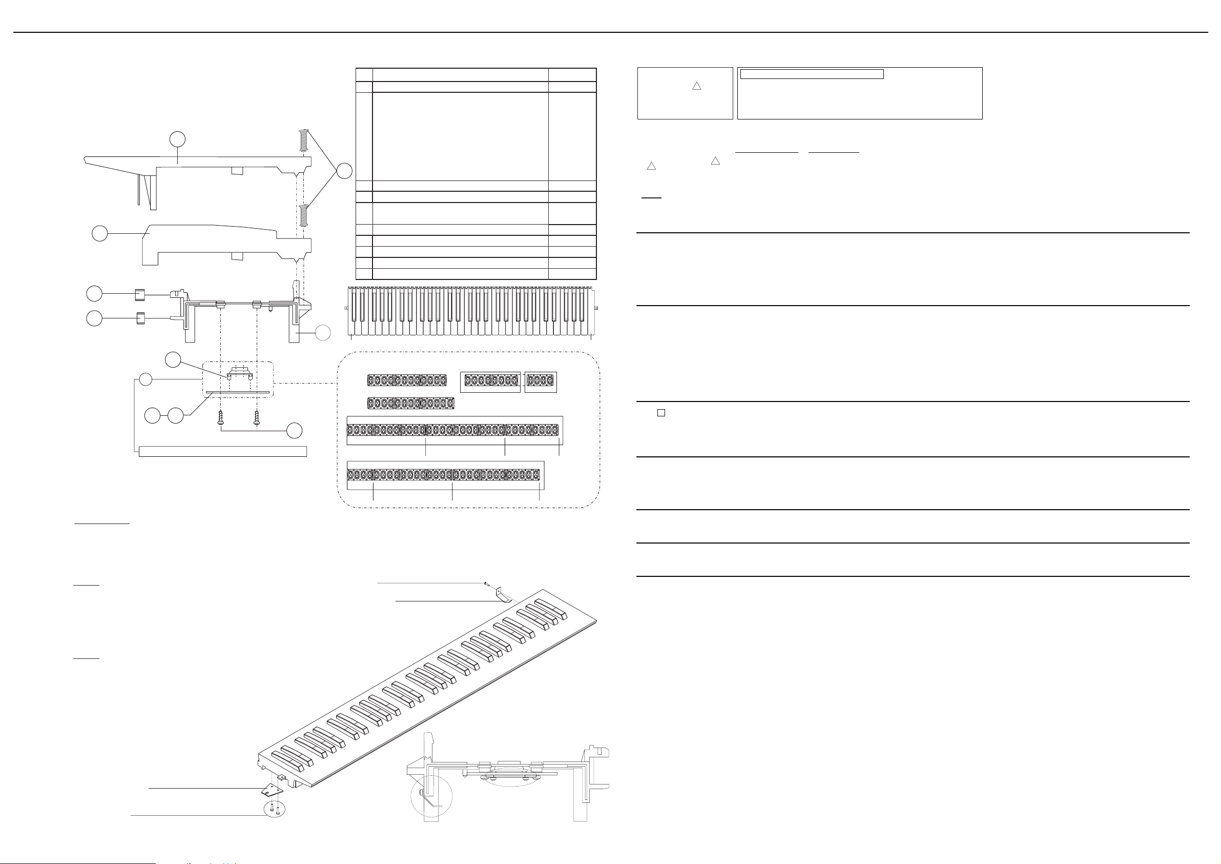
KEYBOARD PARTS LIST
61 KEY TP9 KEYBOARD ASSY
code 7626223001
1
2
3
8
10
9
PM
SM
5
76
4
1
2
3
4
5
6
7
8
9
10
PARTS NAME
KEY SPRING
NATURAL KEY C5 DO
RE
MI
FA
SOL
LA
SI
DO(F)
NATURAL KEY D6
NATURAL KEY E7
NATURAL KEY F1
NATURAL KEY G2
NATURAL KEY A3
NATURAL KEY B4
NATURAL KEY C8
SHARP KEY
SELF TAP SCREW 2.9x10 TC TC PR TROP
12P RUBBER CONTACT
13P RUBBER CONTACT
LEFT CONTACT PCB ASSY+RUBBER CONTACT
RIGHT CONTACT PCB ASSY+RUBBER CONTACT
PLASTIC CHASSIS
GUIDE BUSHING INFERIOR
GUIDE BUSHING SUPERIOR
CODE
22178233
22578319
22578328
22578329
22578330
22578331
22578332
22578333
22578334
22578335
J2289125
2218523801
2218523901
7624505001
7624504001
22818761
J2359104
22158789
N
O.
LEFT
RIGHT
A
C
A
AD
B
12 P RUBBER CONTACT
ASSEMBLY OF RUBBER CONTACT
13 P RUBBER CONTACT
A
D
BC
8P
4P
CONTACT BOARDS ARE COMPLETE WITH RUBBER CONTACTS
*
*
DO
DO(F)
Pict.1
Pict. 2
SUPPORT F/GROUND
POSITIONING
SUPPORT FOR KEYBOARD
Cod. K2158108
Cod. K2138113
Pict. 2
Pict. 1
SELF TAP SCREW 2.9x10 TC TC PR TROP
Cod. J2289125
SELF TAP.SCREW 2.9X 6 TC TC
J2289101
Cod.
CAUTION:
When you replace the keyboard on VA-5, please remember to modify it as shown in pictures 1 and 2, using the items below, that
you have to order together with the keyboard itself (see Parts List VA-5/Keyboard Assy).
Pict. 1
Pict. 2
:
Remove the copper strip placed on the back of the keyboard you have
received as replacement part.
Mount the SUPPORT F/GROUND (K2158108) at its place
.
:
Mount the SUPPORT F/KEYBOARD POSITIONING
left side of the keyboard, using the SELF TAP SCREW 2.9x10 TC TC
PR TROP (J2289125)
, using the
SELF TAP.SCREW 2.9X 6 TC TC (J2289101)
(K2138113) on the
Page 6
6
VA-5
Sept, 2000
HOW TO SAVE - HOW TO VERSION UP
Since VA-5 has a flash memory for the System program registration, you can update:
-the System program or the test program by floppy disks
Item Required
VA-5 System Program up disk (code: 7770313000)
VA-7/5 Test program disk (code: 7770134000)
ATTENTION:
The Test program was not installed in this instrument (otherwise it would have occupied too much memory
space).
If you want to install it, you have to load the Test Program from the "VA-5 Test program disk" you've been
provided with.
WARNING:
Loading the Test Program causes the System Program of your VA-5 to be lost. Therefore every time
you want to carry out some checks in your VA-5 and consequently have to install the related Test Program,
we strongly recommend you to make a back-up copy of your VA-5 current System program, according to
the procedure described in the << How to save the System Version or the Test Program onto Floppy disk >>
paragraph.
Of course, once you've completed your checks, you'll have to reload the System Program (that had been erased
when installing the Test Program), as described in the << How to update the System Program or the Test
Program by floppy disk >> paragraph.
How to visualize the System Program version
Turn the instrument on while keeping the [PIANO + ONE TOUCH + INTRO] buttons pressed, the display shows:
You can check the instrument software version, pressing the [BANK/1] button.
After a few seconds the display shows:
To exit from this screen display, turn the instrument off.
VA -5 Virtual Arranger
Ver. XX . XX
Day Month Day no. Time Year
CPU Bios Version: Ver. XX . XX
Flash : xxxxxxxx Size : xxxxxxx byte
***SYSTEM MENU***
BANK1: SYSTEM VERSION
BANK2: SYSTEM LOAD
BANK3: SYSTEM SAVE
How to save the System program or the Test Program onto Floppy
Disk.
Insert a formatted Floppy Disk in which youll save either the System Program or the Test Program
Turn the instrument on while keeping the [PIANO] + [ONE TOUCH] + [INTRO] buttons pressed.
The display shows:
Choose in the menu the option SYSTEM SAVE pressing [BANK/3] button
The display shows:
Choose in the menu the option CONTINUE pressing [NUMBER/1] button
The display shows:
Then after a few seconds the display will show:
When the program saving operation has been completed it will be confirmed by the System saving COMPLETED message appearing on the display.
To go back to the initial program, after a few seconds you have to turn the instrument off and then on again.
***SYSTEM SAVE***
System size [ BYTE ] XXXXXXX
Checksum Calculation ...... DONE
System saving ...... COMPLETED
<< TURN THE INSTRUMENT AGAIN >>
***SYSTEM SAVE***
System size [ BYTE ] XXXXXXX
Checksum Calculation ...... DONE
System saving ...... XXXXXXX
ATTENTION ! ! Do not turn instrument off
***SYSTEM SAVE***
NUMBER1: CONTINUE
NUMBER2: EXIT
***SYSTEM MENU***
BANK1: SYSTEM VERSION
BANK2: SYSTEM LOAD
BANK3: SYSTEM SAVE
Page 7

VA-5
Sept, 2000
7
How to update the System program or the Test program by Floppy disk
Insert the floppy disk containing either the System program (VA-5 System program up disk code 7770313000)
or the Test program (VA-7/5 Test program disk code 7770134000) into the FDD.
Turn the instrument on while keeping the [PIANO] + [ONE TOUCH] + [INTRO] buttons pressed.
The display shows:
Choose in the menu the option SYSTEM LOAD pressing [BANK/2] button
The display shows:
Choose in the menu the option CONTINUE pressing [NUMBER/1] button
After a few seconds, the display shows:
If the loading operation of the Flash has been completed, youll have the confirmation if the message COMPLETED is displayed.
After a few seconds, you have to turn the instrument off and then on again.
TEST MODE
After loading the Test program, turn the instrument on while keeping the [BANK/ 5] button pressed.
When the display shows: MODEL SELECTION, press [BANK/2] button.
The Test Menu will be displayed, which is divided into two major groups: BANK and NUMBER.
VA-7/5 test Ver. x x . x x
-BANK- -NUMBER1 Switch 1 Flash
2 Encoder 2 Rom Style
3 Adc 3 Ram
4 Lcd 4 Free
5 Led 5 FDD
6 Keyscan 6 Midi
7 Touch screen 7 Audio Test
DATE: (day) (month) xx xx:xx:xx (year)
***SYSTEM LOAD***
Program loading ...... ------------------
Program checking ...... ------------------
Flash updating ...... ------------------
<< TURN INSTRUMENT ON AGAIN >>
***SYSTEM LOAD***
NUMBER1: CONTINUE
NUMBER2: EXIT
***SYSTEM MENU***
BANK1: SYSTEM VERSION
BANK2: SYSTEM LOAD
BANK3: SYSTEM SAVE
First group of test => BANK
1. SWITCH test
Press the [BANK/1] button, the display shows:
Action: every button, when pressed, will generate a sound. The LCD will consequently show the button name
on the top of the left side as well as its ON/OFF status. On the bottom of the left side the name of the following
button to be pressed will be shown. Every time a button has been checked, the asterisks disappear from the
display.
Once all buttons of the control panel and of the FC7 pedalboard have been subsequently pressed, you will
automatically exit the Switch Test and get back to the Test Menu.
If the Switch test has been already carried out previously and you want to exit it, you can do it by pressing the
Bank 8 button first and then the Bank 5 one.
2. ENCODER check
Press the [BANK/2] button, the display shows:
Action: A value (here represented by XXX) will be visualized in the upper right corner of the LCD.
Moving the encoder rightwards, this value will increase up to +255. Moving the encoder leftwards, it will
decrease until 0.
To exit, press [BANK/5].
3. ADC Check
Press the [BANK/3] button, the display shows:
Action: The LCD visualizes the values of the functions you are testing. These values vary from 0 to +127 or to
-127.
To exit, press [BANK 5].
VA-5 ADC TEST
Bender (0 +/- 127) D.Beam C. (0 - 127) **
Modulation (0 - 127)
Ribbon (0 - 127) Sust Foot switch (On/Off )
Balance (0 +/- 127) Foot switch (On /Off)
M - FX (0 + 127) Express (0 - 127)
Press BANK 5 to exit
VA-5 TEST ENCODER
ENCODER
ÞÞ
XXX
Press Bank 5 to exit
VA-5 SWITCH TEST
Nome XXXXX
O N /OFF
*****************************************
*****************************************
******************
Next. XXXXX
Press Bank 8 and Bank5 to exit
Page 8

8
VA-5
Sept, 2000
4.
LCD Check
Press the [BANK/4] button, the display shows:
Action:
If you press the [BANK/1] button, the display will be blue
If you press the [BANK/2] button, the display will be white;
If you press the [BANK/3] button, the display will be gray;
If you press the [BANK/4] button, the display will show some numbers (normal)
If you press the [BANK/6] button, the display will show an image
To exit, press [BANK/5].
5. LED Check
Press the [BANK/5] button.the display shows:
Action:
If you press the [BANK/1] button, all orange leds light
If you press the [BANK/2] button, all green leds light
If you press the [BANK/3] button, all red leds light
If you press the [BANK/4] button, all the leds light
If you press the [BANK/6] button, all the leds light in sequence
Note: All the LEDs will light one after the other and, at the end of the sequence, they will all light.
To exit, press [BANK/5].
6. KEYSCAN Check
Press the [BANK/6] button, the display shows:
Action: a piano sound will be heard every time a key is pressed; youll hear the aftertouch effect if you press a key till
the end of its stroke. The LCD shows the key name, the velocity value, the number of the octave used and the After
touch value.
To exit, press [BANK/5].
VA-5 KEY SCAN TEST
Key = C
Velocity = 0/127
Octave = 2
After Touch = 0/127
Press BANK5 to exit
VA-5 LED TEST
Press BANK 1 to orange colors
Press BANK 2 to orange colors
Press BANK 3 to orange colors
Press BANK 4 All led ON
Press BANK 6 Sequence ON
Press BANK5 to exit
VA-5 LCD TEST
Press BANK 1 blue Test
Press BANK 2 white Test
Press BANK 3 gray Test
Press BANK 4 normal Test
Press BANK 6 image Test
Press BANK5 to exit
7. TOUCH SCREEN Test
Note: to carry out this test, a normal pen is required.
Press the [BANK/6] button, the display shows:
BANK1 - calibrate
Action : Pressing the [BANK/1] button, you enter the Calibration test.
Action: Pressing the [BANK/1] button, you exit the Calibration test.
Pressing the [BANK/2] button, you enter the LCD calibration test.
Note: Once you enter the Calibration test, you can not exit unless you carry out the calibration operations.
The display shows:
Touch the left lower corner of each slit with the pen for a few seconds, according to the numbering shown in
the following picture. When the VA-5 recognizes the touch, + will change into 0.
This way, the writing Touch me will appear to show the correct order, so please follow this indication. During
the calibration, do not touch any point except "Touch me". After touching the four points, the calibration ends
and the display will show one of the following displays:
Note: The calibration set will be memorized on the VA-5 internal flash, by turning it on while keeping the
[Melody Intelligence] button pressed, after having loaded the System program.
When the calibration fails, the following display will appear.
Calibration OK
Press BANK5 to exit
VA-5 TOUCH SCREEN TEST
BANK1 - Exit calibrate
BANK2 - Confirm calibration
Press BANK5 to exit
VA-5 TOUCH SCREEN TEST
BANK1 - calibrate
BANK2 - touch X, Touch Y test
Press BANK5 to exit
4
+
+
2
Touch Me.
1
+
+
3
Page 9

VA-5
Sept, 2000
9
You have to carry out the calibration again.
Press the [BANK/5] button to go to the next test.
BANK2 - touch X, Touch Y test
Action : Pressing the [BANK/2] button, you enter the test to check the LCD "darkest" area, the display shows:
Action: Touch with a pen the upper left corner of the LCD in its darkest area. Pass the pen through the LCD,
horizontally first (from the left to the right) and check that the X value is 320. Then repeat the operation from
downwards to upwards and check that the Y value is 240. The acceptable variation from these values is +/- 5%.
To exit, press [BANK/5]
Second group of test => NUMBER
1. FLASH test
Press the [NUMBER/1] button, the display shows:
Action: The display visualizes the 24 blocks written and then verified in the flash.
OK will be visualized if everything works properly.
ERROR will be visualized if there are any anomalies.
To exit, press [BANK/5]
Note: if there is an asterisk (*) beside the Flash Test item within the Main Menù, this means that this kind of
check has already been carried out.
2. ROM STYLE Test
Press the [NUMBER/2] button the display shows:
To exit, press [BANK/5]
ROM STYLE TEST
OK or ERROR
Press BANK 5 to exit
VA-5 FLASH TEST
Writing 24
Verifying 24
Flash OK or Error
Press BANK 5 to exit
Touch X - 1
Touch Y - 1
Press BANK5 to exit
NG. Calibration
3. RAM Test
Press the [NUMBER/3] button, the display shows:
To exit, press [BANK/5]
4. Free
5 FDD Test
Press the [NUMBER/5] button the display shows:
After a few seconds, the display will show:
Action: If the floppy disk has not been inserted in the drive, the following writing will be visualized on the bottom of the lcd: PLEASE INSERT DISK.
If the result isnt OK, one of the following errors will appear on the display:
- Read Error
- Write Error
- Verify Error
CAUTION: To check the FDD, use only a formatted disk, either DD or HD type.
To exit, press [BANK/5]
VA-5 FDD TEST
Writing...
Reading...
Verifiyng
>>>> OK <<<<
Press BANK 5 to exit
VA-5 FDD TEST
Writing...
Reading...
Verifiyng
>>>> OK <<<<
Please eject disk
RAM TEST
OK or ERROR
Press BANK 5 to exit
Page 10

10
VA-5
Sept, 2000
6
MIDI & THRU test
Press the [NUMBER/6] button, the display shows:
Cable connections to check the MIDI outputs:
IN/OUT Connection THRU/IN connection
While the VA-5 MIDI TEST screen display is shown, connect the Midi Cables between VA-5 and an external
instrument as shown in the above diagram.
Make sure that either the OK or the ERROR message appear on the display.
Then keep the cable connection between the IN and OUT sockets of VA-5 and connect VA-5 with another
external instrument by using its Midi Thru output and the second Midi Cable.
If the result of this Midi Test is OK, youll hear an intermittent sound coming from the second external instrument.
To exit, press the [BANK/5].
7 Audio T
est
Press the [NUMBER/7] button. Youve entered the Audio Test mode and the display shows:
Pressing the [Bank/1] button "Calibration", some sine wave sounds (frequency 415 Hz) will come out from the
Right and Left speakers.
Before calibrating the amplifier, move the volume potentiometer to the Max position then adjust the trimmers of
the amplifier channels (VR11: right Channel; VR12: left Channel) so that the oscilloscope will show a value of 20
Vpp across the speakers.
Note: The measurements on the R/L output have to be carried out with the jacks inserted in both outputs .
The sounds coming from the R/L Mono channels on the OUT output will be mixed and can be adjusted by the
Volume slider potentiometer.
The sine wave sound on the right and left channels will have a 415 Hz frequency and a 3Vpp amplitude.
Pressing the [BANK/2] - Left button, a sine wave sound will be heard from the left loudspeaker, with a frequency of 215 Hz.
Pressing the [BANK/3] - Right button, a sine wave sound will be heard from the right loudspeaker, with a frequency of 215 Hz.
To exit, press [BANK/5].
VA-5 Audio Test
BANK 1 Calibration
BANK 2 Left
BANK 3 Right
Press BANK 5 to exit
In Out Thru
External Instrument
In Out Thru
Rear side of VA-5 bottom cabinet
VA-5 MIDI TEST
Connect Midi Out = to => Midi A In < OK or Error >
Press BANK5 to exit
CALIBRATION PROCEDURE TO REPLACE THE PITCH BENDER
Load the System Program into the instrument. Turn VA-5 on while keeping the [ORCHESTRATOR] button
pressed.
After a few seconds, the display will show:
Put the Bender lever in the middle while pressing the M-FX [ON/OFF] button at the same time.
The display shows:
Move the Bender lever completely towards left while pressing the M-FX [ON/OFF] button at the same time.
The display shows:
Move the Bender lever completely towards right while pressing the M-FX [ON/OFF] button at the same time.
When the calibration has been completed, the instrument will automatically reset and go back to the initial
screen display of the software program.
HOW T
O ENTER THE TOUCH SCREEN CALIBRATION
Turn the instrument on while keeping the [SONG COMPOSER] button pressed.
Note: When entered the Calibration test, you cannot exit unless you carry out the calibration operation.
To perform this test, a normal pen is required.
Press the left lower corner of each slit with the pen for a few seconds, according to the numbering shown in
the following picture.
When the VA-5 recognizes the touch, + will change into 0.
PITCH BENDER CALIBRATION
ALL RIGHT POSITION
Then Press M-FX on/off Key
PITCH BENDER CALIBRATION
ALL LEFT POSITION
Then Press M-FX on/off Key
PITCH BENDER CALIBRATION
CENTER POSITION
Then Press M-FX on/off Key
Page 11

VA-5
Sept, 2000
11
This way, the writing Touch me will appear to show the correct order, so please follow this indication.
During the calibration, do not touch any point except "Touch me". After touching the four points, the calibration
ends and the display will show one of the following displays:
If Calibration OK appears, the instruments will reset and get back to the normal working display.
Note: The calibration set will be memorized on the VA-5 internal flash, by turning it on while keeping the
[MELODY INTELL.] + [CONTROLLERS] + [EFFECTS] buttons pressed.
If the calibration fails, the following display appears.
You have to carry out the calibration again.
HOW TO INIZIALIZE THE FLASH AREA
Turn the instrument on while keeping the [MELODY INTELL.] + [CONTROLLERS] + [EFFECTS] buttons pressed.
After a few seconds, the display shows:
When the saving operation has been completed, the instrument will exit and get back to the VA-5 initial
display.
FLASH PARAMETER LOAD
WAIT PLEASE
NG. Calibration
Calibration OK
HOW TO LOAD THE 6th LANGUAGE
Turn the instrument on while keeping the [VIRTUAL BAND] button pressed.
The display shows:
Insert the floppy disk containing the XXXXXXXX.lan file.
After a few seconds, the display shows:
Turn the instrument off and on again.
Caution:
Loading the 6th language will cause the loss of the Netherlands language.
Example:
USER LANGUAGE CUSTOMIZE
Completed
<<Turn instrument on again>>
USER LANGUAGE CUSTOMIZE
Insert disk, please...
4
1
+
Touch Me.
+
+
+
2
3
Page 12

A
B
C
D
E
F
G
H
I
L
M
N
O
P
Q
R
S
T
U
J
K
12345678910 12131415161718192021222324252627282930
12
11
VA-5
Sept, 2000
BLOCK DIAGRAM
XRST
10MHz
20MHz
ADDRESS BUS
DATA BUS
CS BUS
1
425
3 1
425
3 1
425
3
31231
231
2
12
3
1
2
3
1
2
8
7
3
2
4
5
1
8
7
3
2
4
5
1
1
425
3
76
8
Page 13

A
B
C
D
E
F
G
H
I
L
M
N
O
P
Q
R
S
T
U
J
K
12345678910 12131415161718192021222324252627282930
13
11
VA-5
Sept, 2000
MAIN PCB ASSY ASSY 7770301000
E
View from component side View from solder side
Page 14

A
B
C
D
E
F
G
H
I
L
M
N
O
P
Q
R
S
T
U
J
K
12345678910 12131415161718192021222324252627282930
14
11
VA-5
Sept, 2000
CIRCUIT DIAGRAM (MAIN PCB ASSY)
VCC
PMUX1
PMUX2
PMUX3
2ND_UART CONTR. BLOCK
XRD
XIPC
XIPCINT
XWRL
A[0..7]
D[0..7]
10MHz
XRST
SOUT3
SIN3
SOUT4
SIN4
LCD CONTROLLER BLOCK
D[0..7]
XRD
XWRL
YD
LP
XSCL
XD3
XD2
XD1
XD0
XRST
XLCD
10MHz
A0
DISPON DISP_CON
XLCDINT
KEYSCAN BLOCK
D[0..7]
A[0..1]
XRD
XWRL
XKEY
XKEYINT
XRST
10MHz
BEAM CONTR. BLOCK
BCLK
XRST
DBV
MEMORY BANK BLOCK
D[0..15]
XDWR
XRAS
XRD
XCASH
XCASL
XSTYLE
XRST
XFLASH
XWRL
RYBY
WPCNT
VPPCNT
A[0..21]
SWAP_ROM
FDC& IDE CONTROLLER BLOCK
XRD
XWRL
XFDC
XIDE
XFDCINT
XIDEINT
XDACK1
XDREQ1
XFDCDEND
A[0..3]
D[0..15]
XIDXINT
RDYCNTL
FDCCONT
A18
XFDCRST
XRST
GWAITIN
20MHz
AN4
AN5 AN7
AN5
AN3
AN4
XGWAIT XGWAIT
XCS4 XCS4
XCS2 XCS2
AN3
AN7
AN2
PB2 PB2
AN0
WVOUT WVOUT
AN1
AN2 AN1
10MHz
XIPCINT
AN0
AN4
XGINT
XKEYINT XGINT
WVOUT
XKEYINT
10MHz
20MHz
10MHz
SS3
SS2
SS1
SS0
SCD0
XGWAIT LS3 LLP
LS2
LS1
XCS4 LS0
XCS2
XSCNEN
XGINT LLP
MUTE
SCD0 SCD0 LS3
LS2
LS1
LS0
SS3
SS2
XIPCINT XIPCINT SS1
XLCDINT XLCDINT SS0
XSCNEN
20MHz
10MHz
SWAP_ROM
MUTE
WPCNT
XSTYLE XSTYLE
XSTYLE
WPCNT
RYBY
WPCNT
RYBY
RYBY
SWAP_ROM
XDREQ1
RDYCNTL
XFDCRST
XIDEINT
XIDXINT
FDCCONT
XIDEINT
XIDEINT
XFDCDEND
XFDCDEND
XFDCRST
DREQ0
XIDXINT
XDREQ1
RDYCNTL
FDCCONT
XFDCDEND
FDCCONT
XDREQ1
XFDCRST
RDYCNTL
GWAITIN
GWAITIN
TOUCH0
TOUCH1
TOUCH2
TOUCH3
TOUCH3
TOUCH2
TOUCH0
SCD7
SCD5
SCD2
SCD3
SCD3
SCD1
SCD7
SCD6
SCD6
SCD1
SCD3
SCD5
SCD7
SCD4
SCD4
SCD6
SCD2
SCD7
SCD1
SCD6
SCD4
SCD2
SCD5
DISPON
EXP3
EXP0
EXENCA
LP
YD
XD3
XD1
XD2
XD2
YD
XD0
XD0
LP
XD1
XSCL XSCL
XD3
EXENCA
EXENCB
EXENCB
RXD0
TXD1
TXD1
RXD0
TXD0
RXD0
TXD0
TXD1
TOUCH1
A20
A10
A0
XDWR
A3
XCASH
A20
A[0..3]
A0
XWRL
A17
A7
A5
A10
A[0..1]
A6
A6
A0
A13
XCASL
XRD
A2
A19
A18
A3
A8
A14
A20
A15
A4
XWRL
XWRL
XWRL
A8
A3
XRD
XRD
A16
XDWR
A13
A21
XRD
A15
A1
A20
A0
XWRL
A7
A7
A2
A2
A1
A[0..7]
A19
XWRL
XRAS
A18
XRD
A16
A5
A13
A19
XWRL
A4
XCASH XCASH
A14
XWRL
XWRL
XRD
XCASH
A2
A1
A12
A0
A10
A17
XRD
A17
A15
A8
XCASL
XCASL
A21
XRD
A6
A3
A9
A16
A5
A21
A18
A9
A11
A12
A11
XWRL
XRAS
A21
A12
XDWR
A4
A[0..21]
A19
A4
A18
XRD
XRAS
XWRL
A11
A9
XRAS
A5
A14
A1
XCASL
D[0..7]
D12
D1
D6
D0
D3
D3
D7
D9
D4
D1
D2
D5
D[0..7]
D15
D15
D14
D8
D1
D3
D0
D1
D3
D13
D2
D[0..15]
D0
D0
D14
D2
D9
D11
D[0..15]
D11
D15
D11
D7
D4
D8
D4
D5
D0
D12
D1
D1
D4
D8
D0
D12
D6
D2
D10
D5
D13
D7
D6
D10
D5
D9
D13
D14
D2
D10
D3
D7
D6
XFLASH
XIDE
XPORT
XFDC
XKEY
XWRH
XPORT
XLCD
XFLASH
XFLASH
XFDC
XKEY
XDACK1
XDACK1
XFDCXLCDINT
XDREQ0
XIPC
XPORT
XKEY
XIPC
XIDE
XWRH
XWRH
XLCD
XWRH
XIDE
XLCD
XIPC
XDACK1
D4
D5
D6
D7
PMUX1
PMUX2
PMUX3
PMUX3
PMUX2
PMUX1
AN6
AN6
XLCDINT
XSTYLE
AN5
TXD0
EXP0
EXP3
EXP1
EXP2
EXP1
EXP2
RXD1
RXD1
RXD1
20MHz
XRST
XRST
XRST
XRST
XRST
XRST
XRST
XRST
XRST
XRST
XRST
SCLK
SCLK
XKEYINT
XFDCINT
XFDCINT
XFDCINT
SCLK
5VD
5VD5VD
5VD
5VREF5VD
5VREF
5VREF
5VREF
5VREF
5VREF
5VREF
5VREF
5VREF
+12V -12V
5VD
5VD
5VD
5VD
5VD
5VD
5VD
+12V
5VREF
5VREF
-12V
-12V
+12V -12V 5VD
5VD
5VD
5VD 5VD
+12V
5VD
5VD
5VD
5VD
5VD
5VD
5VD
5VD
5VD
-12V
5VREF
5VD
5VD
-12V
+12V
5VD
5VD
5VD
5VD
5VD
5VD
5VD
5VD
5VD
5VD
5VD
5VD
C2
10/16s
D1
DA204K
21
3
D2
DA204K
21
3
D3
DA204K
21
3
D4
DA204K
21
3
D5
DA204K
21
3
D6
DA204K
21
3
D7
DA204K
21
3
D8
DA204K
21
3
C9
100nFs
C10
100nFs
C11
100nFs
C12
100nFs
C13
100nFs
C15
33/25s
C17
33/25s
R3
470s
C20
22pFs
C21
22pFs
C22
22pFs
C23
22pFs
C24
22pFs
C25
22pFs
C26
22pFs
C27
22pFs
C28
22pFs
C29
22pFs
C30
22pFs
C31
22pFs
C32
22pFs
C33
22pFs
C34
22pFs
C35
22pFs
C36
22pFs
C37
22pFs
R5 10Ks
R6 10Ks
C38
10/16s
C39
100nFs
C40
100nFs
C41
100nFs
C42
100nFs
RA3
4X10Ks
4 5
6
7
8
3
2
1
C45 NIU
R11
0s
R13 100s
R15 100s
R16 100s
R17 100s
C46
NIU
C47
NIU
C48
NIU
C49
NIU
C50
NIU
RA6
8X10Ks
4
5
6
7
8
9
3
2
1
RA7
8X10Ks
4
5
6
7
8
9
3
2
1
RA8
8X10Ks
4
5
6
7
8
9
3
2
1
RA9
8X10Ks
4
5
6
7
8
9
3
2
1
RA10
8X10Ks
4
5
6
7
8
9
3
2
1
RA11
4X10Ks
4 5
6
7
8
3
2
1
R40
NIU
L1
NIU
TP1
TP
L2
EXCCL4532U1
L3
EXCCL4532U1
L4 EXCCL4532U1
L5 EXCCL4532U1
L6 EXCCL4532U1
L7 EXCCL4532U1
L8 EXCCL4532U1
L9
EXCCL4532U1
IC5
M51953A
2
3
5
4
1
NC
GND
RES
CAP
VCC
R51
47s
R52
47s
R53 100s
R54 100s
R55
0s
SW1
NIU
C82
100nFs
RA18 4X47s
1 8
2 7
3 6
4 5
RA19 4X47s
1 8
2 7
3 6
4 5
RA20 4X47s
1 8
2 7
3 6
4 5
RA21 4X47s
1 8
2 7
3 6
4 5
RA22 4X47s
1 8
2 7
3 6
4 5
RA23 4X47s
1 8
2 7
3 6
4 5
RA24 4X47s
1 8
2 7
3 6
4 5
RA25 4X47s
1 8
2 7
3 6
4 5
RA26 4X47s
1 8
2 7
3 6
4 5
C85
100nFs
C86
100nFs
C87
100nFs
C88
100nFs
C89
100nFs
TP5
TP
L28 BK2125HM102
L29 BK2125HM102
L30 BK2125HM102
L31 BK2125HM102
L32 BK2125HM102
L33 BK2125HM102
L34 BK2125HM102
L35 BK2125HM102
L36 BK2125HM102
L37 BK2125HM102
L38 BK2125HM102
R94
0s
R95 0s
R34
NIU
R35
NIU
R36
NIU
C69
100uF25
C70
100uF25
C71
100/16s
C14
100nFs
C16
100nFs
C3
10nFs
C1
33/25s
R2
1Ks
R31
10Ks
R32 10Ks
R33
10Ks
R7
47s
R10
NIU
R12
NIU
R56 100s
C76
10nFs
RA32
4X10Ks
4 5
6
7
8
3
2
1
R110
0s
X1
20MHz
TP11
TP
R115 10Ks
RA17
4X47s
1 8
2 7
3 6
4 5
R4
10Ks
RA15
8X10Ks
4
5
6
7
8
9
3
2
1
RA4
4X10Ks
4 5
6
7
8
3
2
1
C93
33/25s
CN9
5045-09A
3
4
5
6
7
8
2
1
9
CN10
5045-09A
3
4
5
6
7
8
2
1
9
CN1
53014-1210
3
4
5
6
7
8
2
1
9
10
11
12
CN6
5045-08A
3
4
5
6
7
8
2
1
C8
100nFsC7100nFsC6100nFsC5100nFsC4100nFs
C18
12pFs
C19
12pFs
R50 1Ks
TP2
niu
TP3
niu
TP4
niu
TP7
niu
TP12
niu
IC8
74HC74
FLAT
2
3
1
4
12
11
13
10
5
6
9
8
14
7
D1
CLK1
CLR1
PR1
D2
CLK2
CLR2
PR2
Q1
Q1
Q2
Q2
VCC
GND
C75
220nF
16V 5%
RA5
4X10Ks
4 5
6
7
8
3
2
1
RA35
4X10Ks
4 5
6
7
8
3
2
1
L44
EXCCL4532U1
L45
EXCCL4532U1
L43
BK2125HM102
R41
4K7s
NIU
RA14
4X10Ks
4 5
6
7
8
3
2
1
C84
100nFs
L18
EXCCL4532U1
IC1B
UPC4570G
6
5
7
IC1A
UPC4570G
2
3
1
UPC4570G
8
4
CN24
B7B-PH-K-S
3
4
2
1
5
6
7
R1
100Ks
R151 100s
R152 100s
R153 100s
R154 100s
L51
EXCCL4532U1
IC40
74HC273
32
45
76
89
1312
1415
1716
1819
11
110
20
D1Q1
D2Q2
D3Q3
D4Q4
D5Q5
D6Q6
D7Q7
D8Q8
CLK
CLRGND
VCC
L26 BK2125HM102
L23 BK2125HM102
L25 BK2125HM102
L24 BK2125HM102
L21 BK2125HM102
L27 BK2125HM102
L22 BK2125HM102
RA12
4X100s
1 8
2 7
3 6
4 5
RA13
4X100s
1 8
2 7
3 6
4 5
C188
47/16s
RA45
4X100s
1 8
2 7
3 6
4 5
IC3
M60205-0601FP
22952
79
128334053
80
6
4
5
25
66
65
64
63
62
61
60
59
3
67
69
68
74
73
72
71
78
77
76
75
70
81
89
88
87
86
85
84
83
82
90
91
92
100
99
98
97
96
95
94
93
23
22
21
20
19
18
17
16
15
14
13
12
11
10
9
8
7
34
35
36
31
32
37
41
39
38
24
55
54
51
50
49
48
47
46
45
44
43
42
58
57
56
27
30
26
VDD
VDD
VDD
VDD
VSS
VSS
VSS
VSS
VSS
VSS
MIDI IN
WRHO
WRLO
WAIT IN
PORT7
PORT6
PORT5
PORT4
PORT3
PORT2
PORT1
PORT0
PWM 2
PWM 1
ENC B
ENC A
SS3
SS2
SS1
SS0
LS3
LS2
LS1
LS0
SSEN
LLCK
PD7
PD6
PD5
PD4
PD3
PD2
PD1
PD0
RS/CD
R/W
LE/RD
LCD 7
LCD 6
LCD 5
LCD 4
LCD 3
LCD 2
LCD 1
LCD 0
A21
A20
A19
A5
A4
A3
A2
A1
A0
D7
D6
D5
D4
D3
D2
D1
D0
XRD
XWRH
XWRL
XDREQ
XDACK
WAIT OUT
CS6
CS4
CS2
XIREQ
ECS11
ECS10
ECS9
ECS8
ECS7
ECS6
ECS5
ECS4
ECS3
ECS2
ECS1
ECS0
EXTINT2
EXTINT1
EXTINT0
CLK IN
CLK OUT
RESET
CN23
53014-1310
3
4
5
6
7
8
2
1
9
10
11
12
13
CN27
53014-0310
3
2
1
CN28
NIU
50
49
48
47
46
45
44
43
42
41
40
39
38
37
36
35
34
33
32
31
30
29
28
27
26
25
24
23
22
21
20
19
18
17
16
15
14
13
12
11
10
9
8
7
6
5
4
3
2
1
50
49
48
47
46
45
44
43
42
41
40
39
38
37
36
35
34
33
32
31
30
29
28
27
26
25
24
23
22
21
20
19
18
17
16
15
14
13
12
11
10
9
8
7
6
5
4
3
2
1
CN3
53014-1110
3
4
5
6
7
8
2
1
9
10
11
R14 100s
IC6D
74HC00
12
13
11
IC6B
74HC00
4
5
6
IC6C
74HC00
9
10
8
IC6E
74HC00
147
RA16
4X10Ks
4 5
6
7
8
3
2
1
R155
4K7s
CN4
53014-1010
3
4
5
6
7
8
2
1
9
10
TP19
TP
RA44
4X100s
1 8
2 7
3 6
4 5
R156
10Ks
R157
10Ks
CN29
53014-0410
3
4
2
1
R159
4K7s
R160 4K7s
TP20 TP
TP21 TP
CN11
NIU
5
7
9
11
13
15
3
1
17
19
21
23
25
27
29
31
33
35
37
3940
38
36
34
32
30
28
26
24
22
20
18
16
14
12
10
8
6
4
2
R161
NIU
R162
NIU
C203
NIU
C204
NIU
R158
10Ks
CN25
53014-1110
3
4
5
6
7
8
2
1
9
10
11
R108
10Ks
C206
NIU
C218
100nFs
R112
10Ks
R179 47s
IC43C TC7W34FU
3 5
R180 100s
IC44A TC7W34FU
1 7
IC44B TC7W34FU
6 2
R181 100s
R182 100s
R177 0s
IC43D
TC7W34FU
84
IC44D
TC7W34FU
84
L53
EXCCL4532U1
IC43A TC7W34FU
1 7
IC43B TC7W34FU
6 2
R178 100s
R8
10Ks
CN26
53014-0510
3
4
2
1
5
C217
100nFs
IC44C
TC7W34FU
3 5
IC42B
NIU
6 2
C185
NIU
C186
100nFs
C193
100nFs
CN2
NIU
3
2
1
C202
33/25s
C216
100/16s
C219
100/16s
RA1
8X10Ks
4
5
6
7
8
9
3
2
1
C205
NIU
RA2
8X10Ks
4
5
6
7
8
9
3
2
1
FL2
ELKS471FA
2
1 3
FL3
ELKS471FA
2
1 3
L52
NIU
IC42D
NIU
84
IC41D
NIU
84
C43
47pFs
IC7
TC7S32F
1
2
4
53
IC6A
74HC00
1
2
3
IC4
HD6437034ADxxx
{1ST PART FIELD}
7715437075
83
31222314052617296
48
102
101
100
98
95
94
93
88
87
107
108
109
110
47
46
45
44
42
41
39
38
37
36
35
34
33
32
30
29
28
27
26
25
24
23
21
20
19
18
17
16
14
13
11
10
9
8
7
6
5
4
76
97
92
90
89
86
91
2
1
112
111
69
66
67
68
65
64
106
79
73
74
71
78
84
99
56
55
82
81
54
53
80
51
50
49
62
60
59
58
57
63
85
105
104
103
VPP
VCC
VCC
VCC
VCC
VCC
VSS
VSS
VSS
VSS
VSS
VSS
VSS
VSS
VSS
CS0
PB4/TP4/TIOCA4
PB3/TP3/TIOCB3
PB2/TP2/TIOCA3
PB1/TP1/TIOCB2
PC7/AN7
PC6/AN6
PC5/AN5
PC1/AN1
PC0/AN0
PB8/TP8/RXD0
PB9/TP9/TXD0
PB10/TP10/RXD1
PB11/TP11/TXD1
A21
A20
A19
A18
A17
A16
A15
A14
A13
A12
A11
A10
A9
A8
A7
A6
A5
A4
A3
A2
A1
A0(HBS)
AD15
AD14
AD13
AD12
AD11
AD10
AD9
AD8
AD7
AD6
AD5
AD4
AD3
AD2
AD1
AD0
NMI
PB0/TP0/TIOCA2
PC4/AN4
PC3/AN3
PC2/AN2
AVREF
AVSS
IREQ7/TP15
IREQ6/TP14
IREQ5/TP13/SCK1
IREQ4/TP12/SCK0
IREQ3/DREQ1
IREQ0/DACK0
IREQ1/DREQ0
IREQ2/DACK1
PA11/TIOCB1
PA10/TIOCA1
VSS
RESET
EXTAL
XTAL
CK
WDTOVF
VCC
VCC
CS7/WAIT
CS6
MD2
MD1
CS5/RAS
CS4
MD0
CS3/CASL
CS2
CS1/CASH
PA8/BREQ
PA7/BACK
RD
PA5/WRH
WRL
PA9/IREQOUT/AH
AVCC
PB7/TOCXB4
PB6/TOCXA4
PB5/TP5/TIOCB4
R184 NIU
R185 NIU
NIU
C44
NIU
D10
NIU
1 2
C68
1uFs
R9
NIU
C178
22pFs
C220
22pFs
C221
22pFs
C222
22pFs
C223
22pFs
C224
22pFs
C83
100nFs
CN8
53014-1410
3
4
5
6
7
8
2
1
9
10
11
12
13
14
IC41A NIU
17
IC41B NIU
6 2
IC41C NIU
3 5
C227
NIU
C228
NIU
C229
NIU
C225
NIU
R164 NIU
R165 NIU
R163 NIU
CN7
53014-0810
NIU
3
4
5
6
7
8
2
1
C192
100nFs
C77
10nFs
IC39
TC7S32F
1
2
4
53
C201
47/16s
C226
NIU
IC42A NIU
1 7
R167 NIU
R166 NIU
IC42C NIU
3 5
EXPJ
EXPJ
Page 15

A
B
C
D
E
F
G
H
I
L
M
N
O
P
Q
R
S
T
U
J
K
12345678910 12131415161718192021222324252627282930
15
11
VA-5
Sept, 2000
CLK:
FREQUENCY:54.7KHz
DUTY:50%
PULSE:
DUTY:12.5%
FREQUENCY:6.84KHz
PULSE WIDTH:18.3uS
(AN4)
FLAT
FLAT
FLAT
FLAT
FLAT
DBV
PULSE
BEAM
PULSE
XDBPLS
XRST
CLK
A
A AA
A
A
A
D
D
D
D
D
AD
+12V
+12V
-12V
5VD
+12V
+12V 5VD-12V
5VD
-12V
-12V
D
5VD
D
5VD 5VD
5VD
A
-12V+12V
A
D
D13
DAN202K
21
3
D14
DAN202K
21
3
VR1
EVND8AA03B 24
13
2
D15
DAP202K
2 1
3
D12
DAP202K
2 1
3
R116
820KS
R117
68KS
R118
12KS
C160
47pFS
R124
120KS
R119
2K2S
C165
10pFS
R132
10KS
R140
NIU
R139
47KS
R138
47KS
R137
100S
TP
TP16
TP
TP
TP15
TP
C168
10nFS
R134
100S
R135
15KS
C166
100nFs
R136
33KS
C169
100nFs
C161
47nF
P.5 5%
R129
100 KS
R130
NIU
C163
15pFS
C164
100nF
P.5 5%
IC30
TC7SU04F
5
1
432
R126
1K5S
R128
33KS
Q7
2SA1037KR
2
1
3
R127
3K3S
CN21
53014-0710
3
4
2
1
5
6
7
R125
4K7S
C162
8200pF
P.5 5%
Q8
2SK368GR
3
1 2
C174
100nFs
R120
10KS
R121
68KS
R122
120KS
R123
1KS
R133
18KS
R131
1MS
D16
DA204K
CHIP
2 1
3
IC29B
74HC10
3
4
5
6
IC29C
74HC10
9
10
11
8
IC29D
74HC10
147
IC29A
74HC10
1
2
13
12
C173
100nFs
IC28B
74HC393
13 11
10
9
812
AQA
QB
QC
QDCLR
IC28A
74HC393
1 3
4
5
62
AQA
QB
QC
QDCLR
-
IC26A
UPC4570G
2
3
1
-
IC26B
UPC4570G
6
5
7
-
IC26C
UPC4570G
8
4
-
IC27A
UPC4570G
2
3
1
-
IC27B
UPC4570G
6
5
7
-
IC27C
UPC4570G
8
4
C177
100nFs
L42
EXCCL4532U1
L41
EXCCL4532U1
IC28C
74HC393
7
14
GND
VCC
C170
100nFs
C167
100nFs
C171
100nFs
C172
100nFs
C175
33uF25s
C176
33uF25s
XRST
BCLK
DBV
CIRCUIT DIAGRAM (MAIN PCB ASSY/ Beam Control. Block)
CIRCUIT DIAGRAM (MAIN PCB ASSY/ Keyscan Block)
To LEFT CONTACT BOARD
MK0 MK0 T0
BR0 BR0 T1
MK1 MK1 T2
BR1 BR1 T3
MK2 MK2 T4
BR2 BR2 T5
MK3 MK3 T6
BR3 BR3 T7
10MHz MK10 MK4
BR10 BR4
MK9 MK5
A1 BR9 BR5
A0 MK8 MK6
BR8 BR6
MK7 MK7
D7 BR7 BR7
D6 MK6
D5 BR6
D4 MK5 MK4 T0
D3 BR5 MK8 BR4 T1
D2 MK4 BR8 MK5 T2
D1 BR4 MK9 BR5 T3
D0 MK3 BR9 MK6 T4
BR3 MK10 BR6 T5
MK2 BR10 MK7 T6
XKEYINT BR2 BR7 T7
MK1 MK8 MK9
XRD BR1 BR8 BR9
XWRL MK0
XKEY BR0
T0
T7 T1
XRST T6 T2
T5 T3
T4 T4
T3 T5
T2 T6
T1 T7
T0
BR0 MK0
BR1 MK1
BR2 MK2
BR3 MK3
BR4 MK4
BR5 MK5
BR6 MK6
BR7 MK7
BR8 MK8
BR9 MK9
D
D
D
D D
D
5VD
5VD
CN15
3
4
5
6
7
8
2
1
9
20
19
18
17
16
15
14
13
12
1110
C96
33uF25s
CN16
AMPC1-2 716P
3
4
5
6
7
8
2
1
9
10
11
12
13
14
15
16
C98 NIU
C99 NIU
C100 NIU
C101 NIU
C102 NIU
C103 NIU
C104 NIU
C105 NIU
C106 NIU
C107 NIU
C108 NIU
C109 NIU
C110 NIU
C111 NIU
C112 NIU
C113 NIU
C97
4n7s
C95
100nFs
RA28
8X10Ks
4
5
6
7
8
9
3
2
1
RA27
8X10Ks
4
5
6
7
8
9
3
2
1
RA29
8X10Ks
4
5
6
7
8
9
3
2
1
RA30
8X10Ks
4
5
6
7
8
9
3
2
1
C152 NIU C153 NIU
C154 NIU C155 NIU
IC10
SSC1080F 0B
7
33
20
46
24
23
22
21
19
18
17
16
15
14
13
12
11
10
9
8
6
5
4
3
2
1
31
30
29
28
27
26
25
32
49
48
47
44
43
42
41
40
39
38
37
34
36
35
45
50
51
52
VDD
VDD
VSS
VSS
SC10
PR10
SC9
PR9
SC8
PR8
SC7
PR7
SC6
PR6
SC5
PR5
SC4
PR4
SC3
PR3
SC2
PR2
SC1
PR1
SC0
PR0
T7
T6
T5
T4
T3
T2
T1
T0
CLK
A1
A0
D7
D6
D5
D4
D3
D2
D1
D0
INT
RD
WR
CS
RESET
TEST1
TEST2
FL4
ELKS47 1FA
2
13
A[0..1]
D[0..7]
XRD
XWRL
XKEY
XRST
XKEYINT
10MHz
To RIGHT CONTACT BOARD
AMPC1-2 716P
DATA_BUS
ADDRESS_BUS
DRAM_CONTROL
ROM_CONTROL
FLASH_CONTROL
Vpp
XRST
XRAS XFLASH
RYBY
WPCNT
XWRL
XSTYLE
D4
A20
A12
A2
A6
A14
D12
D10
D10
A12 D5
A17
D6
A3
A1
D14
A9
D7
A19
D0
XCASH
D9
A7
D5
D11
D0
A18
A3
D14
A16
D12
D4
D2
A17
A4
D6
A18
A3
D13
A11
D10
D5
D3
D0
A5
D1
A20
A21
A1
A8
D3
A10
A5
A16
D8
D7
A19
XCASL
D9 D9
A9
A15
D7
D11
D11
A6
A11
D1
D2
A12
A11
D15
D15
A8
A13
A10
A14
D12
D8
A15
D6
A1
D8
D2
A7
A7
D1
A9
A2
D14
A6 D13
D13 A8
D3
A4
A5
D15
D4
A4
A13
A10
A2
XRD
XRD
XDWR
D
D
DD
5VD
5VD
5VD
5VD
5VD
D
L40
EXCCL453 2U1
R90
NIU
R93
22Ks
C147
33uF25s
C148
33uF25s
Q6
NIU
2
1
3
R89 0s
L39
EXCCL453 2U1
C146
100nFs
C145
100nFs
C144
100nFs
R91
NIU
C149
NIU
R92
NIU
C150
100nFs
IC20
TE28F160S570
16MBit FLASH ROM 65ns TSOP 56 pin
4
5
6
7
8
10
11
12
13
17
18
19
20
22
23
24
25
26
27
28
32
52
50
47
45
41
39
36
34
51
49
46
44
40
38
35
33
31
16
14
2
55
54
15
9
43
37
56
21
48
42
1
3
30
29
53
A20
A19
A18
A17
A16
A15
A14
A13
A12
A11
A10
A9
A8
A7
A6
A5
A4
A3
A2
A1
A0
DQ15
DQ14
DQ13
DQ12
DQ11
DQ10
DQ9
DQ8
DQ7
DQ6
DQ5
DQ4
DQ3
DQ2
DQ1
DQ0
BYTE
RP
CE0
CE1
WE
OE
VPP
VCC
VCC
VCC
WP
GND
GND
GND
3/5
NC
NC
NC
RY/BY
IC21
HM5118160CJ -6
16MBit DRAM 60ns SOJ 42 pin
17
18
19
20
23
24
25
26
27
28
14
30
13
1
4229
16
15
22
21
6
37
2
3
4
5
7
8
9
10
33
34
35
36
38
39
40
41
31
11
12
32
A0
A1
A2
A3
A4
A5
A6
A7
A8
A9
RAS
UCAS
WE
VCC
VSSOE
A10
A11
VSS
VCC
VCC
VSS
DQ0
DQ1
DQ2
DQ3
DQ4
DQ5
DQ6
DQ7
DQ8
DQ9
DQ10
DQ11
DQ12
DQ13
DQ14
DQ15
LCAS
NC
NC
NC
IC19
K5258164
64/32MBit Rom 100ns SOP44pi n
43
2
3
34
35
36
37
38
39
40
41
42
4
5
6
7
8
9
10
11
31
14
12
33
15
17
19
21
24
26
28
30
16
18
20
22
25
27
29
23
13
32
144
A19
A18
A17
A16
A15
A14
A13
A12
A11
A10
A9
A8
A7
A6
A5
A4
A3
A2
A1
A0
A-1(D15)
OE
CE
BYTE
D0
D1
D2
D3
D4
D5
D6
D7
D8
D9
D10
D11
D12
D13
D14
VDD
VSS
VSS
NCA20
C143
100nFs
FL6
ELKS47 1FA
2
13
A[1..21]
XRAS
XCASH
WPCNT
RYBY
XWRL
XRST
XFLASH
VPPCNT
XSTYLE
XCASL
SWAP_ ROM
D[0..15]
XRD
XDWR
CIRCUIT DIAGRAM (MAIN PCB ASSY/ Memory Bank Block)
Page 16

A
B
C
D
E
F
G
H
I
L
M
N
O
P
Q
R
S
T
U
J
K
12345678910 12131415161718192021222324252627282930
16
11
VA-5
Sept, 2000
DATA BUS
ADDRESS BUS
A7
A6
A5
A4
A3
A2
A1
A0
D7
D6
D5
D4
D3
D2
D1
D0
XWRL
XIPC
10MHz
SIN4
XRST
SOUT4
SIN3
SOUT3
XRD
D
D
D
D
D
5VD
5VD
5VD
C117
100nFs
RA31
8X10Ks
4
5
6
7
8
9
3
2
1
C118
33uF25s
C151
100nFs
IC22
TC7SU04F
5
1
432
RA34
4X390s
4 5
6
7
8
3
2
1
RA33
4X10Ks
4 5
6
7
8
3
2
1
IC13
M38881M 2-058FP
SubCpu QFP 64 pin
49
50
51
52
53
54
55
56
58
59
60
61
62
63
64
1
57
41
42
43
44
45
46
47
48
33
34
35
36
37
38
39
40
25
26
27
28
29
30
31
32
24
2
3
4
5
6
7
8
9
10
11
12
13
14
15
16
17
18
19
20
21
22
23
A7
A6
A5
A4
A3
A2
A1
A0
D7
D6
D5
D4
D3
D2
D1
D0
VCC
PA7
PA6
PA5
PA4
PA3
PA2
PA1
PA0
PB7
PB6
PB5
PB4
PB3
PB2
PB1
PB0
PO7
PO6
PO5
PO4
PO3
PO2
PO1
PO0
VSS
W
R
S
BM
INTR
RXD3
TXD3
RXD2
TXD2
RXD1
TXD1
P16/CTS3
P15/CTS2
P14/CTS1
P13/CLK
P12
CNVSS
RESET
P11/INT
P10
XIN
XOUT
FL5
ELKS47 1FA
2
1 3
SIN4
SOUT4
SIN3
SOUT3
A[0..7]
D[0..7]
XWRL
XRD
XIPC
10MHz
XRST
XIPCINT
CIRCUIT DIAGRAM (MAIN PCB ASSY/ LCD Contr. Block)
CIRCUIT DIAGRAM (MAIN PCB ASSY/ 2nd Uart Contr. Block)
DATA BUS
CONTROL BUS
LCD CONTROL BUS
10MHz VD0 VA 0
VA14 VD1 VA1
VA13 VD2 VA2
D7 VA12 VD3 VA3
D6 VA11 VD4 VA4
D5 VA10 VD5 VA5
D4 VA9 VD6 VA6
D3 VA8 VD7 VA7
D2 VA7 VA8
D1 VA6 VA9
D0 VA5 VA10
VA4 VA11
VA3 VA12
VA2 VA13
XRD VA1 VA14
XWRL VA 0
XLCD
XRST VD7
VD6
VD5
VD4
VD3
XD3 VD2
XD2 VD1
XD1 VD0
XD0
XVWR
XSCL XVRD
XCCE
YD
XRST
D
DD
D
D
5VD
5VD
D
5VD
5VD
D
D
D
D
D
5VD
5VD
C114
100nFs
R62
NIU
C116
100nFs
R63
0s
IC11
SED1335F0 B
QFP6-60 pin
17
18
29
28
27
26
25
24
23
22
20
13
14
19
10
15
16
30
31
32
33
35
34
37
38
41
40
39
50
51
52
53
54
55
56
57
58
59
1
2
3
4
5
6
42
43
44
45
46
47
48
49
7
9
8
2136
11
12
60
OSC1
OSC2
D7
D6
D5
D4
D3
D2
D1
D0
A0
RD
WR
CS
RES
SEL2
SEL1
XD3
XD2
XD1
XD0
XSCL
XECL
LP
WF
YSCL
YD
YDIS
VA15
VA14
VA13
VA12
VA11
VA10
VA9
VA8
VA7
VA6
VA5
VA4
VA3
VA2
VA1
VA0
VD7
VD6
VD5
VD4
VD3
VD2
VD1
VD0
VWR
VRD
VCE
VDDVSS
NC
NC
NC
IC12
HM62256ALF P-7
256KBit RAM 70ns SOP 28 pin
10
9
8
7
6
5
4
3
25
24
21
23
2
11
12
13
15
16
17
18
19
28
14
1
26
1
20
22
27
A0
A1
A2
A3
A4
A5
A6
A7
A8
A9
A10
A11
A12
D0
D1
D2
D3
D4
D5
D6
D7
VCC
GND
NC
A13
A14
CS
OE
WE
IC38
TC7S04F
5
1
4
3
2
C191
100nFs
C115
10nFs
C190
100nFs
C189
100nFs
IC37A
TC7W74F
2
1
5
3
76
DCKQ
Q
PRCR
IC36A
TC7W08F
1
2
7
IC36B
TC7W08F
5
6
3
IC36C
TC7W08F
84
IC37B
TC7W74F
8
4
VCC
GND
D[0..7]
10MHz
XRD
XWRL
XLCD
A0
XRST
XD3
XD2
XD1
XD0
XSCL
LP
YD
DISPON
DISP_CON
XLCDINT
Page 17

A
B
C
D
E
F
G
H
I
L
M
N
O
P
Q
R
S
T
U
J
K
12345678910 12131415161718192021222324252627282930
17
11
VA-5
Sept, 2000
FDC
ADDRESS BUS
DATA BUS
TO FDD UNIT PC/AT
XREADY
IDE
TO IDE
30ns
70ns
165ns
250ns
wait states =(3+1)*50ns + 1 cycle = 250ns
add
wrl/xrd
FDS3
XINDEX
XINP
XINP
XINDEX
XINP
FDS3
XINDEX
XFDCRST
XINP
XWRL XINDEX
XFDC XDS0
XDACK1 XFDCINT
XDREQ1
XFDCDEND
XIDXINT
RDYCNTL
IDEXRST
IDEXWRL
IDEXRD
IDEA3
XRDATA
XWDATA
FDS0
XRDATA
D10
FDS1
D7
D4
IDEA1
D0
D3
D7
D11
XTRK0
D13
IDECS0
XHDIR
FDS1
XTRK0
XSTEP
XSTEP
D8
XHSEL
D12
XRDATA
D14
XTRK0
D4
D2
XWPRT
IDEINT
XWDATA
XHDIR
D1
D3
D15
XHSEL
XWGATE
D5
D5
XWGATE
D0
XWPRT
XWPRT
D6
D2
D9
FDS1
XDS3
D6
D1
XHSEL
FDS0
XWPRT
XTRK0
XWGATE
FDS1
XHDIR
IDEIORDY
XWDATA
XSTEP
XRDATA
IDEA2
XRD
A18
IDECS1
FDS2
FDCCONT
FDS2
XREADY
XREADY
XRD
XWRL
A3
A1
A2
A1
A0
XIDEINT
IDEXWRL
IDEXRD
IDEA2
IDECS0
IDEXRST
IDEA1
IDEA3
IDECS1
20MHz
GWAITIN
XIDE
XRST
XIDE XIDE
IDE9
IDE11
IDE15
IDE10
IDE7
IDE4
IDE1
IDE12
IDE8
IDE0
IDE3
IDE4
IDE2 IDE13
IDE12
IDE9
IDE13 IDE6
IDE8
IDE14
IDE11
IDE5
IDE15
IDE0
IDE7
IDE2
IDE[0..15]
IDE1
IDE14
IDE6
IDE3
IDE5
IDE10
5VD
5VD
5VD
5VD
5VD
5VD
5VD
5VD
5VD
5VD
D
D
D
D
D
D
D
D
D
D
D
D
D
D
D
D
D
D
5VD
D
5VD
5VD
5VD
5VD
5VD
D
D
5VD
D
5VD
R67
0s
R69
10Ks
R76
10Ks
R81 10Ks
R82
10Ks
R83
10Ks
R74 1Ks
R75 1Ks
R79
1Ks
R78 1Ks
R77 1Ks
R73 NIU R80
10Ks
X2
16MHz
TP
TP14
niu
RA38
NIU
1 8
2 7
3 6
4 5
RA41
NIU
1 8
2 7
3 6
4 5
R141
NIU
R143
NIU
R142
NIU
NIU
RA39
NIU
45678
9
3
2
1
RA40
NIU
1 8
2 7
3 6
4 5
C128
NIU
CN17
5
7
9
11
13
15
3
1
17
19
21
23
25
27
29
31
3334
32
30
28
26
24
22
20
18
16
14
12
10
8
6
4
2
IC16
HD63266-FP-64A
9
8
19
18
17
16
15
14
13
12
3
4
5
6
21
20
7
22
39
40
36
37
1
2
28
26
27
38
43
63
62
61
58
57
56
52
30
34
55
60
51
50
48
47
33
32
35
53
31
24
2529444546
101123414249545964
RS1
RS0
D7
D6
D5
D4
D3
D2
D1
D0
RESET
E,RD
R/W,WR
CS
IRQ
DREQ
DACK
DEND
XTAL1
EXTAL1
XTAL2
EXTAL2
8"/5"
XTALSEL
IFS
NUM1
NUM2
NC
NC
MON3
MON2
MON1
DS3
DS2
DS1
HLOAD
INP
INDEX
DS0
MON0
HDIR
STEP
WDATA
WGATE
TRK0
WPRT
RDATA
HSEL
READY
1/2EX1
VCC1
SFORM
VCC2
VCC3
VCC4
VSS1
VSS2
VSS3
VSS4
VSS5
VSS6
VSS7
VSS8
VSS9
C141
10pFs
C135
47pFs
C125
NIU
C123
100nFs
IC32
NIU
2 18
3 17
4 16
5 15
6 14
7 13
8 12
9 11
19
1
10
20
A1 B1
A2 B2
A3 B3
A4 B4
A5 B5
A6 B6
A7 B7
A8 B8
G
DIR
GND
VCC
FL8
NIU
2
1 3
C120
100nFs
R145
NIU
TP
TP9
niu
C142
10pFs
C129
NIU
C131
NIU
C124
NIU
CN22
NIU
5
7
9
11
13
15
3
1
17
19
21
23
25
27
29
31
33
35
37
39 40
38
36
34
32
30
28
26
24
22
20
18
16
14
12
10
8
6
4
2
C126
NIU
C134
47pFs
C132
NIU
IC31
NIU
2 18
3 17
4 16
5 15
6 14
7 13
8 12
9 11
19
1
10
20
A1 B1
A2 B2
A3 B3
A4 B4
A5 B5
A6 B6
A7 B7
A8 B8
G
DIR
GND
VCC
C130
NIU
C122
100nFs
C133
NIU
C127
100nFs
C119
100nFs
IC14
TC7S32F
1
2
4
53
IC23A
TC7W14F
1 7
IC23D
TC7W14F
84
IC23C
TC7W14F
62
IC23B
TC7W14F
35
TP
TP18
niu
TP
TP17
niu
RA37
NIU
1 8
2 7
3 6
4 5
RA36
NIU
45678
9
3
2
1
R71
10Ks
C159
NIU
R170 NIU
R171 NIU
R172 NIU
R173 NIU
R174 NIU
R175 NIU
R176 NIU
C208
47pFs
NIU
C209
47pFs
NIU
C210
47pFs
NIU
C211
47pFs
NIU
C212
47pFs
NIU
C213
47pFs
NIU
C214
47pFs
NIU
IC33
NIU
6
5
4
8
9
11
12
16
17
14
41
25
10
22
30
42
3
15
23
35
7
13
18
19
20
21
2
1
24
32
33
34
44
38
43
40
39
37
27
28
26
29
36
31
ADDIN0
ADDIN1
ADDIN2
IDEIORDY
IDEINT
A18
RDIN
WRIN
CSIDE
RESETN
IDECS1
IDECS0
GND
GND
GND
GND
VCC
VCC
VCC
VCC
NC
NC
NC
NC
NC
NC
GND
GND
NC
NC
NC
NC
GND
NC
CLK
ADDOUT0
ADDOUT1
ADDOUT2
RDOUT
WROUT
GWAITOUT
XIDEINT
BUFF_DIR
XRST_OUT
R169 NIU
C207
47pFs
NIU
C215
NIU
FL10
NIU
2
1 3
IC15
TC7S08F
1
2
4
53
R183
NIU
C182
NIU
C181
NIU
C183
NIU
C180
NIU
C179
NIU
R168
NIU
C121
10nFs
R68
10Ks
FL7
NIU
2
1 3
RA42
NIU
4567893
2
1
RDYCNTL
FDCCONT
XDACK1
XDREQ1
XFDCINT
XFDC
XWRL
XRD
XFDCDEND
XIDEINT
XIDXINT
XRST
A[0..3]
D[0..15]
XFDCRST
GWAITIN
XIDE
A18
20MHz
CIRCUIT DIAGRAM (MAIN PCB ASSY/ FDC & IDE Contr. Block)
Page 18

A
B
C
D
E
F
G
H
I
L
M
N
O
P
Q
R
S
T
U
J
K
12345678910 12131415161718192021222324252627282930
18
11
VA-5
Sept, 2000
AUDIO PCB ASSY ASSY 7770302000
View from component side
Page 19

A
B
C
D
E
F
G
H
I
L
M
N
O
P
Q
R
S
T
U
J
K
12345678910 12131415161718192021222324252627282930
19
11
VA-5
Sept, 2000
CIRCUIT DIAGRAM (AUDIO PCB ASSY)
VARIDA : 20bit serial (LSB justified)
VARIAD : 20bit serial (MSB or LSB justif
ie
d)
VARILRCK(=fs) : 44.1kHz
VARIBCK : 64fs
VARIMCK : 256fs
CODEC
Reverse Amp
Reverse Amp
XPSD : 24 or 20 bit serial (LSB justifie d)
XPLRCK(=fs) : 32kHz
XPBCK : 64fs
XPMC K : 256fs
DAC
Reverse Amp
Reverse Amp
ADC INPUT NORMAL LEVEL: -15.3dBm
(-37dBm i n JACK with max volume)
ADC INPUT MAXIMUM LEVEL: +2.7dBm
(-7.8dBm in JACK with max volume)
L
R
MUTES
MUTER
PHL
PHR
GND
GND
TO PHONES
MUTE
FIXING
COIL=720Ohm
R
L/M
Zout:680
L1
R1
AGND
LOUT
AGND
ROUT
MUTER
MUTES
OUTPUT
+5V=MUTE OFF
OV=MUTE ON
POWER AMP DELAYED MUTE AT POWER ONEXT OUT FAST MUTE AT POWER OFF
SDDA1
OUTP1
BCKC
256Fs
VAD
VDA
VLRCK
VBCK
VMCK
MIC/LINE IN
+10dB
MIC:+29.9dB
LINE:+0.3dB
R
L/M
INPUT
+5V
+5V
+5V
DGND
MUTE
+5V
VCC+
+12V
DIG.GND
To CN9 on MAIN B.
DIG.GND
VCC-
AGND
-12V
VCC+
AN.GND
DGND
DGND
DGND
DGND
SENDL
XPSD
XPMCK
XPLRCK
VMCK
VAD
VLRCK
VBCK
VDA
CDDIF1
CDDIF0
DADIF2
DADIF0
SENDR
XPBCK
RETL
DA+5V
DA+5V
DAD+5V
DA+5V
XPD
XPD
XPD
RETR
D
D
D
D
5VD
5VD
5VD
D
D
-VCC
-VCC
Vss
Vss VssVssVss Vss
Vss
A
A
A
A
A
A
A
A
A
A
A
A
A
A
A
A
A
A
A
A
A
A
A
AAA
A
A
A
A
A
A
A
A
A
A
A
A
A
A
A
A
A
A
A
A
A
A
A
VCC
Vdd
VCC
VddVddVdd
VCC
Vdd
Vdd
Vdd
A
Vdd
A
VssVss
Vdd Vdd
A
Vss
A
VCC VCC
A
-VCC
D
5VD
A
VCC
A
A A
VCC
VCC
A
A
A
A
A
A
A
A
A
A
A
A
A
A
A D A D A D DA
D
C13
NIU
+
-
IC7B
6
5
7
R37
R47
R8
+
-
IC7A
2
3
1
R18
R76
R55
8.2Ks
R74
8.2Ks
R58
C44
NIU
C48
0.1
R52
0s
R59
3.9Ks
R64
3.9Ks
R57
12Ks
C51
NIU
+
-
IC10B
NJM5532MD
6
5
7
R81
3.9Ks
R77
3.9Ks
R75
12Ks
C60
NIU
R80
8.2Ks
C25
R54
NIU
R16
R31
R7
C22
NIU
C32
NIU
C45
NIU
C59
NIU
C18
+
-
IC14A
NJM5532MD
2
3
1
R60
8.2Ks
R61
8.2Ks
+
-
IC14B
NJM5532MD
6
5
7
R78
8.2Ks
R79
8.2Ks
C53
1200p
C61
1200p
R42
10I
R51
10I
JK2
HLJ052001110
3
1
2
JK3
HLJ052001110
3
1
2
C34
100pFS CERAM.
C41 100pFS
CERAM.
R62
180
1/4W
TP
TP3
TP
TP1
Q1
2SC2412
2
1
3
Q2
2SC2412
2
1
3
Q4
2SC2412
2
1
3
D3
1N4002
1 2
TP
TP2
IC5
M51953BL
367997064
2
3
5
4
1
NC
GND
RES
CAP
VCC
IC6
M51953BL
367997064
2
3
5
4
1
NC
GND
RES
CAP
VCC
D1
DAN202K
21
3
CN5
53014_1410
3
4
5
6
7
8
2
1
9
10
11
12
13
14
CN3
3
4
5
6
7
8
2
1
+
-
IC8A
2
3
1
+
-
IC8B
6
5
7
C29
Q3
2
3
1
C38
C31
SW1A
1
32
TP
TP5
TP
TP7
C47
10uF16
C37
C54
100uF16
C62
100uF16
+
-
IC10A
NJM5532MD
2
3
1
R63
8.2Ks
C55
100uF16
C63
100uF16
C36
100uF16
C24
4.7uF16
R12
390s
R11
1Ks
RL1
DS2YSDC12V
146
8
161311
9
+
CM2
NC2
NO2
-
CM1
NC1
NO1
R13
47Ks
R14
R20
R65
0s
R73
0s
R19
NIU
R15
NIU
R66
NIU
R72
NIU
R17
10Ks
R36
10Ks
R21
100Ks
R22
100Ks
R30
22Ks
R26
22Ks
R28
220s
R39
39Ks
R56
4.7ks
R70
0s
R82
0s
R83
680s
R87
560s
R88
560s
C102
10uF16BP
C105
10uF16BP
JK5
HLJ052001110
3
1
2
C100
150pFS
CERAM.
JK4
HLJ052001110
3
1
2
C109
10uF16BP
C108
33pFS
CERAM.
C103
150pFS
CERAM.
R92
22Ks
R89
22Ks
R93
22Ks
R90
22Ks
R96
6.8Ks
R95
6.8Ks
R99
6.8Ks
R97
6.8Ks
R100
6.8Ks
C112
33pFS
CERAM.
C19 C21
L4
SBT0160W
1
2
4
3
R9
C69 0.1
C114
220uF25
C27
C17
R49
10Ks
C42
R94
1Ms
C49
0.1
R46
100Ks
R48
L11
SBT0160W
1
2
4
3
R114
100Ks
R98
100Ks
R111
C70 0.1
CN4
5045_06A
3
4
2
1
5
6
C28
C72 0.1
R91
1Ms
TP
TP6
C50
10uF16
C43
R115
100Ks
C98
0.1
R110
C99
0.1
R67
1Ks
C39
C33
R53
100Ks
SW1B
10 20
C71 0.1
C26
C67
0.1
C20
L5
BLM21A601SPT
C80
C96
C40
L12
SBT0160W
1
2
4
3
+
-
IC12A
UPC4570G
2
3
1
CN8
5045_05A
3
4
2
1
5
C16
C73 0.1
R38
10Ks
+
-
IC12B
UPC4570G
6
5
7
R86
1Ks
C97
0.1
IC11
AK4324
1 2
3
4
5
6
7
8
9
10
11
12
13
14
15
16
17
18
19
20
21
22
23
24
DVSS DVDD
CKS
MCLK
PD
BICK
SDATA
LRCK
SMUTE
DFS
DEM0
DEM1
DIF0
DIF1
DIF2
AOUTR-
AOUTR+
AOUTL-
AOUTL+
AVSS
VREF
AVDD
DZFR
DZFL
IC4
1
2
3
4
5
67
8
9
10
11
12
13
14
15
16
17
1819
20
21
22
23
24
VREFH
AINR+
AINR-
AINL+
AINL-
VAAGND
DIF0
DIF1
LRCK
SCLK
SDTI
SDTO
SMUTE
DEM0
DEM1
MCLKI
VDDGND
PD
CMODE
AOUTL
AOUTR
VCOM
C65
0.1
TP
TP4
R106
R107
R104
R105
R108
R112
CN12
53014_0410
3
4
2
1
VR1
2
3
4
5
1
L13
1
2
4
3
JK6
5
4
2
3
7
8
1
+
-
IC10C
NJM5532MD
84
C87
0.1
C85
0.1
C84
R27
10Ks
+
-
IC8C
84
C115
220uF25
+
-
IC7C
84
Q5
BC560B
2
1
3
C86
0.1
C77
+
-
IC12C
UPC4570G
84
+
-
IC14C
NJM5532MD
84
R117
33I
R116
33I
C101
220nF
C104
220nF
R6
NIU
C14
C15
R101
6.8Ks
C113
10uF16BP
C110
0.1
C111
0.1
C46
0.1
C106
0.1
R109
R5
C9
0.1
IC2
AN78L05M
3 1
2
IN OUT
COM
IC3
TA7805F
1 3
2
IN OUT
COM
C10
10uF16
C8
0.1
C12
0.1
C11
0.1
C7
10uF16
C52
0.1
C107
0.1
-
IC15B
BA5218FP
6
5
7
-
IC15C
BA5218FP
84
C64
560p
-
IC15A
BA5218FP
2
3
1
-
IC9B
BA5218FP
6
5
7
-
IC9A
BA5218FP
2
3
1
R50
39Ks
-
IC9C
BA5218FP
84
C57
NIU
-
IC16B
BA5218FP
6
5
7
-
IC16A
BA5218FP
2
3
1
-
IC16C
BA5218FP
84
C35
L10
EXCCL4532U1
CN9
5045_09A
3
4
5
6
7
8
2
1
9
C75
100uF25
CN10
5045_07A
3
4
2
1
5
6
7
R69
100Ks
C74
100uF25
C76
100uF16
L9
EXCCL4532U1
NIU
CN13
3
2
1
R118
R103
R119
C56
560p
R85
100Ks
R113
R120
R122
NIU
C23
NIU
C116
L7
SBT0160W
1
2
4
3
R68
12Ks
R24
R41
R84
12Ks
C30
C66
NIU
C68
NIU
R71
680s
C58
NIU
L6
BLM21A601SPT
L3
BLM21A601SPT
Q6
2
1
3
Q7
2
1
3
D4
2 1
3
R121
NIU
C117
10uF16BP
C118
10uF16BP
R102
100Ks
C91
0.1
C92
0.1
C93
0.1
C94
0.1
CN11
53014_0910
3
4
5
6
7
8
2
1
9
C169 0.1
L14
EXCCL4532U1
NIU
DA1
1 2
3
R123
From CN5 on POW.AMP. B.
To CN4
on POTENT. B.
From CN5
on POTENT. B.
From CN8 on MAIN B.
To CN2 on POW. AMP. B.
NIU
NIU
NIU
NIU NIU
NIU
NIU
NIU
NIU
NIU
NIU
NIU
NIU
NIU
NIU
NIU
NIU
NIU
NIU
NIU
NIU
NIU
NIU
NIU
NIU
NIU
NIU
NIU
NIU
NIU
NIU
NIU
NIU
NIU
NIU
NIU
NIU
NIU
NIU
NIU
NIU
NIU
NIU
NIU
NIU
NIU
NIU
NIU
NIU
NIU
NIU
NIU
NIU
NIU
NIU
NIU
NIU
NIU
NIU
NIU
NIU
NIU
NIU
NIU
NIU
NIU
NIU
NIU
NIU
NIU
NIU
NIU
NIU
NIU
NIU
NIU
NIU
NIU
NIU
Page 20

A
B
C
D
E
F
G
H
I
L
M
N
O
P
Q
R
S
T
U
J
K
12345678910 12131415161718192021222324252627282930
20
11
VA-5
Sept, 2000
SUPER TONES PCB ASSY & CIRCUIT DIAGRAM
ASSY 7770303000
View from component side
To CN16 on CONTROL BOARD
SCD4
LSSC8
LSSC8
SCD0
SCD1
SCD2
SCD3
SCD4
XLLSC11
RLDD0
RLD0
RLDD1
RLD1
RLDD2
RLDD3
RLD3
RLDD4
RLD4
RLD2
SCD0
SCD1
SCD2
SCD3
D95
1 2
SW66
D93
1 2
SW65
D96
1 2
SW68 SW69SW67
D92
1 2
D94
1 2
CN1
53014-1210
3
4
5
6
7
8
2
1
9
10
11
12
CN2
53014-11 10
3
4
5
6
7
8
2
1
9
10
11
D159
red
1
2
D147
red
1
2
D163
red
12
D148
red
1
2
D164
red
1
2
D149
red
1
2
D165
red
12
D160
red
1
2
D166
red
12
D162
red
12
To CN15 on CONTROL BOARD
 Loading...