

Page 1
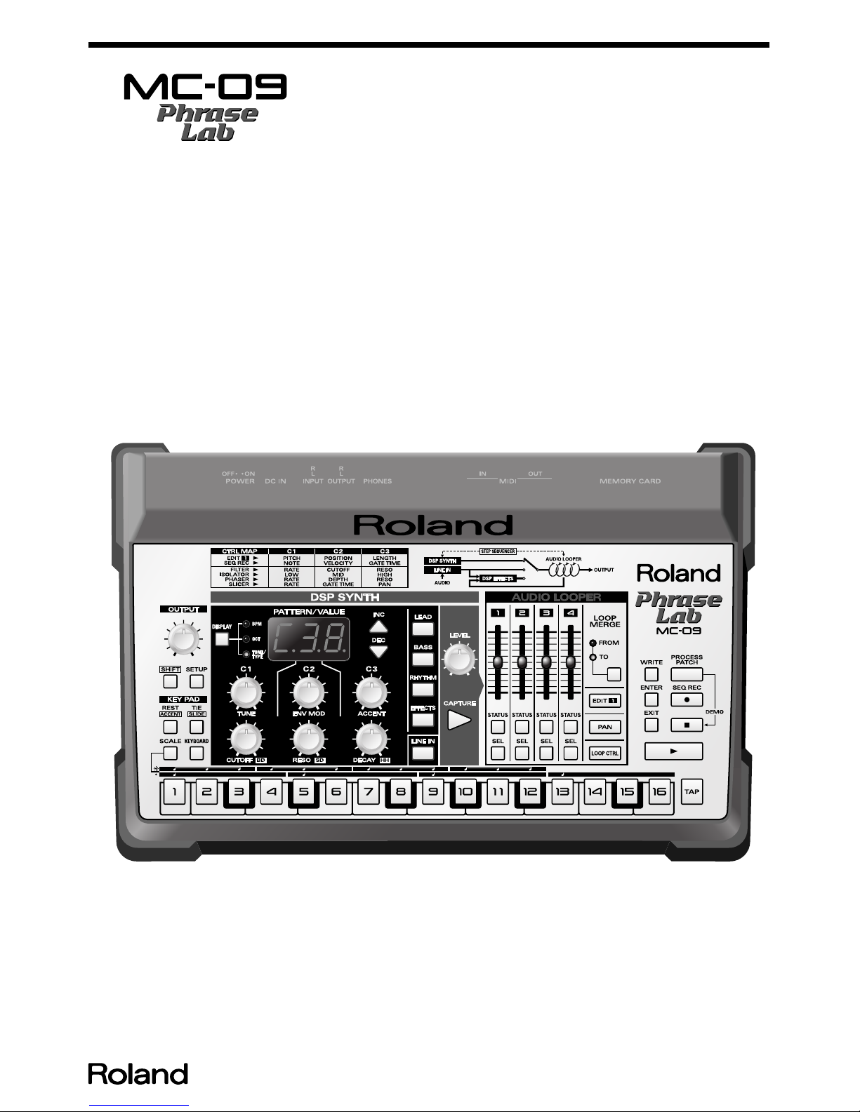
SERVICE NOTES
Issued by RJA
Copyright © 2002 ROLAND CORPORATION
All rights reserved. No part of this publication may be reproduced in any form without the written permission
of ROLAND CORPORATION.
Printed in Japan (
0800
) (AS)17058085EO
May 2002
MC-09
SPECIFICATIONS................................................................. 2
LOCATION OF CONTROLS............................................... 4
LOCATION OF CONTROLS PARTS LIST ....................... 5
EXPLODED VIEW ................................................................ 6
EXPLODED VIEW PARTS LIST ......................................... 7
PARTS LIST............................................................................ 8
CHECKING THE VERSION NUMBER........................... 12
USERS DATA SAVE AND LOAD(MEMORY CARD) .. 12
USERS DATA SAVE AND LOAD(BULK DUMP)......... 12
RESTORING THE FACTORY SETTINGS ....................... 13
SYSTEM SOFTWARE UPDATE PROCEDURE ..............13
TEST MODE.......................................................................... 14
BLOCK DIAGRAM ............................................................. 16
CIRCUIT BOARD(MAIN BOARD 1/2) ...........................18
CIRCUIT BOARD(MAIN BOARD 2/2) ...........................20
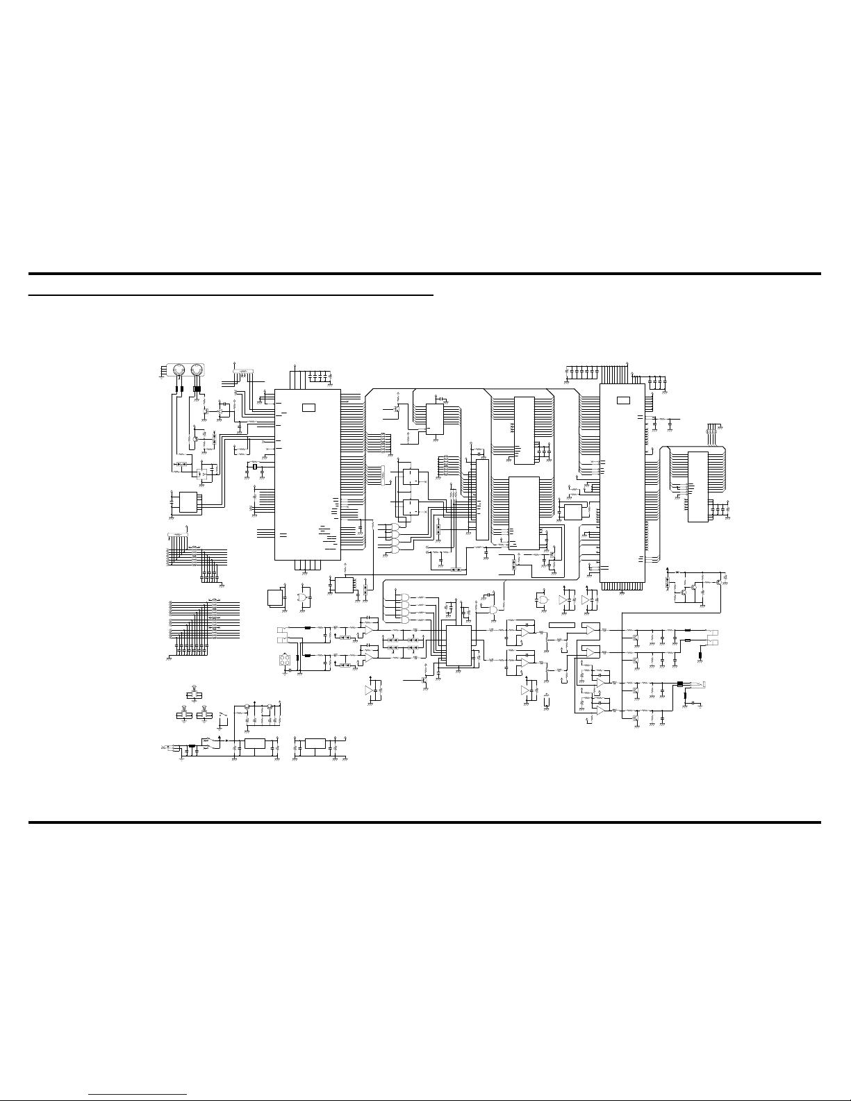
CIRCUIT DIAGRAM(MAIN BOARD 1/2)...................... 22
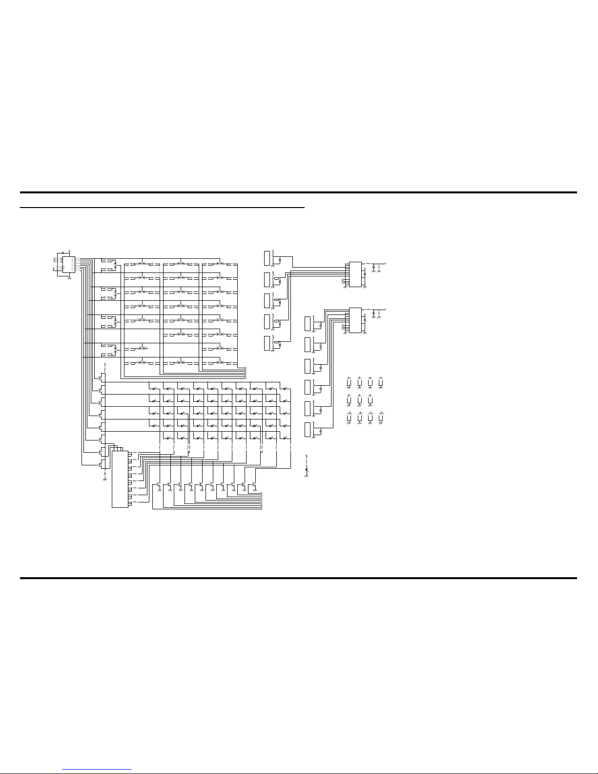
CIRCUIT DIAGRAM(MAIN BOARD 2/2)...................... 24
ERROR MESSAGES............................................................. 26
Page 2

2
May 2002
SPECIFICATIONS
MC-09: Phrase Lab
DSP Synthesizer
Number of Parts
1
Maximum Polyphony
LEAD, BASS: 1
RHYTHM: 3
Preset Tones
LEAD: 128
BASS: 128
RHYTHM: 10
Effects
Type
FILTER, ISOLATOR, PHASER, SLICER
Number of Types
30
LEAD Group
OVERDRIVE, DISTORTION, PHASER, SLICER + RING
MODULATOR
Step Sequencer
Number of Steps
32 (Maximum)
Resolution
sixteenth note
Tempo
quarter note = 40 to 240
Preset Patterns
LEAD: 40
BASS: 60
RHYTHM: 100
EFFECT: 30
User Patterns
LEAD, BASS, RHYTHM, EFFECT: Total 20
External Memory (Memory card)
Pattern, Loop, All: 50 each
Signal Processing
AD Conversion: 24 bits
DA Conversion: 24 bits
Sample Rate
44.1 kHz
Nominal Input Level
INPUT: -10 dBu
Input Impedance
INPUT: 42 k ohm
Nominal Output Level
OUTPUT: -10 dBu
Output Impedance
OUTPUT: 600 ohm
PHONES: 100 ohm
Residual Noise Level
(LINE IN: OFF, input terminated with 150 , IHF-A, typ.)
• 88 dBu
Connectors
INPUT L/R Jacks: RCA phono type
OUTPUT L/R Jacks: RCA phono type
Headphones Jack: Stereo miniature
phone type
MIDI IN/OUT Connectors
DC IN Jack
Ground Terminal
Memory Card Slot
Power Supply
AC Adaptor (DC 9V)
Current Draw
350 mA
Dimensions
318.6 (W) x 207.2 (D) x 69.5 (H) mm
12-9/16 (W) x 8-3/16 (D) x 2-3/4 (H) inches
Weight
1.2 kg / 2 lbs 11 oz (excluding AC Adaptor)
Accessories
Owner’s Manual ENGLISH(#72123212)
JAPANESE(#72123201)
AC Adaptor
·ACI-120C(#00905767)
·ACI-230C(#01018312)
·PSB-1U(#01901578)
LEAD CTRL MAP Seal(#40458390)
Phrase CD (CD-EXTRA format)(#********)
Memory Card Protector(#01346312)
Options
MIDI Implementation ENGLISH(#17041158)
JAPANESE(#17041157)
*0 dBu = 0.775 V rms
* In the interest of product improvement, the specifications and/
or appearance of this unit are subject to change without prior
notice.
Page 3

3
MC-09
Page 4
4
May 2002
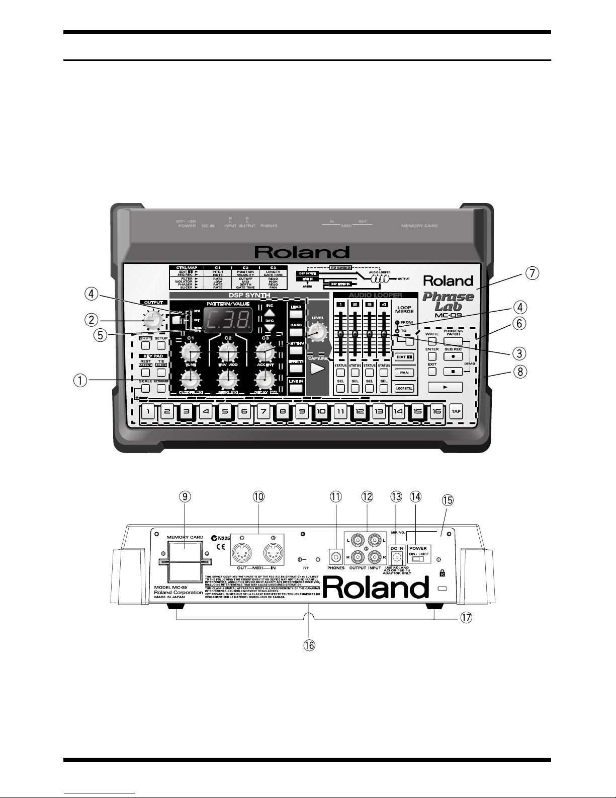
LOCATION OF CONTROLS
fig.top
Page 5

5
MC-09
LOCATION OF CONTROLS PARTS LIST
No
PART CODE Part name Description Q’TY
1 02905734 X R-KNOB MF GLD 7
02455223 EVUF2KFK4B14 9M/M ROTARY POTENTIOMETER 7
2 02905734 X R-KNOB MF GLD 1
02905412 RK12L12C0A0E 12M/M ROTARY POTENTIOMETER 1
3 01346112 KNOB MOLD KNOB BLK 4
02239523 EWAN1AC15B14 30M/M SLIDE POTENTIOMETER 4
4 02126912 PTR LED SLR-342VR-TG7 LED 5
5 01342534 SL-9351S LED 7 SEGMENT 1
6 02905790 RUBBER SW 1
7 02905789 PANEL SHEET 1
8 02905745 TOP CASE 1
9 01343101 D C-ESCT D C-ESCT BX1H BLK 1
02121578 CN015R-3013-0 CARD CONNECTR 1
10 13429676 YKF51-5048 (TWIN) MIDI CONNECTOR 1
11 02456390 STEREO YKB21-5290 3.5MM JACK 1
12 13449645 YKC21-3049 (4P) RED/WHITE JACK (PIN) 1
13 13449720 HEC2305-01-250 DC JACK 1
14 02671312 SLG-22-465 SLIDE SWITCH 1
15 02905767 REAR PANEL 1
16 02905756 BOTTOM COVER 1
17 12359137 RUBBER FOOT SJ-5012 BLK 4
Page 6
6
May 2002
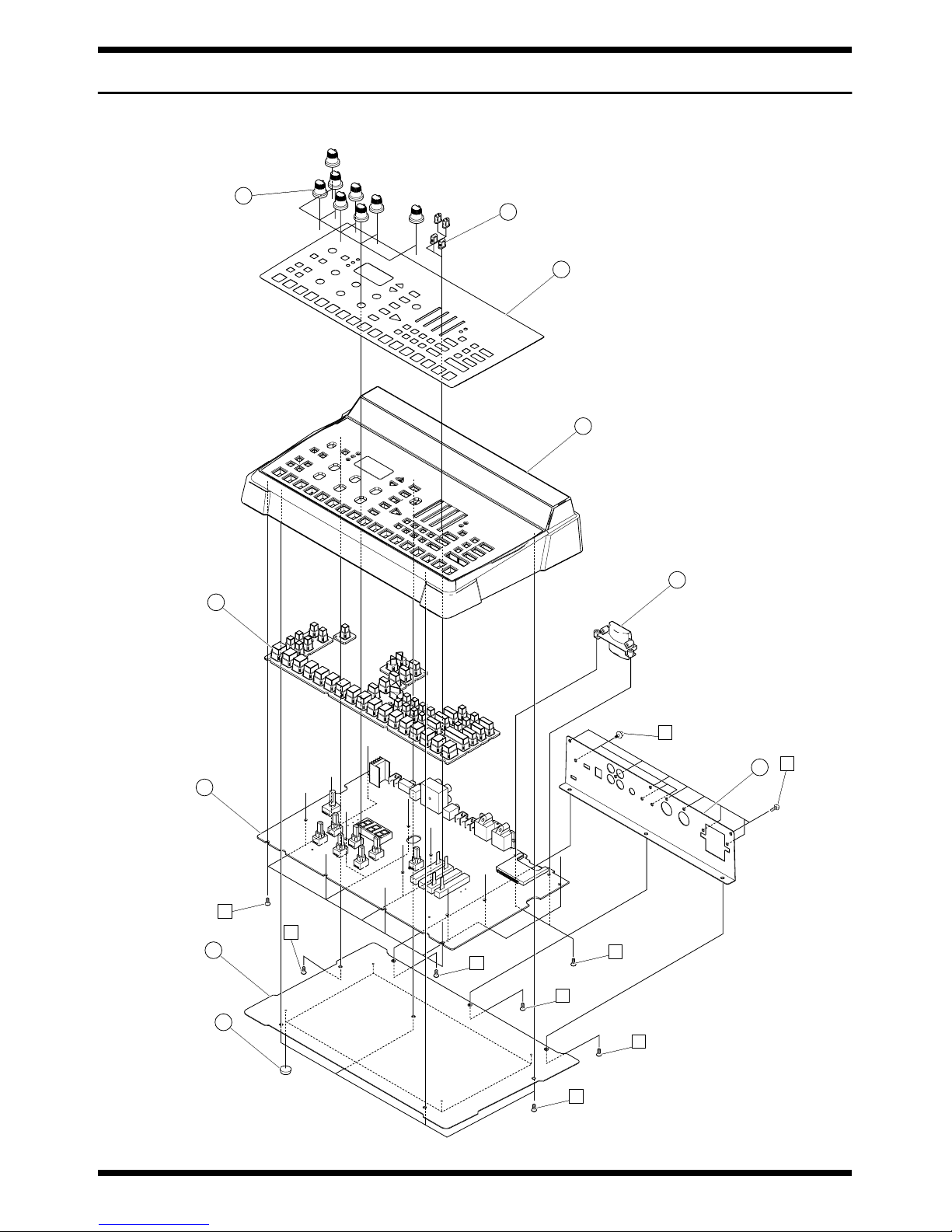
EXPLODED VIEW
fig.explo
1
8
2
9
4
5
6
10
7
a
b
b
c
c
c
c
c
b
3
Page 7

7
MC-09
EXPLODED VIEW PARTS LIST
[PART]
No. PART CODE PART NAME DESCRIPTION
1 02905789 PANEL SHEET
2 02905745 TOP CASE
3 02905767 REAR PANEL
4 02905790 RUBBER SW
4 02905790 RUBBER SW
4 02905790 RUBBER SW
5 72016578 MAIN BOARD ASSY
6 02905756 BOTTOM COVER
7 02905734 X R-KNOB MF GLD
8 01346112 KNOB MOLD KNOB BLK
9 01343101 D C-ESCT D C-ESCT BX1H BLK
10 12359137 RUBBER FOOT SJ-5012 BLK
10 12359137 RUBBER FOOT SJ-5012 BLK
10 12359137 RUBBER FOOT SJ-5012 BLK
10 12359137 RUBBER FOOT SJ-5012 BLK
[SCREW]
No.
PART CODE PART NAME DESCRIPTION
A 40011490 SCREW M3X6 PAN MACHINE W/SW BZC
B 40011090 SCREW 3X6 BINDING TAPTITE B BZC
C 40011301 SCREW M3X6 BINDING P-TITE FE BZC
Page 8
8
May 2002
PARTS LIST
fig.part1e
CASING
#
02905745 TOP CASE 1
# 02905767 REAR PANEL 1
# 02905756 BOTTOM COVER 1
01343101 D C-ESCT D C-ESCT BX1H BLK 1
KNOB, BUTTON
01346112 KNOB MOLD KNOB BLK 4
# 02905734 X R-KNOB MF GLD 8
# 02905790 RUBBER SW 1
SWITCH
02671312
SLG-22-465 SLIDE SWITCH SW1 on Main Board 1
JACK, EXT TERMINAL
13429676
YKF51-5048 (TWIN) MIDI CONNECTOR JK1 on Main Board 1
13449645 YKC21-3049 (4P) RED/WHITE JACK (PIN) JK2 on Main Board 1
02121578 CN015R-3013-0 CARD CONNECTR CN1 on Main Board 1
02456390 STEREO YKB21-5290 3.5MM JACK JK5 on Main Board 1
13449720 HEC2305-01-250 DC JACK JK6 on Main Board 1
DISPLAY UNIT
01342534
SL-9351S LED 7 SEGMENT LED57 on Main Board 1
NOTE: Replacement SL-9351S should be made on a unit base.
PCB ASSY
#
72016578 MAIN BOARD ASSY 1
NOTE: ‘MAIN BOARD ASSY’ includes the following parts.
02014090 HEATSINK K217 H25 1
12199584 GROUNDING TERMINAL M1698 TER3,TER2,TER1 on Main Board 3
40011501 SCREW M3X8
PAN MACHINE W/SW+PW BZC
1
IC
01786667
HD6413006F20 IC (CPU) IC2 on Main Board 1
02231767 RA0A-101 (TC223C080AF-101) IC (DSP) IC1 on Main Board 1
02671378 LC324260BJ-60-TLM IC (DRAM) IC3 on Main Board 1
02450401 GM71C18163CJ-6 IC (DRAM) IC4 on Main Board 1
02232367 HN58X2432FPI IC (EEPROM) IC6 on Main Board 1
********
MBM29F800BA-70PFTN-SFK
IC (FLASH MEMORY)
1
02451434 AK4552VT IC (AD/DA) IC13 on Main Board 1
# 02905445 TC7SET08FU(TE85L) IC (CMOS) IC12 on Main Board 1
15249104 TC7S04F(TE85L) IC (CMOS) IC5 on Main Board 1
02675689 HD74LV245ATELL IC (CMOS) IC33 on Main Board 1
# 02905423 HD74LV4051ATELL IC (CMOS) IC23,IC30 on Main Board 2
01675034 TC74VHC138FT(EL) IC CMOS IC22 on Main Board 1
01679090 TC74VHC08FT(EL) IC (CMOS) IC10 on Main Board 1
01897967 TC74VHC74FT(EL) IC (CMOS) IC27 on Main Board 1
01899156 TC74VHC32FT(EL) IC (CMOS) IC32 on Main Board 1
15189261 M5218AFP-600E IC (BIPOLAR OP AMP) IC17,IC16,IC15,IC11 on Main Board 4
01458445 UPC29M33T-T1 IC (REGULATOR) IC21 on Main Board 1
02014645 BA17805T IC (REGULATOR) IC19 on Main Board 1
15289123 M51953AFP-600C IC (RESET) IC9 on Main Board 1
02900545 PC410LKNIP IC (PHOTO COUPLER) IC7 on Main Board 1
TRANSISTOR
01784790
2SA1602A-T11-1F TRANSISTOR Q4,Q2 on Main Board 2
SAFETY PRECAUTIONS:
The parts marked have
safety-related characteristics. Use
only listed parts for replacement.
CONSIDERATION ON PARTS ORDRING
When ordering any parts listed in the parts list, please specify the following items in the order sheet.
QTY PART NUMBER DESCRIPTION MODEL NUMBER
Ex.10 22575241 Sharp Key C-20/50
15 2247017300 Knob (orange) DAC-15D
Failure to completely fill the above items with correct number and description will result in delayed or even
undelivered replacement.
NOTE: The parts marked # are new. (initial parts)
Page 9

9
MC-09
15319102
2SC2882-Y(TE12L.C) TRANSISTOR Q11 on Main Board 1
15319116 2SC4154-T11-F TRANSISTOR Q34,Q6,Q5 on Main Board 3
02670989 DTB113ZK-146T TRANSISTOR Q17,Q16,Q18,Q19,Q20,Q21,Q22,Q15 on
Main Board
8
# 02905856 UNR5211-(TX) TRANSISTOR Q29,Q30,Q32,Q35,Q33,Q1,Q28,Q27,Q26,Q2
5,Q24,Q23,Q31 on Main Board
13
15329536 RN1442-A(TE85L) TRANSISTOR Q8,Q7 on Main Board 2
DIODE
15339412
U1BC44(TE12L) DIODE D1 on Main Board 1
02014778 U1GC44(TE12L) RECTIFIER DIODE D2 on Main Board 1
15339130 MA142WK-(TX) ARRAY DIODE DA33,DA22,DA23,DA25,DA30,DA20,DA32
,DA24,DA34,DA36,DA37,DA38,DA31,DA1
8,DA17,DA16,DA15,DA13,DA12,DA11,DA
3,DA2,DA1,DA19,DA27 on Main Board
25
01897178 MA142WA-(TX) ARRAY DIODE DA46,DA51,DA29,DA47,DA48 on Main
Board
5
01897189 MA147-(TX) ARRAY DIODE DA54,DA6,DA5,DA7,DA41,DA8,DA40,DA
53 on Main Board
8
02671245 SML-310LTT86 LED LED20,LED33,LED16,LED17,LED19,LED21
,LED22,LED23,LED26,LED27,LED28,LED2
9,
44
LED30,LED15,LED32,LED39,LED36,LED37
,LED40,LED42,LED43,LED45,LED46,LED4
7,LED58,LED59,LED60,LED1,LED18,LED3
1,LED8,LED41,LED14,LED3,LED4,LED5,L
ED6,LED7,LED2,LED9,LED10,LED13,LED1
1,LED12 on Main Board
02126912 SLR-342VR-TG7 LED LED34,LED48,LED24,LED38,LED44 on
Main Board
5
RESISTOR
15399565
RPC18T 470 J CARBON RESISTOR R55,R72,R56,R71 on Main Board 4
01011856 RPC05T 0R0 J MTL.FILM RESIST0R R149,R125,R150,R147,R179,R148,R43 on
Main Board
7
00567378 RPC05T 473 J MTL.FILM RESISTOR R27,R28,R40,R48,R49,R50,R64,R65 on Main
Board
8
00567501 RPC05T 474 J MTL.FILM RESISTOR R53,R157,R34,R41,R156,R63 on Main Board 6
00567412 RPC05T 104 J MTL.FILM RESISTOR R58,R175,R165,R75,R122 on Main Board 5
00567289 RPC05T 103 J MTL.FILM RESISTOR R10,R176,R8,R152,R68,R174,R69,R77,R80,R
173,R170,R153,R2 on Main Board
13
00567434 RPC05T 154 J MTL.FILM RESISTOR R25 on Main Board 1
00567234 RPC05T 392 J MTL.FILM RESISTOR R51,R66 on Main Board 2
00567089 RPC05T 331 J MTL.FILM RESISTOR R163,R162,R78,R31,R6,R4 on Main Board 6
00566967 RPC05T 470 J MTL.FILM RESISTOR R13 on Main Board 1
00567034 RPC05T 121 J MTL.FILM RESISTOR R12 on Main Board 1
00567067 RPC05T 221 J MTL.FILM RESISTOR R109,R7,R1 on Main Board 3
00567112 RPC05T 471 J MTL.FILM RESISTOR R46,R30,R38,R59,R32 on Main Board 5
00567190 RPC05T 222 J MTL.FILM RESISTOR R11,R29 on Main Board 2
00567245 RPC05T 472 J MTL.FILM RESISTOR R26,R5 on Main Board 2
00567023 RPC05T 101 J MTL.FILM RESISTOR R137,R182,R181,R167,R166,R164,R159,R144,
R143,R142,R141,R140,R138,R9,R121,R119,R
118,R117,R116,R115,R114,R113,R112,R111,R
110,R39,R33,R3,R139 on Main Board
29
00567278 RPC05T 822 J MTL.FILM RESISTOR R67,R52 on Main Board 2
00567301 RPC05T 153 J MTL.FILM RESISTOR R79 on Main Board 1
00567323 RPC05T 223 J MTL.FILM RESISTOR R61,R45 on Main Board 2
00903956 MCR100 JZH J 4R7 MTL.FILM RESISTOR R120 on Main Board 1
15399965
RCE9A103JAG7A (10KOHM X8)
RESISTOR ARRAY RA18,RA9,RA10 on Main Board 3
01906678 MNR14 EOAB J 103 RESISTOR-ARRY RA6,RA25,RA17,RA24 on Main Board 4
01906945 MNR14 E0AB J 101 RESISTOR-ARRY RA16,RA15,RA13,RA14 on Main Board 4
02239645 MNR14 E0AB J 102 RESISTOR-ARRAY RA11,RA12 on Main Board 2
POTENTIOMETER
02455223
EVUF2KFK4B14
9M/M ROTARY POTENTIOMETER
VR6,VR13,VR11,VR5,VR4,VR3,VR12 on
Main Board
7
# 02905412 RK12L12C0A0E
12M/M ROTARY POTENTIOMETER
VR2 on Main Board 1
02239523 EWAN1AC15B14
30M/M SLIDE POTENTIOMETER
VR8,VR7,VR10,VR9 on Main Board
4
CAPACITOR
01674334
ECUV1H101JCV CERAMIC CAPACITOR C48,C16,C33,C44,C45,C47,C49,C50,C58,C59
,C60,C61,C63,C191,C192,C46,C62 on Main
Board
17
02129534 ECJ1VB1H102K CERAMIC CAPACITOR C17,C31 on Main Board 2
01674190 ECUV1H150JCV CERAMIC CAPACITOR C28,C29 on Main Board 2
01674389 ECUV1H221JCV CERAMIC CAPACITOR C96,C111,C104,C91,C77,C70 on Main Board 6
01674612 ECJ1VB1H103K CERAMIC CAPACITOR C185,C65,C54,C53,C66,C67,C51,C157,C52
on Main Board
9
TRANSISTOR
Page 10
10
May 2002
01674701
ECJ1VF1E104Z 0.1UF/16VK CERAMIC CAPACITOR(CHIP) C178,C138,C139,C141,C144,C145,C151,C19
0,C158,C41,C179,C180,C186,C132,C154,C10
,C81,C107,C9,C11,C15,C18,C27,C102,C37,C
39,C75,C82,C99,C32,C8,C106 on Main
Board
32
01674712 ECJ1VF1A105Z CERAMIC CAPACITOR C5,C4,C3,C2,C24,C22,C6,C167,C25,C12,C13
,C20,C21,C26,C40,C131,C169,C170,C130 on
Main Board
19
# 01346889 ECHU1H151JX5 POLYEST. CAPACITOR C103,C86 on Main Board 2
01784145 ECHU1H152JX5 POLYEST. CAPACITOR C92,C108 on Main Board 2
13639546M0 ECEA1CKA100B 10UF/16V CHEMICAL CAPACITOR C133,C88,C87,C89,C90,C173,C172,C171,C14
0,C109,C105,C100,C98,C97,C94,C142,C30,C
80,C42,C74,C83,C93 on Main Board
22
13639547M0 ECEA1CKA220B 22UF/16V CHEMICAL CAPACITOR C19,C38,C153 on Main Board 3
13639550M0 ECEA1CKA101B 100UF/16V CHEMICAL CAPACITOR C155,C115,C112 on Main Board 3
13639549M0 ECEA1CKA470B CHEMICAL CAPACITOR C23,C113,C150 on Main Board 3
01902612 RA2-6V471MC-T2 CHEMICAL CAPACITOR C146 on Main Board 1
02014890 RA2-16V221MT2 CERAMIC CAPACITOR C36,C116 on Main Board 2
02239623 RA2-16V102M-T2 CHEMICAL CAPACITOR C143 on Main Board 1
CAPACITOR
INDUCTOR, COIL, FILTER
01565612
DSS310-93D223S50 EMI FILTER FL1 on Main Board 1
01565589 N1608ZA601T01 FERRITE-BEAD L8,L2,L3,L5,L15,L9,L10,L11,L12,L13,L14,L1
6,L1,L4 on Main Board
14
CRYSTAL, RESONATOR
00894023
MA-406 20.000MHZ TE24 CRYSTAL X1 on Main Board 1
01893334 SG8002JC-67.7376M-PHCL OSCILLATOR X2 on Main Board 1
SCREW
40011090
SCREW 3X6 BINDING TAPTITE B BZC 3
40011301 SCREW M3X6 BINDING P-TITE FE BZC 29
40011490 SCREW M3X6 PAN MACHINE W/SW BZC 3
PACKING
#
02905690 LOWER PAD 1
# 02905701 UPPER PAD 1
# 02905689 PACKING CASE 1
# 02905834 OUTER PACKING CASE 1
# 40458989 RECYCLE MARK SEAL FOR PACKING 1
MISCELLANEOUS
40237123
NITTO DAMPLON K60 #3505 W50MM 50M 140
12359137 RUBBER FOOT SJ-5012 BLK 4
# 02905789 PANEL SHEET 1
ACCESSORIES (STANDARD)
00905756 AC ADAPTOR ACI-100C 1
00905767 AC ADAPTOR ACI-120C 1
01018312 AC ADAPTOR ACI-230C 1
01901578
AC ADAPTOR WITHOUT AC CORD
PSB-1U UNIVERSAL
1
01903356 AC CORD SET 230V 1.0M FOR PSB 1
01903367 AC CORD SET 240V 1.0M FOR PSB 1
00905234 EURO CONVERTER PLUG
ECP01-5A (PLUG FOR BRC-230T)
1
# 72123201 OWNER’S MANUAL SET JAPANESE 1
# 72123212 OWNER’S MANUAL SET ENGLISH 1
# ******** PHRASE CD 1
# 40458390 LEAD CTRL MAP SEAL 1
01346312 CARD PROTECTOR 1
40232334 WARRANTY CARD MOCHIKOMI JAPAN ONLY 1
Page 11

11
MC-09
Page 12

12
May 2002
CHECKING THE VERSION
NUMBER
1.
Turn off the main power.
2.
While holding down [SHIFT] and STEP [4], turn on the main power.
3.
The version number of the software will appear on the display and the
test mode will be turned on .
4.
The mode will end when the main power is turned off.
USERS DATA SAVE AND
LOAD(MEMORY CARD)
Memory cards usable with the
MC-09
The MC-09 can use commercially available SmartMedia
memory cards. However, a memory card is not included.
You can purchase a memory card at a nearby computer shop
or digital camera dealer. When you purchase a memory card,
make sure that it meets the following conditions.
· Power supply voltage: 3.3 V
· Capacity: 2 MB-128 MB
* The MC-09 cannot use SmartMedia of types other than the above.
* If you use 2 MB Smart Media, it may not be possible to save all data.
Cautions when using a memory
card
* The power of the MC-09 must be off when you insert or remove a memory card.
Inserting or removing a memory card when the power is on will damage the
memory card as well as the data in the MC-09.
* Make sure that the memory card is oriented correctly (The surface without gold
contactsmust face upward), and push it all the way into the slot.
* Never turn on the power when a memory card is inserted part-way into the slot.
Doing so will damage the data in internal memory.
* Never turn off the power while ”BSY” appears in the display. Doing so will
damage the data in the memory card and internal memory.
Formatting a memory card
This operation prepares the memory card for use on the MC-09.
You will need to format a newly purchased memory card
before using it for the first time, or before a memory card
used with another device can be used on the MC-09.
* When you format a memory card, the entire contents of the card will be erased.
1.
Press the [SETUP] button.
2.
Press the [INC] or [DEC] button until the display indicates "FMT”.
3.
Press the [ENTER] button. The display will show "SUR”.
4.
To format the card, press the [WRITE] button. While the card is being
formatted, "BSY” will appear in the display. When formatting is finished,
you’re returned to where you were in step 2.
* If you decide not to format the card, press the [SETUP] button or the [EXIT]
button.
5.
Press the [SETUP] button.
Saving all settings of the MC-09
to a memory card
The following settings stored in the audio looper will be
saved together on the memory card.
· All loops and user patterns
· Process patch
· System settings
· The settings of the currently selected pattern/effect pattern
For details on system settings, refer to "Parameter list”
1.
Press the [SETUP] button.
2.
Press the [INC] or [DEC] button until the display indicates " AL.L”.
3.
Press the [ENTER] button. The display will show the save-destination file
number (A01- A50).
4.
Use the [INC] and [DEC] buttons to select the desired save-destination
file number.
* Should you decide that you don’t want to carry out the save, press the [SETUP]
button or the [EXIT] button.
5.
Press the [WRITE] button to begin saving. While the settings are being
saved, the display will show "BSY”. Once the save is complete, you’re
returned to where you were in step 2.
* If the save-destination file number already exists on the memory card, the display
will indicate "SUR”. If you want to save the new data by overwriting the old,
press the [ENTER] button. If you want to save the data with a different file
number, press the [EXIT] button and repeat the procedure from step 2.
* It may take up to three minutes for saving one loop.
6.
Press the [SETUP] button. When loops are saved to a memory card, they
are saved in the MC-09’s own original format.
Loading MC-09 settings
Here's how MC-09 settings saved on a memory card can be
loaded back into the MC-09.
1.
Press the [SETUP] button.
2.
Press the [INC] or [DEC] button until the display indicates "AL.L".
3.
Press the [ENTER] button. The display will show one of the file numbers
(A01-A50) that have been saved in the memory card.
4.
Use the [INC] and [DEC] buttons to select the file number that you want
to load.
* If you decide not to load a file, press the [SETUP] button or the [EXIT] button.
5.
Press the [WRITE] button. The display will indicate "SUR”, asking you to
confirm the operation.
6.
Press the [ENTER] button to load MC-09 settings. While the settings are
being loaded, the display will show "BSY”. Once the data's been loaded,
you’re returned to where you were in step 2.
* It may take up to three minutes for loading one loop.
7.
Press the [SETUP] button.
USERS DATA SAVE AND
LOAD(BULK DUMP)
Saving the MC-09 settings to an
external sequencer (Bulk Dump)
Data for the currently selected pattern, process patch or all saved settings, can
be transmitted to an external MIDI device. This function is called bulk dump.
You can create a backup of the MC-09's data by using bulk dump to record the
data on an external MIDI sequencer. You can also use this function to replicate
the current settings of one MC-09 (except for the Loop setting) on another MC-
09.
Page 13

13
MC-09
Saving MC-09 data on an
external MIDI sequencer
1.
Use a MIDI cable to connect the MC-09’s MIDI OUT tothe MIDI IN of
your external MIDI sequencer.
2. Press the [SETUP] button.
3. Press the [INC] or [DEC] button until the display indicates "DMP”(Bulk
Dump).
4. Press the [ENTER] button.
5. Use the [INC] and [DEC] buttons to select the data that you want to
save.Ptn: Settings for the currently selected pattern Ptc: Process
patchesALL: All patterns, process patches, and system settings
6. Press the [ENTER] button. The display will blink "SUR”(Sure), asking you
to confirm the operation. If you decide to cancel, press the [EXIT] button.
7. Begin recording on your external MIDI sequencer.
8. Press the [ENTER] button to initiate the bulk dump. While the data is
being transmitted, the indication in the display will blink. When
transmission is completed, the display will show “END”.
9. Stop recording on your external MIDI sequencer.
10. Press the [EXIT] button to complete the bulk dump.
Restoring MC-09 data from an
external MIDI sequencer
The data that was saved by a bulk dump is referred to as bulk data. By loading
this bulk data, you can reproduce the state in which the MC-09 was when it
transmitted the bulk data.
1. Use a MIDI cable to connect the MC-09’s MIDI IN to the MIDI OUT of the
external MIDI sequencer.
2. Press the [SETUP] button.
3. Press the [INC] or [DEC] button until the display indicates "rcv”(Bulk
Receive).
4. Press the [ENTER] button. The MC-09 will wait to receive bulk data. If
you decide to cancel, press the [EXIT] button.
5. Play back your external MIDI sequencer to transmit the bulk data to the
MC-09. While the MC-09 is receiving bulk data, the display will
blink.When bulk data reception ends, the display will indicate “BSY”.
This display will continue for approximately 60 seconds.
* Never turn off the power while "BSY”appears in the display. Doing so will
damage the data in the memory card and internal memory.
* You must transmit all of the bulk data.
6. Press the [EXIT] button to complete the operation, after the display
indicates “rcv”.
RESTORING THE FACTORY
SETTINGS
Restoring the factory settings
(Factory Reset)
By carrying out a Factory Reset, the following settings of the MC-09 are
restored to their original factory-set condition.
· System settings
· All patterns you’ve saved (User Patterns)
* Once you execute a Factory Reset, all the settings you’ve saved will be lost, being
replaced by the settings your unit originally had when it left the factory. If
internal memory contains important data that you want to keep, you must save
it on a memory card, or to an external MIDI sequencer via bulk dump.
1. Press the [SETUP] button.
2. Press the [INC] or [DEC] button until the display indicates “Fct”.
3. Press the [ENTER] button. The display will show “Sur”.
4. To execute the factory reset, press the [WRITE] button. While the factory
settings are being restored, “BSY” will appear in the display. When the
factory reset is finished, you’re returned to where you were in step 2.
* If you decide not to restore the factory settings, press the [SETUP] button or the
[EXIT] button.
* Never turn off the power while “BSY”appears in the display. Doing so will
damage the system.
5. Press the [SETUP] button to return to the previous display.
SYSTEM SOFTWARE UPDATE
PROCEDURE
General Outline
The MC-09 uses a Flash Memory for the system program.
The Flash Memory updater (control program) is stored within the Flash
Memory.
Generally, data for updating is provided in divided SMF data. The program
version is updated by connecting a playable sequencer (MC-80, etc.) to the MC-
09 with a MIDI cable and then loading SMF data to the MC-09.
The Flash Memory consists of 2 areas and modes: FIX (with updating and test
mode programs) and USER (with main program) areas, and ALL (for both FIX
and USER areas) and USER (for USER area only) updating modes.
Updating is only available via MIDI.
Note:
If updating fails in ALL updating mode, the unit may become permanently
unrebootable. In this case, the current Flash Memory must be replaced with the
one already written in with program.
After updating, factory reset is necessary. Back up the user data in advance
since it will be reset. Details are described in “Saving and loading data”.
Device Used in Updating Mode
MC-09 and AC adapter
Sequencer that can playback SMF (MC-80, etc.)
MIDI cable x 1
SMF data disk for updating (2HD) x 1 (#17041155)
Files on SMF disk are as follows:
File names remain the same even after version updating.
Update Disk
UP_U_TKO.MID
UP_A_TKO.MID
_TKO00.MID
_TKO01.MID
_TKO02.MID
_TKO03.MID
_TKO04.MID
_TKO05.MID
_TKO06.MID
_TKO07.MID
_TKO08.MID
_TKO09.MID
_TKO10.MID
_TKO11.MID
Common Updating Procedure in
ALL and USER Updating Modes
1. Connect the power code to the respective devices to be used and confirm
that the power can be turned on.
2. Confirm the MC-09’s version prior to updating if necessary.
Page 14

14
May 2002
3. Connect MIDI OUT of the sequencer and MIDI IN of the MC-09 with the
MIDI cable.
Beyond these steps, proceed according to the updating mode.
Procedure for ALL Updating
Mode
1. While holding down the [SEL] buttons of parts 1, 2 and 4 of AUDIO
LOOPER, “ALL” appears on the display when the power is turned on.
2. Load the SMF data [UP_A_TKO.MID] from the sequencer.
3. “Ers” appears on the display and the Flash Memory is
initialized.Approximately 10 seconds later, “UPd” appears on the
display.(Do not load the data while “Ers” is displayed.)4. Load the SMF
data for updating from the sequencer.Playback the 12 [_TKO00.MID] [_TKO11.MID] files in numerical order.
4. While loading the data, the LED of the [START] button blinks and the
number displayed is incremented.
5. When all files have been loaded, “End” appears on the display to indicate
completion of updating. Approximately 10 minutes is required for
loading all of the SMF files.
6. After completion of updating, turn on the main power again, enter the
test mode, confirm the version and conduct a device check. Subsequently,
conduct factory reset.
Procedure for USER Update Mode
1. While holding down the [SEL] buttons of parts 1, 3 and 4 of AUDIO
LOOPER, “USR” appears on the display when the power is turned on.
2. Load the SMF data [UP_U_TKO.MID] from the sequencer.
3. “Ers” appears on the display and the Flash Memory is
initialized.Approximately 10 seconds later, “UPd” appears on the
display.(Do not load the data while “Ers” is displayed.)
4. Load the SMF data for updating from the sequencer. Playback the 11
[_TKO01.MID] - [_TKO11.MID] files in numerical order.
5. While loading the data, the LED of the [START] button blinks and the
number displayed is incremented.
6. When all files have been loaded, “End” appears on the display to indicate
completion of updating.
7. After completion of updating, turn on the main power again, enter the
test mode, confirm the version and conduct a device check. Subsequently,
conduct factory reset.
Actions to be Taken when the
Unit became Unrebootable
Turning off the power accidentally while update may cause improper booting
of the unit.
1. Replace the board if booting becomes impossible after ALL update.
2. Repeat the USER updating procedure again if the unit becomes
unrebootable after USER update.
List of Error Messages Displayed
upon Updating
Er0:Erase Error
Displayed when contents of the Flash Memory cannot be initialized. It is
assumed that the power is not supplied to the VPP terminal of the Flash
Memory.
Er1:Write Error
Displayed when an error occurs while trying to write the Flash Memory.
Er2:Message Error
Displayed when a problem exists in received MIDI message. (SumCheck, etc.)
Er3:FIFO Over Flow
Displayed when the MC-09 cannot process a large amount of MIDI messages
received all at once.
Er4:Overrun Error
Displayed when a MIDI message is missed.
Er5: Framing Error
Displayed when a problem exists in the received MIDI message data such as
transfer rate and jitter.
Er6:Compare Error
Displayed when a difference is found upon comparison of data written in the
Flash Memory and data to be written to the Flash Memory.
TEST MODE
Devices to be Used
MIDI cable x 1
Oscillator
Noise meter
Oscilloscope
Audio cable
Smart Media Card
Method of Booting in the Test
Mode
While holding down [SHIFT] and Step [4], turn on the main power.
Automatically proceeds to version display of item 1.
* Selection of Test Items Proceed through the items in the test mode by holding
down [SETUP] and [TAP]. Moreover, holding down [SETUP] and Step [Item
Number] proceeds directly to the desired inspection item.
Details on Each Test Item
1:Version Display
Displays the program version on the display.
Ex: “1.03” appears on the display when the version is 1.03.
* Holding down [SETUP] and [TAP] proceeds to the next item.
2:Device Test
Performs an operation check on each device (IC).
Insert the Smart Media Card (voltage: 3.3V, capacity: 2-128MB) into the
memory card slot beforehand.
“DEV” appears on the display and checking in the following order
automatically starts:
Step [4] will light if ESP RAM (IC1) is O.K.
Step [2] will light if WORK RAM (IC3) is O.K.
Step [3] will light if EEP RAM (IC6) is O.K.
Step [5] will light if Smart Card is O.K.
Step [1] will light if Flash ROM (IC8) is O.K.
Requires approximately one minute to complete.
“ok” appears on the display when all are confirmed to be O.K.
If an error occurs, the error number appears on the display and procession to
the next item is disabled.
Page 15

15
MC-09
* Holding down [SETUP] and [TAP] proceeds to the next item.
3: MIDI Test
Confirm open and short statuses of MIDI IN and OUT.
Connect 1 MIDI cable to MIDI IN/OUT connector to form a loop beforehand.
“000” indicating short status is displayed.
Remove the MIDI cable connection.
* If the MIDI cable is not connected beforehand, “---” indicating open status is
displayed.In this case, connect 1 MIDI cable to MIDI IN/OUT connector to form
a loop.When confirmed to be O.K., it will automatically proceed to the next item.
4: SW/ LED Test
Checking the LED and SW operations.
Initially, all LEDs corresponding to all the switches will light. Confirm that all
LEDs are lit. Pressing each SW turns off the corresponding LED.
If the SW has an LED, the LED will go out. For SWs without LEDs, the LEDs
will correspond to the SWs as shown in the chart below.
* There is no reaction when 2 or more SWs are held down. Pressing all SWs and
turning off all LEDs will automatically proceed to the next item.
5: VR test
Confirm whether or not the volume functions properly.
Initially, “Vr” appears on the display.Rotating each volume control will
display volume value “000”-”127” for whichever one is currently being
operated.
All LEDs will blink when minimum “000” and maximum “127” values for each
volume are properly obtained.
Completing all volume checks will automatically proceed to the next item.
* Output volume is not included in this test.
6: BYPASS Test
Checks for residual noise and whether or not the signal input from INPUT is
properly output from OUTPUT. “BPS” appears on the display.
6-1: Confirmation of Residual Noise Rotate the OUTPUT volume control to its
maximum position.
Check the residual noise of the output signal from the rear OUTPUT jack with
the noise meter.
The residual noise level is as follows.
• 75 dBm or lower (JIS-A) 6-2:Confirming Output Signal Input oscillator
signal to the rear INPUT jack.
Input signal: 100Hz/ 1kHz/ 10kHz: +6dBm sinewave
Rotate the OUTPUT volume control to its maximum position.
Measure the level of the output signal from the rear OUTPUT jack with the
noise meter.
Confirm that the output signal level for each input signal is within the range of
+4dBm - +8dBm.
For 1kHz sinewaves only, check for distortions in wave form with the
oscilloscope.
* Holding down [SETUP] and [TAP] proceeds to the next item.
7: Initialize
Reset the user memory built into the main unit to factory shipment setting.
After “ini” appears for a few seconds on the display, “Sur” appears and blinks.
Press the [Enter] button to execute.
“BSY” appears on the display during execution.
Requires approximately one minute to complete.
“ini” reappears on the display when initialization is completed.
* ”End” appears on the display when [SETUP] and [TAP] are held down and
switching to normal mode is done automatically.
Error number and error content
ER1 Checksum error in Flash ROM.
ER2 Access error in Work RAM.
ER3 Access error in EEP ROM.
ER4 Access error in ESP RAM.
ER5 Access error in Smart Media.
SWs without LEDs Corresponding to LEDs
[DISPLAY] button [BPM]
[INC] button [OCT]
[DEC] button [TONE/TYPE]
[TAP] button “8” of right part of 7-segment dis-
play
[SHIFT] button “8” of left part of 7-segment display
[ENTER] button [FROM]
[EXIT] button [TO]
[STOP] button Beat LED (located close to the Mem-
ory Card connector)
Page 16
17
May 2002 MC-09
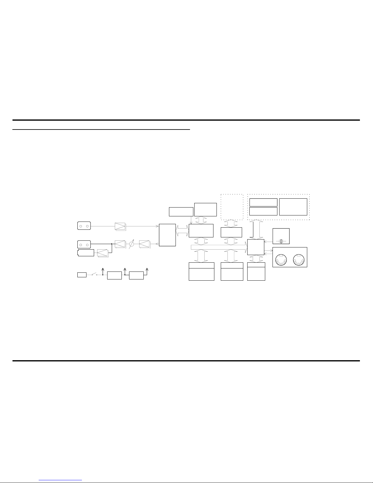
BLOCK DIAGRAM
fig.block
SW1
(256k x 16bit)
IC2
JK6
X'TAL
(32kbit)
Rotary Volume
Power Switch
TC223C080AF
Flash ROM
IC3
CPU
+5V
Switch Matrix
LED Matrix
IC1
X1
IC13
IC8
DRAM
OUTPUT
WORK RAM
+9V
JK2A
OUTPUT
PROGRAM ROM
24bit
(512k x 16bit)
signal processor
JK1
Slide Fader
MBM29F800BA-70PFTN
&
DC9V IN
IC6
ADA
LC324260AJ-60
H8/3006
IC19
OUT
2ch codec
+5V
REGULATOR
JK5
user memory
IN
MIDI
IC15
HN58X2432FP
AK4552AF
PHONES
ESP4
EEPROM
IC11,14,15,16,17 OP.AMP,M5218
20.000MHz
OUTPUT
REGULATOR
+3.3V
IC21
+3.3V
IC16
IC17
IC11
INPUT
JK2B
LINE
X2
67.7376MHz
OSCILLATOR
IC33
HD74LV245ATELL
bus transceiver
GM71C18163CJ-6
DRAM
(1024k x 16bit)
IC4
Smart Media
CN1
LINE
Page 17
19
May 2002 MC-09
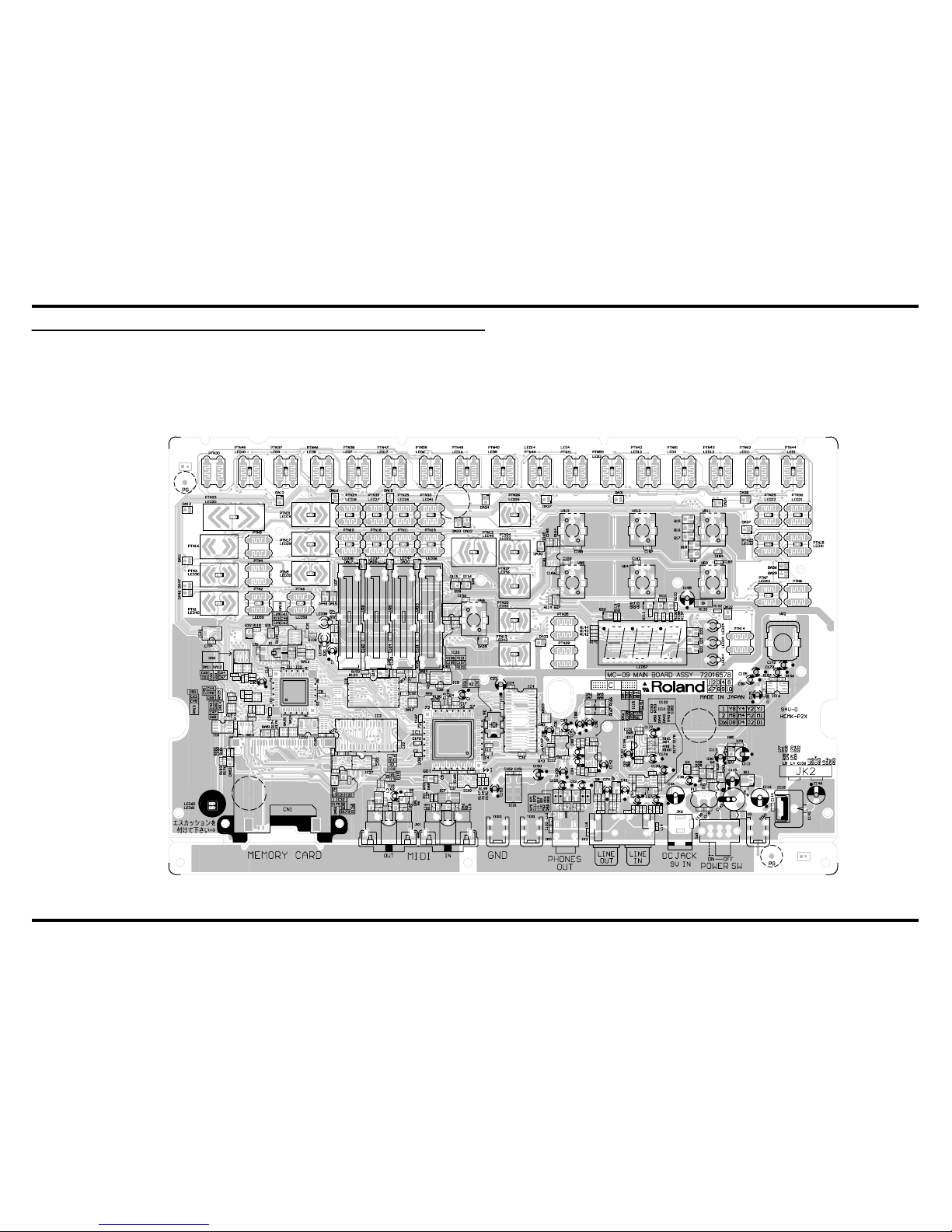
CIRCUIT BOARD(MAIN BOARD 1/2)
fig.block
View from component side
Page 18
21
May 2002 MC-09
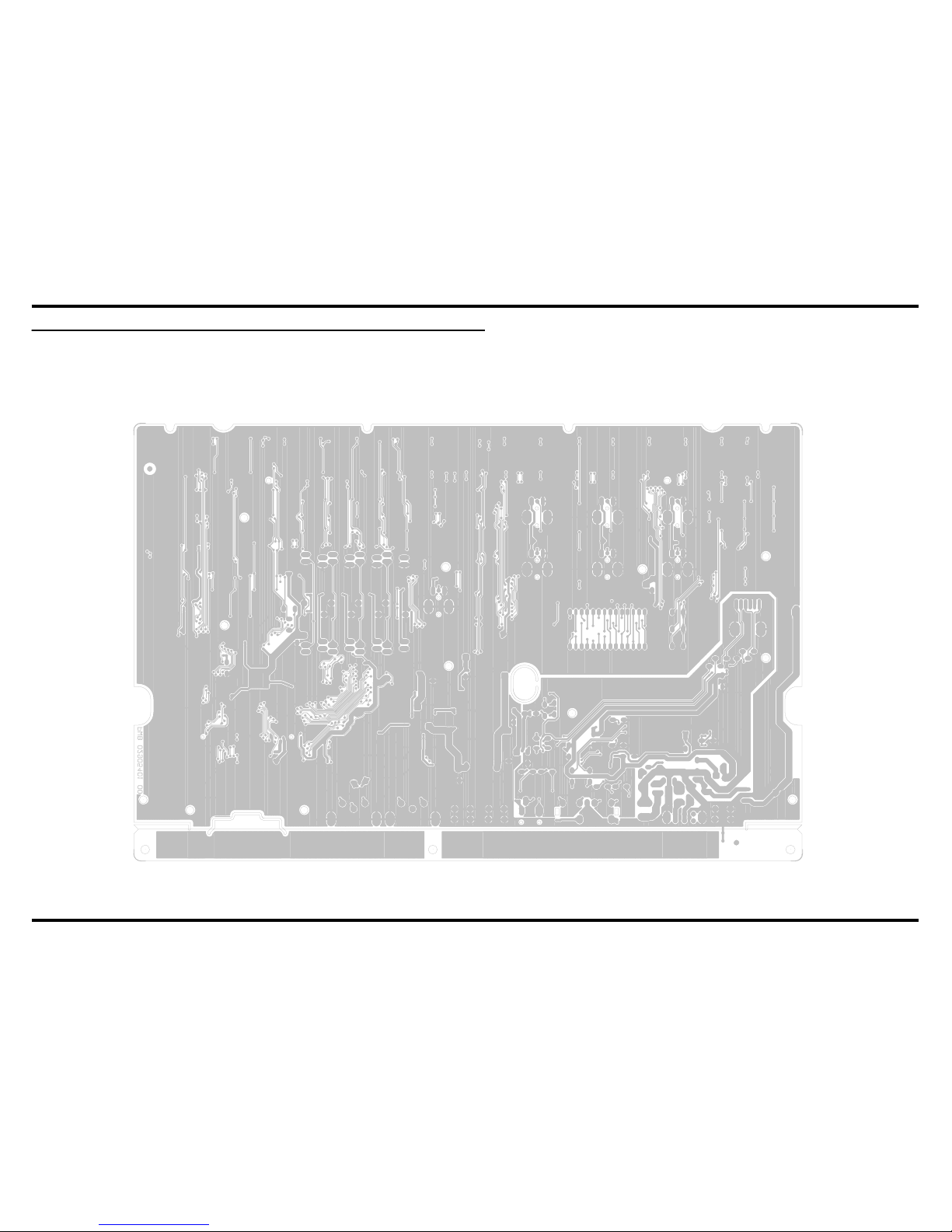
CIRCUIT BOARD(MAIN BOARD 2/2)
fig.block
View from foil side
Page 19
23
May 2002 MC-09
CIRCUIT DIAGRAM(MAIN BOARD 1/2)
fig.main1
From
ADAPTOR
DSP
DSPDSP
DSP
*64Fs
*256Fs
IN/OUT
MIDI
(100mA)
MAX
(170mA)
MAX
MAX
(3mA)
(150mA)
MAX
R
+6dB
+6dB+6dB
+6dB
[-24dBu]
[-24dBu][-24dBu]
[-24dBu]
L
Q:0.8
(20mA)
-10dBu
CUT OFF:25kHz
INPUT
+14dB
+14dB+14dB
+14dB
OUTPUT
(45mA)
MAX
-14dB
-14dB-14dB
-14dB
[-10dBu]
[-10dBu][-10dBu]
[-10dBu]
PHONES
R
[-10dBu]
[-10dBu][-10dBu]
[-10dBu]
-10dBu
L
OUTPUT
mode4
(45mA)
CPU
CPUCPU
CPU
SMART MEDIA
+0dB
+0dB+0dB
+0dB
EA9
EA1
EA4
EA6
EA2
EA5
EA3
EA0
EA7
EA8
ED13
ED11
ED14
ED10
EA2
EA1
EA4
EA9
ED7
EA3
EA8
ED6
ED5
EA7
EA0
ED15
ED9
ED12
EA6
EA5
ED4
ED8
XERAS
XEWE
XERAS
XECAS
XECAS
XEWE
ED15
ED13
ED11
ED9
ED7
ED5
ED3
ED2
ED4
ED6
ED8
ED10
ED12
ED14
ADA RST
P_LED9
P_LED8
P_LED7
P_LED6
P_LED5
P_LED4
P_LED3
P_LED2
P_LED1
P_LED0
ED0
ED1
MUTE
ED3
ED2
ED0
ED1
D10
A11
A9
P_LED6
D13
A18
A12
D12
A5
A6A6
A13
XCS0
A14
A8
D12
A6
A13
A7
XINT1
A8
A6
D13
D14
D14
XRAS
D10
D10
P_SW3
A4
A18
A11
D8
D8
P_LED1
MIDI IN
A15
D9
A16
A10
P_SCAN1
P_SCAN0
P_LED3
P_SW2
A15
A17
D10
A12
P_LED5
A5
D8
A4
A4
STS
A12
P_SW1
P_SW1
P_SW6
A9
A16
A13
D14
A5
A9
P_SW2
P_SW4
DIR
STS
D13
D11
P_LED0
D14
A8
D11
P_LED2
MIDI OUT
A7
XINT1
A17
XCS1
A19
D13
P_SW0
P_SW4
P_SW3
XCS1
D12
XCS0
D9
D9
D11
P_LED9
A11
D12
D9
XRAS
D11
A9
P_SW5
P_SCAN2
P_LED4
A19
A4
A8
A14
A5
A10
A7
A7
D8
P_SW6
A10
XCS4
AD DATA
AD DATA
XCE
P_SW0
A1
A2
A1
A1
A2
A2
A3
A3
A3
A3
A2
A1
P_SW5
P_LED8
P_LED7
STS
A0
A0
XRD
XHWR
XRD
XHCAS
ADA RST
XRD
XHWR
XRDXDWR
XDWR
XHCAS XHWR
XHWR
XCE
ALE
XLCAS XLWR
XLWR
XLCAS
CLE
XCS1
STS
XCS0
XINT1
XRAS
XRD
XHCAS
XLCAS
ADA RST
D8
D9
CD8
CD5
CD6
CD5
CD7
CD3
CD7
CD1
CD4
CD2
CD1
CD6
DIR
DIR
A0
XCS4
XCS4
CD2
CD3
CD4
CD8
D2
D6
D15
D2
D2
D2
D7
D7
D5
D5
D6
D3 D15
D7
D5
D6
D3
D4
D5
D4
D6
D3
D15
D4
D7
D3
D15
D4
D3
D2
D7
D4
D5
D6 D0
D1
D0
D0
D0
D1
D0
D1
D1
D1
DA DATA
LRCK
MCK
BCK
BCK
LRCK
CD5
CD6
CD4
CD7
CD3
CD8
CD2
CD1
XCS4
P_SCAN2
P_SCAN0
P_SCAN2
P_SCAN1
P_SCAN1
P_SCAN0
DA DATA
MCK
XRES
XRES
SCAN0
SCAN2
SCAN1
LED5
LED4
LED6
LED7
LED9
LED2
LED0
LED1
LED3
SW5
SW2
SW4
SW1
SW0
SW3
SW6
VR0
VR1
SM STS
SM SW
SM WP
SM WP
SM SW
LED8
SM STS
+
5D
+
5D
+
5D
+ +
D3.3
+
D3.3
+
5D
+
5D
+
5D
+
5D
+
5D
+
5D
+
5D
D
D
D
D
D
D
D D
D
D
D
D
+
5D
D
D
+
5D
D
A
+
A9
A
+
A3.3
D
+
5D
+
5D
D
+
5D
D
+
A9
D
+
D3.3
+
A3.3
+
A
A
D
+ +
+
D3.3
A
+
A9
+
D
+
5D
+
A
+
A9
A
+
5D
D D A
A
A
A
+
A9
A
A
A
+
D3.3
D
+
+
5D
A
+
A9
+
A9
A
A
A
A
D
+
+
+
+
A
A
+
D
+
+
5D
D
+
5D
D
+
5D
D
D
D
+
5D
+
5D
D
D
+
5D
D
+
D3.3
D
+
5D
D
D
+
5D
D
+
D3.3
D
D
+
D3.3
D
+
D3.3
+
5D
D
D
+
D3.3
D
+
5D
+
5D
+
5D
+
5D
+
5D
+
5D
D
A
D
A
A
A
A
D
D
ADA
A
A
A
A
A
D
A
A
D
D
D
D
+
+
+
5D
D
D
+
5D
D
+
D3.3
+
D3.3
+
D3.3
D
D
+
D3.3
D2
U1GC44
1 2
TER1
M1698
1
2 3
4
TER2
M1698
1
2 3
4
C145
0.1
C152
NIU
IC3
LC324260BJ-60
VCC
1
I/O1
2
I/O2
3
I/O3
4
I/O4
5
VCC
6
I/O5
7
I/O6
8
I/O7
9
I/O8
10
NC
11
NC
12
WE
13
RAS
14
NC
15
A0
16
A1
17
A2
18
A3
19
VCC
20
VSS
21
A4
22
A5
23
A6
24
A7
25
A8
26
OE
27
UCAS
28
LCAS
29
NC
30
I/O9
31
I/O10
32
I/O11
33
I/O12
34
VSS
35
I/O13
36
I/O14
37
I/O15
38
I/O16
39
VSS
40
IC6
HN58X2432FPI
A0
1
A1
2
A2
3
VSS
4
SDA
5
SCL
6
WP
7
VCC
8
C144
0.1
C151
0.1
C1
NIU
JK6
HEC2305-01-250
2
1
3
FL1
DSS9ND31H@
0.022
DA2
MA142WK-(TX)
12
3
R9
100
DA1
MA142WK-(TX)
12
3
R5
4.7K
L3 600
L2 600
L1 600
N1608ZA@T01
C153
22/16
C150
47/16
X2 SG-8002JC@
67.7376MHZ
OE
1
GND2OUT
3
VDD
4
SW1C
20
10
R1
220
C143
1000/16
RA2-V@M
C19
22/16
C146
470/6.3
RA2-V@M
IC11C
M5218AFP
+
-
84
C133
10/16
C132
0.1
IC8
MBM29F800BA-70PFTN@
A15
1
A14
2
A13
3
A12
4
A11
5
A10
6
A9
7
A8
8
NC
9
NC
10
WE
11
RESET
12
NC
13
NC
14
RY/BY
15
A18
16
A17
17
A7
18
A6
19
A5
20
A4
21
A3
22
A2
23
A1
24
A0
25
CE
26
VSS
27
OE
28
DQ0
29
DQ8
30
DQ1
31
DQ9
32
DQ2
33
DQ10
34
DQ3
35
DQ11
36
VCC
37
DQ4
38
DQ12
39
DQ5
40
DQ13
41
DQ6
42
DQ14
43
DQ7
44
DQ15/A-1
45
VSS
46
BYTE
47
A16
48
IC4
GM71C18163CJ-6
VCC
1
I/O0
2
I/O1
3
I/O2
4
I/O3
5
VCC
6
I/O4
7
I/O5
8
I/O6
9
I/O7
10
NC
11
NC
12
WE
13
RAS
14
NC
15
NC
16
A0
17
A1
18
A2
19
A3
20
VCC
21
VSS
22
A4
23
A5
24
A6
25
A7
26
A8
27
A9
28
OE
29
UCAS
30
LCAS
31
NC
32
I/O8
33
I/O9
34
I/O10
35
I/O11
36
VSS
37
I/O12
38
I/O13
39
I/O14
40
I/O15
41
VSS
42
C141
0.1
C85
NIU
DA6
MA147-(TX)
2 1
3
R46
470
IC17A
M5218AFP
+
-
2
3
1
C98
10/16
C101
NIU
C138
0.1
R63
470K
R59
470
C99
0.1
C88
10/16
C37
0.1
IC17B
M5218AFP
+
-
6
5
7
DA5
2 1
3
VR2C
RK12L12C0@
10
20
R53
470K
C80
10/16
DA8
2 1
3
Q33
UNR5211
1
2 3
C139
0.1
C142
10/16
C100
10/16
DA7
2 1
3
L9
N1608ZA@T01
600
L13
N1608ZA@T01
600
R25
150K
D1
U1BC44
1 2
C38
22/16
R27
47K
R28
47K
R30
470
R29
2.2K
DA3
MA142WK-(TX)
1 2
3
Q11
2SC2882Y
1
32
R78
330
IC21
UPC29M33T
IN
1
GND
2
OUT
3
Q5
2SC4154
1
2 3
Q6
2SC4154
1
2 3
Q4
2SA1602
1
3 2
Q2
2SA1602
1
3 2
C44
100P
C45
100P
C46
100P
C47
100P
C49
100P
C91
220P
C104
220P
L16
N1608ZA@T01
600
L15 600
RA15
100
1 8
2 7
3 6
4 5
RA14
100
1 8
2 7
3 6
4 5
C170
1
IC15C
M5218AFP
+
-
84
IC16C
M5218AFP
+
-
84
IC17C
M5218AFP
+
-
84
C171
10/16
RA9
RCE9A@JA
10K
12
3456789
C54
0.01
C53
0.01
C52
0.01
C51
0.01
IC11B
M5218AFP
+
-
6
5
7
IC11A
M5218AFP
+
-
2
3
1
C87
10/16
C97
10/16
JK1
YKF51-5048
425
OUTIN
425
2224251214
15
30
40
50
60
IC19
BA17805T
IN1OUT
3
COM
2
R43
0
R80
10K
R160
NIU
C109
10/16
C93
10/16
R55
RPC18T@J
47
L11
600
Q10
RN1442
NIU
1
2 3
R72
RPC18T@J
47
R56
RPC18T@J
47
C102
0.1
Q9
RN1442
NIU
1
2 3
R71
RPC18T@J
47
L10
N1608ZA@T01
600
R161
NIU
DA40
MA147-(TX)
2 1
3
DA41
MA147-(TX)
2 1
3
R152
10K
R153
10K
C182
NIU
C183
NIU
R77
10K
Q8
RN1442
1
2 3
L5
N1608ZA@T01
600
C42
10/16
R38
470
R33
100
L4
N1608ZA@T01
600
R32
470
R39
100
Q7
RN1442
1
2 3
C140
10/16
C74
10/16
C172
10/16
C173
10/16
VR2A
RK12L12C0@
10kA
11
12
13
VR2B
RK12L12C0@
10kA
21
22
23
Q34
2SC4154
1
23
IC12
TC7SET08FU
1
2
4
53
IC15A
M5218AFP
+
-
2
3
1
C90
10/16
R51
3.9K
C89
10/16
R66
3.9K
C105
10/16
IC15B
M5218AFP
+
-
6
5
7
RA23
NIU
1 8
2 7
3 6
4 5
R11
2.2K
C40
1
R13
47
R10
10K
X1
20.000MHZ
1 4
IC9
M51953AFP
RST
6
DLY
5
VCC
7
GND
4
NC
1
NC
2
NC
3
NC
8
R8
10K
R6
330
Q1
UNR5211
1
2 3
R3
100
R7
220
R12
120
R159
100
L14
N1608ZA@T01
600
IC16A
M5218AFP
+
-
2
3
1
IC16B
M5218AFP
+
-
6
5
7
JK5
YKB21-5290
1
2
3
L12
N1608ZA@T01
600
R156
470K
R157
470K
R166
100
R167
100
C30
10/16
JK2B
YKC21-3049
32
42
31
JK2C
YKC21-3049
A1 B
2AB34
10
JK2A
YKC21-3049
12
22
11
R68
10K
RA10
RCE9A@JA
10K
12
3456789
IC2
HD6413006
VCC
1
CS7/TMO0/PB0/*
2
CS6/DREQ0/PB1/*
3
CS5/TMO2/PB2/*
4
CS4/DREQ1/PB3/*
5
UCAS/TP12/PB4
6
SCK2/LCAS/PB5/*
7
TXD2/TP14/PB6
8
RXD2/TP15/PB7
9
RESO
10
VSS
11
TXD0/P90
12
TXD1/P91
13
RXD0/P92
14
RXD1/P93
15
IRQ4/SCK0/P94
16
IRQ5/SCK1/P95
17
D0/P40
18
D1/P41
19
D2/P42
20
D3/P43
21
VSS
22
D4/P44
23
D5/P45
24
D6/P46
25
D7/P47
26
D8
27
D9
28
D10
29
D11
30
D12
31
D13
32
D14
33
D15
34
VCC
35
A0
36
A1
37
A2
38
A3
39
A4
40
A5
41
A6
42
A7
43
VSS
44
A8
45
A9
46
A10
47
A11
48
A12
49
A13
50
A14
51
A15
52
A16
53
A17
54
A18
55
A19
56
VSS
57
P60/WAIT
58
P61/BREQ
59
P62/BACK
60
P67/FAI
61
STBY
62
RES
63
NMI
64
VSS
65
EXTAL
66
XTAL
67
VCC
68
AS
69
RD
70
HWR
71
LWR
72
MD0
73
MD1
74
MD2
75
AVCC
76
VREF
77
P70/AN0
78
P71/AN1
79
P72/AN2
80
P73/AN3
81
P74/AN4
82
P75/AN5
83
P76/AN6/DA0
84
P77/AN7/DA1
85
AVSS
86
P80/IRQ0/RFSH
87
P81/IRQ1/CS3
88
P82/IRQ2/CS2
89
P83/IRQ3/CS1/AD
90
P84/CS0
91
VSS
92
PA0/TEND0/TCLK*
93
PA1/TEND1/TCLK*
94
PA2/TCLKC/TIOC*
95
PA3/TCLKD/TIOC*
96
PA4/A23/TIOCA1*
97
PA5/A22/TIOCB1*
98
PA6/A21/TIOCA2*
99
PA7/A20/TIOCB2*
100
C129
NIU
Q14
DTB113ZK
NIU
1
3 2
R123
NIU
C179
0.1
CN1
CN015R-3013-0
VSS
1
CLE
2
ALE
3
WE
4
WP
5
I/O1
6
I/O2
7
I/O3
8
I/O4
9
VSS
10
VSS
11
VCC
12
I/O5
13
I/O6
14
I/O7
15
I/O8
16
NC
17
GND
18
R/B
19
RE
20
CE
21
VCC
22
WPSW1
30
WPSW2
40
3VSW1
70
3VSW2
80
TER3
M1698
1
2 3
4
IC32C
9
10
8
IC32B
4
5
6
IC32A
1
2
3
IC32E
TC74VHC32FT
147
IC32D
TC74VHC32FT
12
13
11
C177
NIU
RA18
RCE9A@JA
10K
12
3
4
5
6
7
8
9
C70
220P
C36
RA2-V@M
220/16
IC27B
D
12
CK
11
Q
9
Q
8
PR
10
R
13
IC27A
TC74VHC74FT
D
2
CK
3
Q
5
Q
6
PR
4
R
1
DA52
MA142WA-(TX)
NIU
1 2
3
C190
0.1
IC27C
VCC
14
GND
7
C29
15P
R26
4.7K
R2
10K
C78
NIU
L8
N1608ZA@T01
600
C28
15P
R75
100K
C16
100P
C176
NIU
R34
470K
IC33
HD74LV245AT
DIR
1
A1
2
A2
3
A3
4
A4
5
A5
6
A6
7
A7
8
A8
9
GND
10
B8
11
B7
12
B6
13
B5
14
B4
15
B3
16
B2
17
B1
18
OE
19
VCC
20
Q35
UNR5211
1
2 3
SW1A
SLG-22-465
121113
SW1B
222123
C4
1
C27
0.1
C167
1C21
C75
0.1
C61C51C3
1
C8
0.1
C15
0.1
R126
NIU
R173
10K
R170
10K
RA6
10K
1 8
2 7
3 6
4 5
C18
0.1
IC13
AK4552VT
RIN
1
LIN
2
VSS
3
VA
4
VD
5
DEMO
6
DEM1
7
SDTO8SDTI
9
LRCK
10
MCLK
11
BCLK
12
PDN
13
VCOM
14
LOUT
15
ROUT
16
C24
1
C62
100P
C115
100/16
C7
NIU
C61
100P
C67
0.01
C9
0.1
C22
1
C39
0.1
C32
0.1
C10
0.1
C25
1
R79
15K
C63
100P
C58
100P
C59
100P
C106
0.1
C11
0.1
C131
1
C178
0.1
C113
47/16
C116
RA2-V@M
220/16
C130
1
C26
1
IC5
TC7S04F
24
53
C107
0.1
C20
1
C41
0.1
R124
NIU
C65
0.01
C66
0.01
C112
100/16
C21
1
IC7
PC410LKNIP
64
1
3
5
C60
100P
C83
10/16
C77
220P
R41
470K
C111
220P
C96
220P
C71
NIU
C35
NIU
R58
100K
RA17
10K
1 8
2 7
3 6
4 5
IC1
TC223C080AF-101(ESP4)
VDD5
1
ED0
2
ED1
3
ED2
4
ED3
5
VSS
6
ED4
7
ED5
8
ED6
9
ED7
10
VDD5
11
WE
12
CAS
13
RAS
14
VSS
15
EA0
16
EA1
17
VDD3
18
EA2
19
EA3
20
EA4
21
VSS
22
EA5
23
EA6
24
EA7
25
VDD5
26
EA8
27
EA9
28
VSS
29
OSC
30
TESTB
31
ED8
32
ED9
33
ED10
34
ED11
35
VSS
36
VDD5
37
ED12
38
ED13
39
ED14
40
ED15
41
ED16
42
ED17
43
VSS
44
ED18
45
ED19
46
ED20
47
ED21
48
ED22
49
ED23
50
VDD5
51
RST2
52
RST1
53
VPOUT
54
VSS
55
TRCKIN
56
TRR0
57
TRR1
58
VDD3
59
TRR2
60
TRR3
61
TRR4
62
TRR5
63
VSS
64
DIRECT
65
CTYPE
66
EAMPX
67
RFRSH
68
PWRSAV
69
GRAMC
70
SHRMD
71
VSS
72
VDD5
73
INT1
74
INT0
75
XTESTT
76
CS
77
WR
78
RD
79
VSS
80
CA13
81
CA12
82
CA11
83
CA10
84
VSS
85
CA9
86
CA8
87
CA7
88
CA6
89
VDD5
90
CA5
91
CA4
92
VDD3
93
CA3
94
CA2
95
CA1
96
CA0
97
VSS
98
CD7
99
CD6
100
VDD5
101
CD5
102
CD4
103
CD3
104
CD2
105
CD1
106
CD0
107
VSS
108
VDD5
109
TRS5
110
TRS4
111
TRS3
112
TRS2
113
TRS1
114
TRS0
115
VSS
116
TRCKO
117
DA7
118
DA6
119
VDD5
120
DA5
121
DA4
122
DA3
123
VSS
124
DA2
125
DA1
126
DA0
127
VDD3
128
AD3
129
AD2
130
XTESTS
131
AD1
132
AD0
133
LRCK1
134
LRCK0
135
VSS
136
BCK1
137
BCK0
138
MCK1
139
VDD5
140
MCK0
141
SYO
142
SYI
143
VSS
144
RA24
10K
18
27
36
45
RA25
10K
18
27
36
45
RA16
100
1 8
2 7
3 6
4 5
C48
100P
R178
NIU
R177
NIU
RA12
1K
1 8
2 7
3 6
4 5
C50
100P
RA13
100
1 8
2 7
3 6
4 5
RA11
1K
1 8
2 7
3 6
4 5
R179
0
R180
NIU
C31
1000P
C17
1000P
DA54
MA147-(TX)
21
3
R109
220
R4
330
R174
10K
R175
100K
C131C12
1
C81
0.1
IC10E
TC74VHC08FT
147
C180
0.1
C169
1
C82
0.1
R127
NIU
R69
10K
IC10A
TC74VHC08FT
1
2
3
R147
0
IC10D
12
13
11
R150
0
R149
0
R148
0
IC10C
9
10
8
IC10B
4
5
6
R31
330
C23
47/16
C192
100P
R182
100
R176
10K
DA53
MA147-(TX)
21
3
R181
100
C33
100P
C191
100P
DA51
MA142WA-(TX)
12
3
R125
0
C108
ECHU@
1500P
C92
ECHU@
1500P
C103
ECHU@
150P
C86
ECHU@
150P
C94
10/16
R50
47K
R40
47K
R64
47K
R65
47K
R48
47K
R49
47K
R45
22K
R61
22K
R52
8.2K
R67
8.2K
Page 20
25
May 2002 MC-09
CIRCUIT DIAGRAM(MAIN BOARD 2/2)
fig.main2
EFFECTS
SCALE
LOOP CTRL
RHYTHM
LINE
WRITE
1
2222
34
56
78
1615
1413
1211
109
EXIT
CAPTURE SEL1
SEL3
SEL4
SEL2
STATUS1
STATUS2 STATUS3
STATUS4
STOP
STOPSTOP
STOP START
STARTSTART
START TAP
TAPTAP
TAP
RHYTHM
6 147 1615
LOOP CTRL8
EFFECTSKEYBOARD
1
2222
9
10
CAPTURE
TO
SEL1 SEL2
STATUS1
STATUS2
4
MARGE
EDIT
12
OCT
OCTOCT
OCT
SCALE
SEL45
STATUS4
BASS
13
FROM
3
11
STATUS3
LINE
SEL3
SET UP
PAN
PANPAN
PAN
PROCESS
START
LEAD
PAN
BASSLEAD
KEYBOARD
REST
RESTREST
REST TIE
TIETIE
TIE
SEQ REC
SEQ RECSEQ REC
SEQ REC
BPM
TONE TYPE
SEQ REC
SEQ RECSEQ REC
SEQ REC
TIE
TIETIE
TIE
DISPLAY
DISPLAYDISPLAY
DISPLAY
REST
RESTREST
REST
ENTER
ENTERENTER
ENTER
C1 C2 C3
10KB
10KB
10KB
10KB
Decay
10KB
Reso
10KB
Cut off
WRITE
EDIT
MARGE
SHIFT
SHIFTSHIFT
SHIFT
SET UP
PROCESS
10KB
10KB
part4
10KB
10KB
part1part3
10KB
LEVEL
LEVELLEVEL
LEVEL
part2
SPECIAL
SPECIALSPECIAL
SPECIAL
SCAN2
SCAN1
SCAN0
LED0
LED1
LED2
LED3
LED4
LED5
LED6
LED7
LED8
LED9
SW2
SW3
SW0
SW4
SW5
SW6
SW1
SCAN1
SCAN2
SCAN0
VR1
SCAN1
SCAN0
VR0
SCAN2
D
+
5D
D D D D
D D D D
+
5D
+
5D
D
DDDDD DD D DD
D D
+
5D
+
5D
D
D
+
5D
D
+
5D
D
+
5D
D
+
5D
D
+
5D
D D D
D D
+
5D
+
5D
D
+
5D
D
D
+
5D
D
D
D
+
5D
DDD
+
5D
D
+
D3.3
DA22
MA142WK-(TX)
12
3
DA25
MA142WK-(TX)
12
3
DA36
MA142WK-(TX)
1 2
3
DA18
MA142WK-(TX)
1 2
3
DA37
MA142WK-(TX)
12
3
DA15
MA142WK-(TX)
1 2
3
DA12
MA142WK-(TX)
1 2
3
DA32
MA142WK-(TX)
12
3
DA23
MA142WK-(TX)
1 2
3
DA11
MA142WK-(TX)
1 2
3
C154
0.1
DA19
MA142WK-(TX)
12
3
DA16
MA142WK-(TX)
12
3
DA27
MA142WK-(TX)
1 2
3
DA38
MA142WK-(TX)
1 2
3
DA13
MA142WK-(TX)
1 2
3
DA24
MA142WK-(TX)
1 2
3
DA31
MA142WK-(TX)
1 2
3
DA34
MA142WK-(TX)
1 2
3
DA20
MA142WK-(TX)
1 2
3
DA17
MA142WK-(TX)
1 2
3
VR10B
20
10
VR9B
20
10
VR8B
20
10
VR7B
20
10
LED15
SML-310LT
1 2
LED1
SML-310LT
1 2
LED2
SML-310LT
1 2
LED4
SML-310LT
1 2
LED7
SML-310LT
1 2
LED3
SML-310LT
1 2
LED16
SML-310LT
1 2
LED12
SML-310LT
1 2
LED13
SML-310LT
1 2
LED17
SML-310LT
1 2
LED5
SML-310LT
1 2
LED11
SML-310LT
1 2
LED6
SML-310LT
1 2
LED14
SML-310LT
1 2
Q15
DTB113ZK
1
3 2
Q16
DTB113ZK
1
3 2
Q18
DTB113ZK
1
3 2
Q20
DTB113ZK
1
3 2
Q22
DTB113ZK
1
3 2
C155
100/16
Q19
DTB113ZK
1
3 2
LED47
SML-310LT
1 2
LED37
SML-310LT
1 2
LED45
SML-310LT
1 2
LED31
SML-310LT
1 2
LED32
SML-310LT
1 2
LED42
SML-310LT
1 2
LED36
SML-310LT
1 2
R120
MCR100J@
4.7
LED18
SML-310LT
1 2
LED10
SML-310LT
1 2
LED19
SML-310LT
1 2
LED20
SML-310LT
1 2
LED8
SML-310LT
1 2
LED9
SML-310LT
1 2
LED40
SML-310LT
1 2
LED39
SML-310LT
1 2
Q17
DTB113ZK
1
3 2
LED28
SML-310LT
1 2
LED29
SML-310LT
1 2
LED27
SML-310LT
1 2
LED26
SML-310LT
1 2
LED22
SML-310LT
1 2
LED21
SML-310LT
1 2
Q21
DTB113ZK
1
3 2
LED57
SL-9351S
A1
25
A2
21
A3
16
B1
24
B2
20
B3
15
C1
4
C2
8
C3
13
D1
2
D2
7
D3
11
COM1A
3
COM318COM2
19
COM1B
26
E1
1
E2
6
E3
10
F1
27
F2
23
F3
17
G1
28
G2
22
G3
12
DP1
5
DP2
9
DP3
14
Q30
UNR5211
1
2 3
Q31
UNR5211
1
2 3
Q32
UNR5211
1
2 3
Q27
UNR5211
1
2 3
Q26
UNR5211
1
2 3
Q25
UNR5211
1
2 3
Q23
UNR5211
1
2 3
Q28
UNR5211
1
2 3
Q24
UNR5211
1
2 3
Q29
UNR5211
1
2 3
R137
100
R138
100
R139
100
R140
100
R141
100
R142
100
R143
100
R144
100
R110
100
R111
100
R114
100
R115
100
R116
100
R119
100
LED58
SML-310LT
1 2
LED59
SML-310LT
1 2
DA46
MA142WA-(TX)
12
3
PTN23A
CBN-C-1
11 12
PTN23B
21 22
PTN16A
CBN-C-1
11 12
PTN16B
21 22
PTN3A
CBN-C-1
11 12
PTN2A
CBN-E-2
1 2
PTN2B
3 4
PTN10B
3 4
PTN10A
CBN-E-2
1 2
PTN15B
3 4
PTN15A
CBN-E-2
1 2
PTN22A
CBN-E-2
1 2
PTN22B
3 4
PTN29A
CBN-E-2
1 2
PTN29B
3 4
PTN36A
CBN-E-2
1 2
PTN36B
3 4
VR3B
10
20
VR4B
10
20
VR5B
10
20
VR6B
10
20
PTN37A
CBN-E-2
1 2
PTN37B
3 4
PTN45B
3 4
PTN45A
CBN-E-2
1 2
PTN38B
3 4
PTN38A
CBN-E-2
1 2
PTN46B
3 4
PTN46A
CBN-E-2
1 2
PTN39B
3 4
PTN39A
CBN-E-2
1 2
PTN47B
3 4
PTN47A
CBN-E-2
1 2
PTN40B
3 4
PTN40A
CBN-E-2
1 2
PTN48B
3 4
PTN48A
CBN-E-2
1 2
PTN41B
3 4
PTN41A
CBN-E-2
1 2
PTN49B
3 4
PTN49A
CBN-E-2
1 2
PTN42B
3 4
PTN42A
CBN-E-2
1 2
PTN50B
3 4
PTN50A
CBN-E-2
1 2
PTN43B
3 4
PTN43A
CBN-E-2
1 2
PTN51B
3 4
PTN51A
CBN-E-2
1 2
PTN44B
3 4
PTN44A
CBN-E-2
1 2
PTN52B
3 4
PTN52A
CBN-E-2
1 2
PTN14B
3 4
PTN14A
CBN-E-2
1 2
LED38
SLR-342VR
1 2
LED48
SLR-342VR
1 2
R118
100
R117
100
R164
100
R165
100K
C189
NIU
C162
NIU
C159
NIU
VR3A
EVUF2K@
1
2
3
VR4A
EVUF2K@
1
2
3
VR5A
EVUF2K@
1
2
3
VR13A
EVUF2K@
1
2
3
VR12A
EVUF2K@
1
2
3
C187
NIU
VR11A
EVUF2K@
1
2
3
C184
NIU
VR11B
10
20
VR12B
10
20
VR13B
10
20
PTN32B
3 4
PTN32A
CBN-E-2
1 2
PTN25B
3 4
PTN25A
CBN-E-2
1 2
PTN18B
3 4
PTN18A
CBN-E-2
1 2
LED30
SML-310LT
1 2
PTN33A
CBN-E-2
1 2
PTN33B
3 4
DA30
MA142WK-(TX)
12
3
PTN34A
CBN-C-1
11 12
PTN34B
21 22
PTN27A
CBN-C-1
1112
PTN27B
2122
DA33
MA142WK-(TX)
1 2
3
DA47
MA142WA-(TX)
1 2
3
PTN3B
21 22
DA48
MA142WA-(TX)
12
3
PTN6A
CBN-E-2
1 2
PTN6B
3 4
PTN8B
3 4
PTN8A
CBN-E-2
1 2
PTN7B
3 4
PTN7A
CBN-E-2
1 2
PTN1A
CBN-C-1
11 12
PTN1B
21 22
PTN4A
CBN-E-2
1 2
PTN4B
3 4
PTN5A
CBN-C-1
11 12
PTN5B
21 22
PTN9B
3 4
PTN9A
CBN-E-2
1 2
PTN17A
CBN-C-1
11 12
PTN17B
21 22
PTN11B
3 4
PTN11A
CBN-E-2
1 2
PTN12A
CBN-C-1
11 12
PTN12B
21 22
PTN13A
CBN-C-1
11 12
PTN13B
21 22
PTN20A
CBN-C-1
11 12
PTN20B
21 22
PTN19B
3 4
PTN19A
CBN-E-2
1 2
PTN28B
3 4
PTN28A
CBN-E-2
1 2
PTN35B
3 4
PTN35A
CBN-E-2
1 2
PTN26A
CBN-C-1
11 12
PTN26B
21 22
PTN24B
3 4
PTN24A
CBN-E-2
1 2
PTN31A
CBN-C-1
11 12
PTN31B
21 22
PTN30A
CBN-E-2
1 2
PTN30B
3 4
LED24
SLR-342VR
1 2
LED23
SML-310LT
1 2
LED34
SLR-342VR
1 2
LED33
SML-310LT
1 2
LED44
SLR-342VR
1 2
LED43
SML-310LT
1 2
LED41
SML-310LT
1 2
LED46
SML-310LT
1 2
R122
100K
R121
100
R113
100
R112
100
IC22
TC74VHC138FT
C
3
B
2
A
1
G2B
5
G2A
4
G1
6
Y7
7
Y6
9
Y5
10
Y4
11
Y3
12
Y2
13
Y1
14
Y0
15
VCC
16
GND
8
C186
0.1
IC23
HD74LV4051ATELL
7
4
6
2
5
5
4
1
3
12
2
15
1
14
0
13
VEE
7
COM
3
C
9
B
10
A
11
INH
6
VCC
16
GND
8
C158
0.1
C165
NIU
C157
0.01
C160
NIU
VR6A
EVUF2K@
1
2
3
C156
NIU
VR10A
EWAN1@
1
2
3
4
VR8A
EWAN1@
1
2
3
4
C161
NIU
C185
0.01
VR9A
EWAN1@
1
2
3
4
C164
NIU
VR7A
EWAN1@
1
2
3
4
IC30
HD74LV4051ATELL
7
4
6
2
5
5
4
1
3
12
2
15
1
14
0
13
VEE
7
COM
3
C
9
B
10
A
11
INH
6
VCC
16
GND
8
C188
NIU
DA29
MA142WA-(TX)
12
3
R162
330
R163
330
LED60
SML-310LT
1 2
LED61
SML-310LT
NIU
12
R183
NIU
INC DEC
Page 21

26
May 2002
ERROR MESSAGES
Message
Cause
E01 A large number of MIDI messages were received all atonce, and processing could not be completed.
E02 There is a problem with the MIDI cable connection.
E03 The checksum value of a received exclusive message is incorrect.
E04 The format of a received exclusive message is incorrect.
E05 It is possible that the contents of internal memory have been damaged.
E12 The specified file does not exist on the memory card.
E13 The file has an incorrect data format, or has been dam-aged.
E14 There is insufficient space on the memory card.
E15 The memory card is write-protected.
E16 The memory card is not inserted.
E17 The memory card is not formatted.
The MC-09 does not support this memory card.
The memory card is damaged.
 Loading...