

TS39300/1/2/3/4
3A Ultra Low Dropout Voltage Regulator
with Multi-Function
1/12 Version: A07
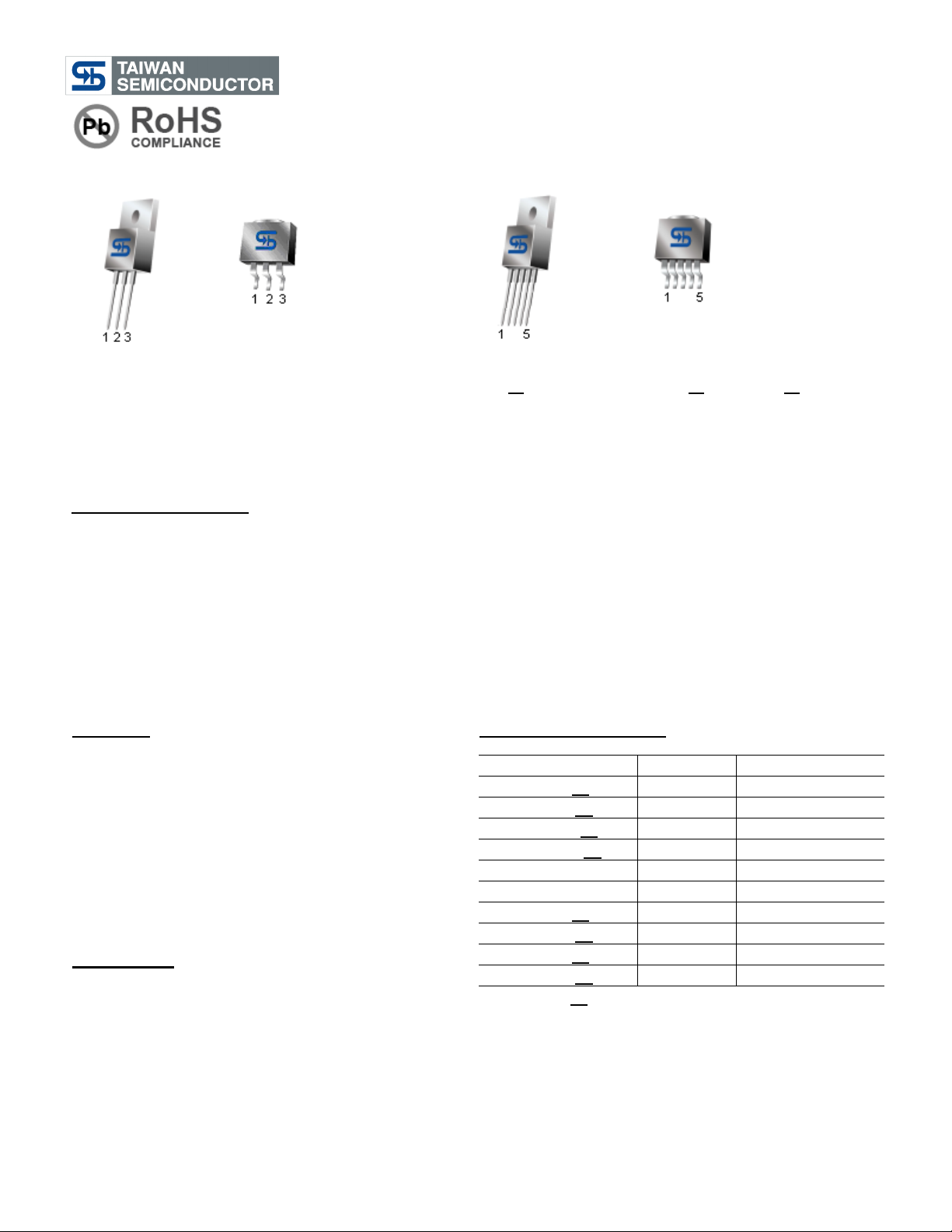
TO-220
TO-263
(D2PAK)
TO-220-5L
TO-263-5L
(D2PAK)
General Description
TS39300/1/2/3/4 are 3A ultra low dropout linear voltage regulators that provide low voltage, high current output with a
minimum of external components. The TS3930x series offers extremely low dropout (typically 400mV at 3A) and low
quiescent current (typically 36mA at 3A).
TS39300/1/2/3/4 is ideal for PC add-in cards that need to convert from standard 3.3V to 2.5V or 2.5V to 1.8V. A
guaranteed maximum dropout voltage of 500mV over all operating conditions allows the TS39300/1/2/3/4 to provide
2.5V from a supply as low as 3V, and 1.8V from a supply as low as 2.5V. The TS39300/1/2/3/4 also has fast transient
response for heavy switching applications. The device requires only 47uF of output capacitor to maintain stability and
achieve fast transient response.
On the TS39300/1/2/3/4, the enable pin may be tied to input voltage if it is not required for enable control.
Features
● Dropout voltage typically 0.4V @Io=3A
● Output Current up to 3A
● Low Ground Current
● Extremely Fast Transient Response
● Current Limit & Thermal Shutdown
● Reversed Leakage & Reverse Battery Protection
● Error Flag Signals Output (TS39301 only)
● Adjustable Version (TS39302 only)
● Output Voltage Sense (TS39303/4 only)
Application
● PowerPCTM Power Supplies
● Battery Powered Equipment
● Consumer and Personal Electronics
● High Efficiency Linear Power Supplies
● SMPS Post Regulator and DC to DC Modules
● High-efficiency Post Regulator for Switching Supply
● Low Voltage Microcontrollers and Digital Logic
Ordering Information
Part No.
Package
Packing
TS39300CZxx C0
TO-220
50pcs / Tube
TS39300CMxx RN
TO-263
800pcs / 13” Reel
TS39301CZ5xx C0
TO-220-5L
50pcs / Tube
TS39301CM5xx RN
TO-263-5L
800pcs / 13” Reel
TS39302CZ5 C0
TO-220-5L
50pcs / Tube
TS39302CM5 RN
TO-263-5L
800pcs / 13” Reel
TS39303CZxx C0
TO-220-5L
50pcs / Tube
TS39303CMxx RN
TO-263-5L
800pcs / 13” Reel
TS39304CZxx C0
TO-220-5L
50pcs / Tube
TS39304CMxx RN
TO-263-5L
800pcs / 13” Reel
Note: Where xx denotes voltage option, available are
50=5V, 33=3.3V, 25=2.5V, 18=1.8V
Contact to factory for addition output voltage option.
Pin Definition:
TS39301xx
TS39302
TS39303xx
TS39304xx
1. Enable
1. Enable
1. Enable
1. Input
2. Input
2. Input
2. Input
2. Enable
3. Ground
3. Ground
3. Ground
3. Ground
4. Output
4. Output
4. Output
4. N/C
5. Flag
5. Adjust
5. Sense
5. Output
Pin Definition:
TS39300
1. Input
2. Ground (tab)
3. Output
TS39300/1/2/3/4
3A Ultra Low Dropout Voltage Regulator
with Multi-Function
2/12 Version: A07
Absolute Maximum Rating (Note 1)
Supply Voltage
VIN
-20V ~ +20
V
Enable Voltage
VEN
+20
V
Storage Temperature Range
T
STG
-65 ~ +150
o
C
Lead Soldering Temperature (260oC)
5
S
ESD (Note 3)
Operating Rating (Note 2)
Operation Input Voltage
VIN (operate)
+2.25 ~ +16
V
Operation Enable Voltage
VEN (operate)
+2.25 ~ +16
V
Power Dissipation (Note 4)
PD
Internally Limited
W
Operating Junction Temperature Range
TJ
-40 ~ +125
o
C
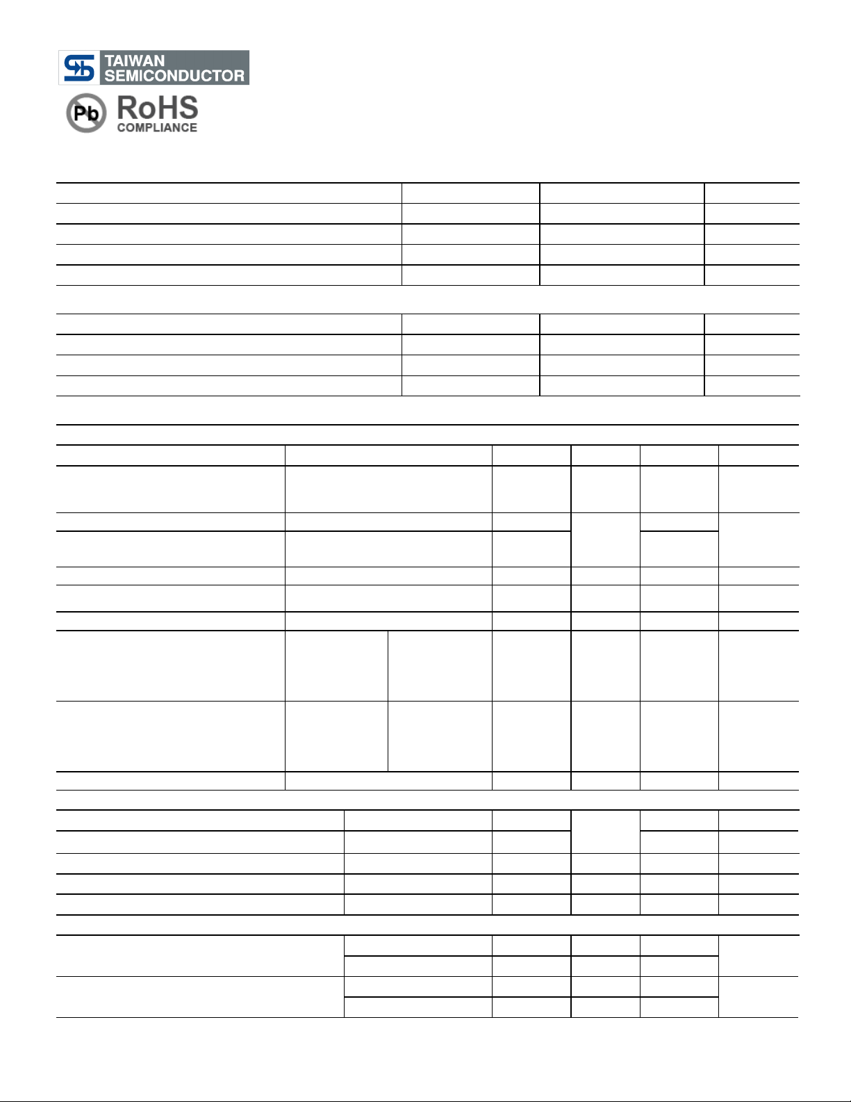
Electrical Characteristics
VIN = V
OUT
+ 1V, VIN =2.5V for fixed reference output voltage, Venable= 2.25V, Ta = 25oC, unless otherwise specified.
Parameter
Conditions
Min
Typ
Max
Unit
Fixed Output Voltage
10mA ≤ IL ≤ 3A,
Vo+1V ≤ VIN ≤ 8V
0.980|Vo|
V
OUT
1.020|Vo|
V
Fixed Reference Output Voltage
IL=10mA
0.980|Vo|
1.020|Vo|
Fixed Reference Output Voltage
10mA ≤ IL ≤ 3A,
2.5V ≤ VIN ≤ 8V
0.970|Vo|
1.24
(V
REF
)
1.030|Vo|
V
Line Regulation
IL=10mA, Vo+1V ≤ VIN ≤ 8V
--
0.05
0.5
%
Load Regulation
VIN =Vout+1V, 10mA≤IL≤3A
--
0.2
1.0
%
Output Voltage Temp. Coefficient
--
40
100
ppm/ oC
Dropout Voltage (Note 5)
Δ V
OUT
= -1%
IL=100mA
IL=750mA
IL=1.5A
IL=3A
--
--
--
--
65
185
250
400
200
--
--
550
mV
Quiescent Current (Note 6)
VIN=V
OUT
+1V
IL=100mA
IL=750mA
IL=1.5A
IL=3A
--
--
--
6
10
17
45
10
20
--
--
mA
Current Limited
V
OUT
=0, VIN =V
OUT
+1V
--
4.5
--
A
Reference (TS39302)
Reference Voltage
0.980|Vo|
1.020|Vo|
Reference Voltage
(Note 7)
0.970|Vo|
1.24
1.030|Vo|
V
Adjust Pin Bias Current
--
40
120
nA
Reference Voltage Temp. Coefficient
(Note 8)
--
20
--
ppm/ oC
Adjust Pin Bias Current Temp. Coefficient
--
0.1
--
nA/ oC
Enable Input (TS39301/2/3/4)
Low (OFF)
--
--
0.8
Input Logic Voltage
High (ON)
2.25
--
--
V
VEN =2.25V
--
--
75
Enable Pin Input Current
VEN =0.8V
--
--
4
uA
TS39300/1/2/3/4
3A Ultra Low Dropout Voltage Regulator
with Multi-Function
3/12 Version: A07
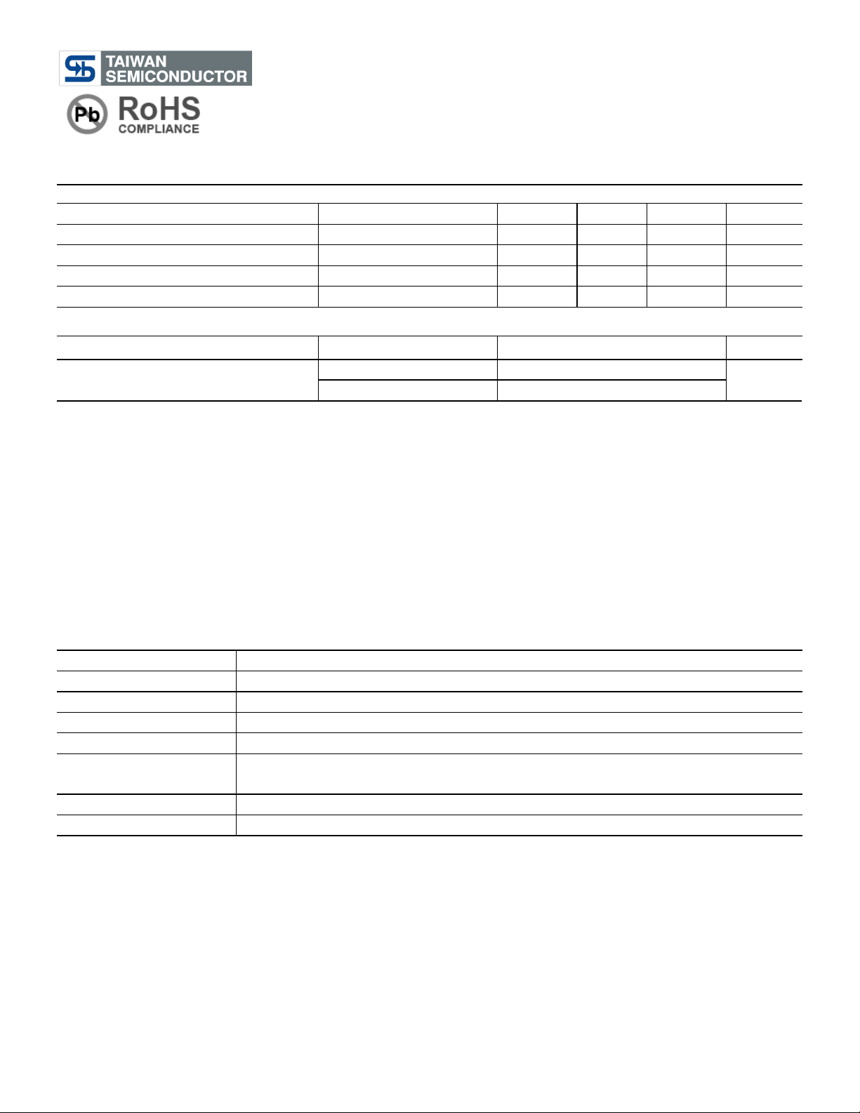
Electrical Characteristics (Continue)
Flag Output (TS39301)
Output Leakage Current
VOH=16V
--
-- 2 uA
Output Low Voltage (Note 9)
VIN=0.9 * V
OUT
, IOL=250uA
--
--
400
mV
Upper Threshold Voltage
% of V
OUT
--
--
99
%
Lower Threshold Voltage
% of V
OUT
93
--
--
%
Hysteresis
-- 1 --
%
Thermal Performance
Condition
Package type
Typ
Unit
TO-220 / TO-220-5L
80
Thermal Resistance
Junction to Case
TO-263 / TO-263-5L
80
o
C/W
Note 1. Exceeding the absolute maximum ratings may be damaged the device.
Note 2. The device is not guaranteed to function outside its operating rating.
Note 3. Devices are ESD sensitive. Handling precautions recommended.
Note 4. P
D(max)
= (T
J(max)
- Ta) + ӨJA, where ӨJA depends upon the printed circuit layout. See ”Applications Information”.
Note 5. Output voltage temperature coefficient is ΔV
OUT (worst case)
+(T
J(max)
– T
J(MIN)
) where T
J(max)
is +125oC and T
JMIN)
is
-40oC.
Note 6. V
DROP
= VIN - V
OUT
when V
OUT
decreases to 99% of its nominal output voltage with VIN = V
OUT
+ 1. For output
voltages below 2.5V, dropout voltage is the input-to-output voltage differential with the minimum input voltage
being 2.5V. Minimum input operating voltage is 2.5V
Note 7. I
GND
is the quiescent current. IIN = I
GND
+ I
OUT
Note 8. VEN <0.8V, VIN <8V and V
OUT
=0
Note 9. For 1.8V device, VIN = 2.25V (device is in dropout)
Pin Description
Pin Configuration
Pin Description
Enable
TTL/COMS compatible input. Logic high is enable; logic low or open is shutdown
Input
Unregulated input: +16V maximum supply
Ground
Ground: Ground pin and TAB / heat sink are internally connected.
Output
Regulator output
Flag (fixed voltage)
Error Flag (output): Open-collector output. Active low indicates an output fault condition,
if no used, leave open.
Feed Back (adjustable)
Adjustment input: Feedback input. Connect to resistive voltage-divider network.
Sense
Sense pin is the input to the error amplifier
TS39300/1/2/3/4
3A Ultra Low Dropout Voltage Regulator
with Multi-Function
4/12 Version: A07
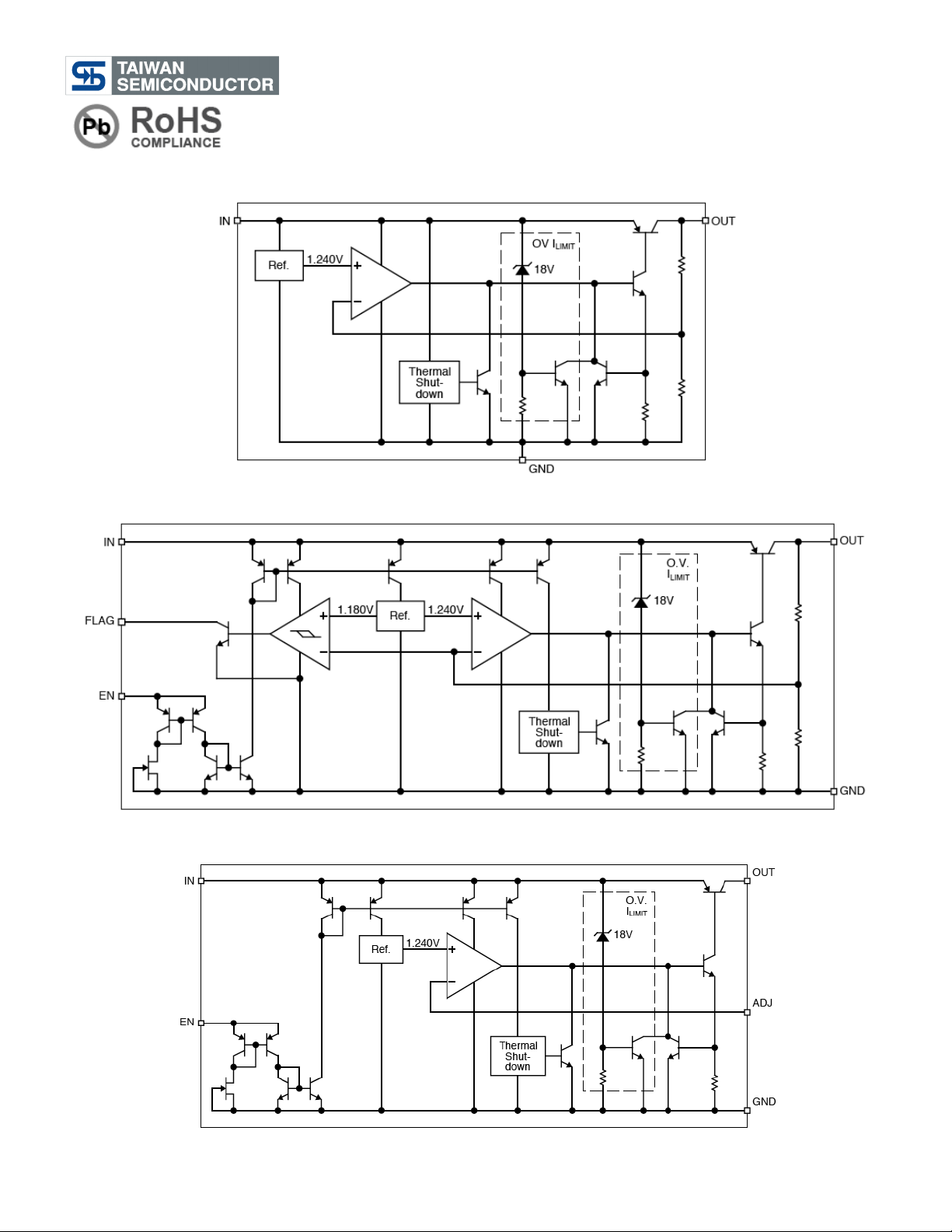
Functional Diagram
TS39300 Fixed Regulator Block Diagram
TS39301/3/4 Fixed Regulator with Flag, Sense and Enable Block Diagram
TS39302 Adjustable Regulator Block Diagram

TS39300/1/2/3/4
3A Ultra Low Dropout Voltage Regulator
with Multi-Function
5/12 Version: A07
Application Information
The TS39300/1/2/3/4 are high performance with low dropout voltage regulator suitable for moderate to high current
and voltage regulator application. Its 630mV dropout voltage at full load and over temperature makes it especially
valuable in battery power systems and as high efficiency noise filters in post regulator applications. Unlike normal NPN
transistor design, where the base to emitter voltage drop and collector to emitter saturation voltage limit the minimum
dropout voltage, dropout performance of the PNP output of these devices is limited only by low VCE saturation voltage.
The TS39300/1/2/3/4 is fully protected from damage due to fault conditions. Linear current limiting is provided. Output
current during overload conditions is constant. Thermal shutdown the device when the die temperature exceeds the
maximum safe operating temperature. Transient protection allows device survival even when the input voltage spikes
above and below nominal. The output structure of these regulators allows voltages in excess of the desired output
voltage to be applied without reverse current flow.
Output Capacitor Requirement
The TS39300/1/2/3/4 requires an output capacitor to maintain stability and improve transient response is necessary.
The value of this capacitor is dependent upon the output current, lower currents allow smaller capacitors.
TS39300/1/2/3/4 output capacitor selection is dependent upon the ESR of the output capacitor to maintain stability.
When the output capacitor is 10uF or greater, the output capacitor should have an ESR less than 2Ω. This will improve
transient response as well as promote stability. Ultra low ESR capacitors (<100mΩ), such as ceramic chip capacitors,
may promote instability. These very low ESR levels may cause an oscillation and/or under damped transient response.
A low ESR solid tantalum capacitor works extremely well and provides good transient response and stability over
temperature aluminum electrolytes can also be used, as long as the ESR of the capacitor is <2Ω. The value of the
output capacitor can be increased without limit. Higher capacitance values help to improve transient response and
ripple rejection and reduce output noise.
Input Capacitor Requirement
An input capacitor of 1uF or greater is recommended when the device is more than 4” away from the bulk AC supply
capacitance or when the supply is a battery. Small, surface mount, ceramic chip capacitors can be used for bypassing.
Larger values will help to improve ripple rejection by bypassing the input to the regulator, further improving the integrity
of the output voltage.
Minimum Load Current
The TS39300/1/2/3/4 is specified between finite loads. If the output current is too small leakage currents dominate and
the output voltage rises. A 10mA minimum load current is necessary for proper regulation.
Adjustable Regulator Design
The adjustable regulator versions (TS39302) is allow to programming the output voltage anywhere between 1.25 and
the 16V maximum operating rating of the family.
Two resistors are used. Resistors can be quite large up to 1MΩ, because of the very high input impedance and low
bias current of the sense comparator, the resistor values are calculated by:
Where V
OUT
is the desired output voltage. Above application circuit shows component definition. Applications with
widely varying load currents may scale the resistors to draw the minimum load current required for proper operation.
TS39300/1/2/3/4
3A Ultra Low Dropout Voltage Regulator
with Multi-Function
6/12 Version: A07
Application Information (Continue)
Enable Input
TS39301/2/3/4 versions feature an active-high enable (EN) input that allows ON/OFF control of the regulator. Current
drain reduces to “zero” when the device is shutdown, with only micro-amperes of leakage current. The EN input has
TTL/CMOS compatible thresholds for simple interfacing with logic interfacing. EN may be directly tied to VIN and pulled
up to the maximum supply voltage.
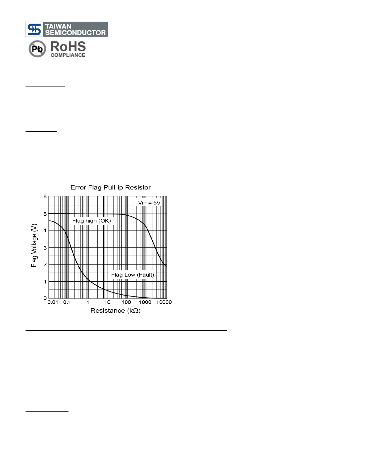
Error Flag
TS39301 versions feature an Error Flag, which looks at the output voltage and signals an error condition when this
voltage drops 5% below its expected value. The error flag is an open-collector output that pulls low under fault
conditions. It may sink 10mA. Low output voltage signifies a number of possible problems, including an over-current
fault (the device is in current limit) or low input voltage. The flag output is inoperative during over temperature
shutdown conditions. A pull-up resistor from error flag to either VIN or V
OUT
is required for proper operation. For
information regarding the minimum and maximum values of pull-up resistance, refer the graph as follow:
Transient Response and 3.3V to 2.5V or 2.5V to 1.8V Conversion
TS39300/1/2/3/4 has excellent transient response to variations in input voltage and load current. The device have
been designed to respond quickly to load current variations and input voltage variations. Large output capacitors are
not required to obtain this performance. A standard 10uF output capacitor, preferably tantalum, is all that is required.
Larger values help to improve performance even further. By virtue of its low dropout voltage, this device does not
saturate into dropout as readily as similar NPN base designs. When converting from 3.3V to 2.5V or 2.5V to 1.8V, the
NPN based regulators are already operating in dropout, with typical dropout requirements of 1.2V or greater,. To
convert down to 2.5V or 1.8V without operating in dropout, NPN based regulators require an input voltage of 3.7V at
the very least. The TS39300/1/2/3/4 regulator will provide excellent performance with an input as low as 3.0V or 2.5V
respectively. This gives the PNP based regulators a distinct advantage over older, NPN based linear regulators.
Output Sense
Sense pin can be connected to the load and traces the load voltage, TS39303/4 will adjust the output voltage to
maintain the load at expected voltage.

TS39300/1/2/3/4
3A Ultra Low Dropout Voltage Regulator
with Multi-Function
7/12 Version: A07
Application Information (Continue)
Thermal Characteristics
TS39300/1/2/3/4 linear regulators are simple to use, the most complicated design parameters to consider are
thermal characteristics, thermal design requires the following application specification parameters:
Maximum ambient temperature, T
A
Output current, I
OUT
Output voltage, V
OUT
Input voltage, V
IN
Calculate the power dissipation of the regulator from these numbers and the device parameters from this datasheet,
where the ground current is taken from data sheet.
PD = (VIN – V
OUT
) x I
OUT
+ VIN x I
GND
The heat sink thermal resistance is determined by:
ӨSA = (T
J(MAX)
– TA) / PD – (ӨJC + ӨCS)
Where T
J(MAX)
≤ 125
o
C and Ө
CS
is between 0
o
C and 2oC/W. The heat sink may by significantly reduced in
applications where the minimum input voltage is know and is large compared with the dropout voltage and distribute
the heat between this resistor and the regulator. The low dropout properties of vertical PNP regulators allow
significant reductions in regulator power dissipation and the associated heat sink without compromising performance.
When this technique is employed, a capacitor of at least 1uF is needed directly between the input and regulator
ground.
Typical Application Circuit
2.5V/3A Regulator
2.5V/3A Regulator with Error Flag

TS39300/1/2/3/4
3A Ultra Low Dropout Voltage Regulator
with Multi-Function
8/12 Version: A07
TO-220 Mechanical Drawing
TO-220 DIMENSION
MILLIMETERS
INCHES
DIM
MIN
MAX
MIN
MAX
A
10.000
10.500
0.394
0.413
B
3.740
3.910
0.147
0.154
C
2.440
2.940
0.096
0.116
D - 6.350
-
0.250
E
0.381
1.106
0.015
0.040
F
2.345
2.715
0.092
0.058
G
4.690
5.430
0.092
0.107
H
12.700
14.732
0.500
0.581
I
8.382
9.017
0.330
0.355
J
14.224
16.510
0.560
0.650
K
3.556
4.826
0.140
0.190
L
0.508
1.397
0.020
0.055
M
27.700
29.620
1.060
1.230
N
2.032
2.921
0.080
0.115
O
0.255
0.610
0.010
0.024
P
5.842
6.858
0.230
0.270
TS39300/1/2/3/4
3A Ultra Low Dropout Voltage Regulator
with Multi-Function
9/12 Version: A07
TO-263 Mechanical Drawing
TO-263 DIMENSION
MILLIMETERS
INCHES
DIM
MIN
MAX
MIN
MAX
A
10.000
10.500
0.394
0.413
B
14.605
15.875
0.575
0.625
C
0.508
0.991
0.020
0.039
D
2.420
2.660
0.095
0.105
E
4.064
4.830
0.160
0.190
F
1.118
1.400
0.045
0.055
G
0.450
0.730
0.018
0.029
H
8.280
8.800
0.325
0.346
I
1.140
1.400
0.044
0.055
J
1.480
1.520
0.058
0.060

TS39300/1/2/3/4
3A Ultra Low Dropout Voltage Regulator
with Multi-Function
10/12 Version: A07
TO-220-5L Mechanical Drawing
TO-220-5L DIMENSION
MILLIMETERS
INCHES
DIM
MIN
MAX
MIN
MAX
A
10.00
10.50
0.394
0.413
B
3.240
4.440
0.128
0.175
C
2.440
2.940
0.096
0.116
D
0.260
1.020
0.010
0.040
E
1.570
1.830
0.062
0.072
F
13.31
14.13
0.524
0.556
G
4.475
5.225
0.176
0.206
H
1.170
1.370
0.046
0.054
I
27.60
29.44
1.087
1.159
J
2.175
2.925
0.086
0.115
K
0.297
0.477
0.012
0.019
L
8.280
8.800
0.326
0.346
M
6.010
6.510
0.237
0.256
N
14.29
15.31
0.563
0.603

TS39300/1/2/3/4
3A Ultra Low Dropout Voltage Regulator
with Multi-Function
11/12 Version: A07
TO-263-5L Mechanical Drawing
TO-263-5L DIMENSION
MILLIMETERS
INCHES
DIM
MIN
MAX
MIN
MAX
A
9.70
10.54
0.382
0.415
B
14.60
15.87
0.575
0.625
C
0.69
0.94
0.027
0.037
D
1.524
2.032
0.060
0.080
E
4.30
4.70
0.169
0.185
F
1.22
1.40
0.048
0.055
G
2.24
2.82
0.088
0.111
H
0.36
0.56
0.014
0.022
I
8.50
9.20
0.330
0.362
J
1.40 MAX
0.055 MAX

TS39300/1/2/3/4
3A Ultra Low Dropout Voltage Regulator
with Multi-Function
12/12 Version: A07
Notice
Specifications of the products displayed herein are subject to change without notice. TSC or anyone on its behalf,
assumes no responsibility or liability for any errors or inaccuracies.
Information contained herein is intended to provide a product description only. No license, express or implied, to any
intellectual property rights is granted by this document. Except as provided in TSC’s terms and conditions of sale for
such products, TSC assumes no liability whatsoever, and disclaims any express or implied warranty, relating to sale
and/or use of TSC products including liability or warranties relating to fitness for a particular purpose, merchantability,
or infringement of any patent, copyright, or other intellectual property right.
The products shown herein are not designed for use in medical, life-saving, or life-sustaining applications. Customers
using or selling these products for use in such applications do so at their own risk and agree to fully indemnify TSC for
any damages resulting from such improper use or sale.
 Loading...