


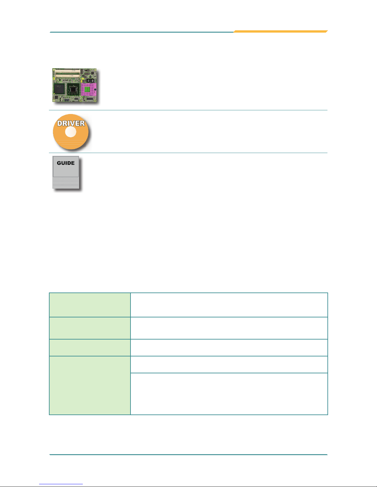
EmETXe-i9652
COM Express CPU Module
User’s Manual
Version 1.2
2011.06

This page is intentionally left blank.

Index
- i -
Table of Contents
Chapter 1 - Introduction ............................................ 1
1.1 Copyright Notice .......................................................2
1.2 Declaration of Conformity ........................................2
1.3 About This User’s Manual ........................................3
1.4 Warning ......................................................................3
1.5 Replacing the Lithium Battery .................................3
1.6 Technical Support .....................................................4
1.7 Warranty .....................................................................4
1.8 Packing List ...............................................................5
1.9 Ordering Information ................................................5
1.10 Specifications ..........................................................6
1.11 Board Dimensions...................................................7
Chapter 2 - Installation ..............................................9
2.1 What is “ COM Express ”? .....................................10
2.2 Block Diagram ........................................................11
2.3 Jumpers and Connectors .......................................12
2.4 COM Express AB Connector ..................................13
2.5 COM Express CD Connector..................................15
2.6 The Installation Paths of CD Driver .......................17
Chapter 3 - BIOS ......................................................19
3.1 BIOS Main Setup .....................................................20
3.2 Advanced Settings ..................................................21
3.2.1 CPU Configuration ............................................22
3.2.2 IDE Configuration .............................................24
3.2.3 Floppy Configuration ........................................25
3.2.4 Super IO Configuration ....................................26
3.2.5 Hardware Health Configuration .......................28
3.2.6 ACPI Configuration ...........................................29
3.2.7 AHCI Configuration ...........................................30
3.2.8 APM Configuration ............................................31
3.2.9 MPS Configuration ............................................33
3.2.10 USB Configuration ..........................................34

Index
3.2.11 Remote Access Configuration .......................36
3.3 Advanced PCI/PnP Settings ..................................37
3.4 Boot Settings ...........................................................39
3.4.1 Boot Settings Configuration ............................40
3.5 Security ....................................................................41
3.6 Advanced Chipset Settings ....................................43
3.6.1 North Bridge Chipset Configuration ...............43
3.6.2 South Bridge Chipset Configuration ...............46
3.7 Exit Options .............................................................48
3.8 Beep Sound codes list............................................53
3.8.1 Boot Block Beep Codes ...................................53
3.8.2 POST BIOS Beep Codes ...................................53
3.8.3 Troubleshooting POST BIOS Beep Codes .....54
Appendix .................................................................. 67
Appendix A: I/O Port Address Map ..............................68
Appendix B: BIOS Memory Map ..................................69
Appendix C: Interrupt Request Lines (IRQ) ................70
Appendix D: Digital I/O Setting ....................................71
- ii -

Introduction
- 1 -
1Chapter 1
Introduction
Chapter 1 - Introduction

Introduction
- 2 -
1.1 Copyright Notice
All Rights Reserved.
The information in this document is subject to change without prior notice in
order to improve the reliability, design and function. It does not represent a
commitment on the part of the manufacturer.
Under no circumstances will the manufacturer be liable for any direct, indirect,
special, incidental, or consequential damages arising from the use or inability
to use the product or documentation, even if advised of the possibility of such
damages.
This document contains proprietary information protected by copyright.
All rights are reserved. No part of this manual may be reproduced by any
mechanical, electronic, or other means in any form without prior written
permission of the manufacturer.
1.2 Declaration of Conformity
CE
This product has passed the CE test for environmental specications when
shielded cables are used for external wiring. This kind of cable is available
from ARBOR. Please contact your local supplier for ordering information.
Test conditions for passing included the equipment being operated within an
industrial enclosure. In order to protect the product from being damaged by
ESD (Electrostatic Discharge) and EMI leakage, we strongly recommend the
use of CE-compliant industrial enclosure products.
FCC Class A
This device complies with Part 15 of the FCC Rules. Operation is subject
to the following two conditions : (1) this device may not cause harmful
interference, and (2) this device must accept any interference received,
including interference that may cause undesired operation.
RoHS
ARBOR Technology Corp. certies that all components in its products are in
compliance and conform to the European Union’s Restriction of Use of Hazardous Substances in Electrical and Electronic Equipment (RoHS) Directive
2002/95/EC.
The above mentioned directive was published on 2/13/2003. The main purpose of the directive is to prohibit the use of lead, mercury, cadmium, hexavalent chromium, polybrominated biphenyls (PBB), and polybrominated diphenyl
ethers (PBDE) in electrical and electronic products. Member states of the EU

Introduction
- 3 -
are to enforce by 7/1/2006.
ARBOR Technology Corp. hereby states that the listed products do not contain unintentional additions of lead, mercury, hex chrome, PBB or PBDB that
exceed a maximum concentration value of 0.1% by weight or for cadmium
exceed 0.01% by weight, per homogenous material. Homogenous material
is dened as a substance or mixture of substances with uniform composition
(such as solders, resins, plating, etc.). Lead-free solder is used for all terminations (Sn(96-96.5%), Ag(3.0-3.5%) and Cu(0.5%)).
1.3 About This User’s Manual
This user’s manual provides general information and installation instructions
about the product. This User’s Manual is intended for experienced users and
integrators with hardware knowledge of personal computers. If you are not
sure about any description in this booklet. please consult your vendor before
further handling.
1.4 Warning
Single Board Computers and their components contain very delicate
Integrated Circuits (IC). To protect the Single Board Computer and its
components against damage from static electricity, you should always follow
the following precautions when handling it :
1. Disconnect your Single Board Computer from the power source when you
want to work on the inside.
2. Hold the board by the edges and try not to touch the IC chips, leads or circuitry.
3. Use a grounded wrist strap when handling computer components.
4. Place components on a grounded antistatic pad or on the bag that comes
with the Single Board Computer, whenever components are separated from
the system.
1.5 Replacing the Lithium Battery
Incorrect replacement of the lithium battery may lead to a risk of explosion.
The lithium battery must be replaced with an identical battery or a battery type
recommended by the manufacturer.
Do not throw lithium batteries into the trash-can. It must be disposed of in
accordance with local regulations concerning special waste.

Introduction
- 4 -
1.6 Technical Support
If you have any technical difculties, please do not hesitate to call or e-mail our
customer service.
http://www.arbor.com.tw
E-mail:info@arbor.com.tw
1.7 Warranty
This product is warranted to be in good working order for a period of two years
from the date of purchase. Should this product fail to be in good working order
at any time during this period, we will, at our option, replace or repair it at no
additional charge except as set forth in the following terms. This warranty does
not apply to products damaged by misuse, modications, accident or disaster.
Vendor assumes no liability for any damages, lost prots, lost savings or any
other incidental or consequential damage resulting from the use, misuse of,
or inability to use this product. Vendor will not be liable for any claim made by
any other related party.
Vendors disclaim all other warranties, either expressed or implied, including
but not limited to implied warranties of merchantability and tness for a
particular purpose, with respect to the hardware, the accompanying product’s
manual(s) and
written materials, and any accompanying hardware. This limited
warranty gives you specic legal rights.
Return authorization must be obtained from the vendor before returned
merchandise will be accepted.
Authorization can be obtained by calling or
faxing
the vendor and
requesting a Return Merchandise Authorization (RMA)
number.
Returned
goods should always be accompanied by a clear problem
description.
Introduction
- 5 -
1.8 Packing List
1 x EmETXe-i9652 COM Express CPU Module
1 x Driver CD
1 x Quick Installation Guide
1.9 Ordering Information
EmETXe-i9652
Socket P Intel® Core™ 2 Duo/Celeron® M COM
Express CPU Module
HS-9455-C3
Heatsink w/ fan for socket type CPU module
(125 x 96 x 39 mm)
PBE-1700 COM Express evaluation board in ATX form factor
CBK-04-1700-00
Cable kit
1 x SATA cable
1 x COM cable
1 x FDD cable
1 x IDE cable
If any of the above items is damaged or missing, contact your vendor
immediately.

Introduction
- 6 -
1.10 Specifications
Form Factor COM Express Type 2 CPU Module
CPU
Intel® Core™ 2 Duo processor, up to 800MHz FSB
Intel® Celeron® M processor with 533/667MHz
FSB
Chipset Intel® GME965 + Intel® ICH8M
System Memory
2 x 200-pin DDR2 SO-DIMM sockets supporting
533/667MHz SDRAM up to 4GB
VGA/LCD Controller
Integrated Intel® Graphics Media Accelerator
X3100
Ethernet 1 x RTL8111 PCIe Gigabit Ethernet Controller
BIOS AMI PnP Flash BIOS
Serial ATA 3 x Serial ATA with 300MB/s HDD transfer rate
IDE Interface 1 x Ultra ATA, supports 2 IDE devices
Universal Serial Bus 8 x USB 2.0
Digital Input/Output 8-bit programmable Digital Input/Output
Expansion Interface
1 x PCI Express x16
5 x PCI Express x1
4 x PCI
Operation Temp. -20ºC ~ 70ºC (-4ºF ~ 158ºF)
Watchdog Timer 1 ~ 255 levels Reset
Dimension (L x W) 125 x 95 mm (4.9” x 3.7”)
Introduction
- 7 -
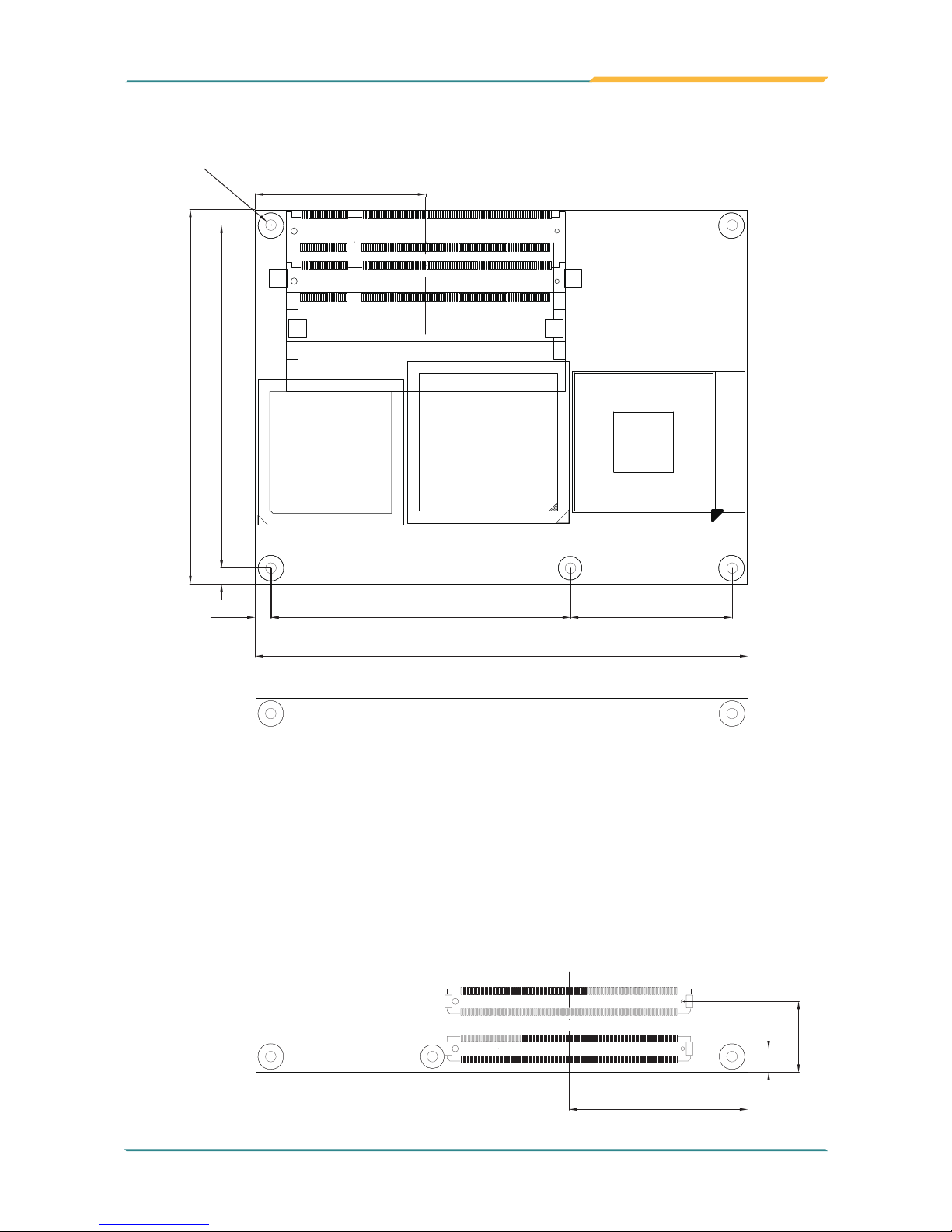
1.11 Board Dimensions
43.28
DIMM2
DIMM1
CPU Socket
87.00
4.00
95.00
Ø2.70
4.00
Unit: mm
76.00
125.00
41.00
45.35
18.00
6.00

Introduction
- 8 -
This page is intentionally left blank.

Installation
- 9 -
2Chapter 2
Installation
Chapter 2 - Installation

Installation
- 10 -
2.1 What is “ COM Express ”?
With more and more demands on small and embedded industrial boards, a
multi-functioned COM (Computer-on-Module) is the great one of the
solutions.
COM Express, board-to-board connectors consist of two rows of 220 pins
each.
Row AB, which is required, provides pins for PCI Express, SATA, LVDS, LCD
channel, LPC bus, system and power management, VGA, LAN, and power
and ground interfaces.
Row CD, which is optional, provides SDVO and legacy PCI and IDE signals
next to additional PCI Express, LAN and power and ground signals.
By the way, the target markets of COM will be focused on:
● Retail & Advertising
● Medical
● Test & Measurement
● Gaming & Entertainment
● Industrial & Automation
● Military & Government
● Security
Installation
- 11 -
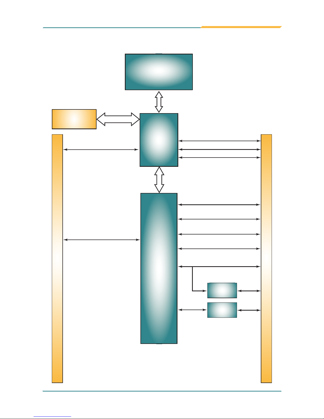
2.2 Block Diagram
PCI Bus
Connector CD
Mobile Intel®
GME965
Socket P Intel®
Celeron® M/Core™
2 Duo CPU
FSB
533/667/800MHz
2 x 200 pins DDRII
SO-DIMM socket
Intel®
ICH8-M
AC’97 Link
Dual Channel DDRII
Analog
R.G.B.
18-24-bit LVDS
TV-Out
LPC I/F
PCIe LAN
controller
Serial ATA I/F
IDE ATA I/F
USB I/F
DMI
I/F
Connector AB
PCIe*16
PCIe*1
Fintek
F75111R
DIO
Installation
- 12 -
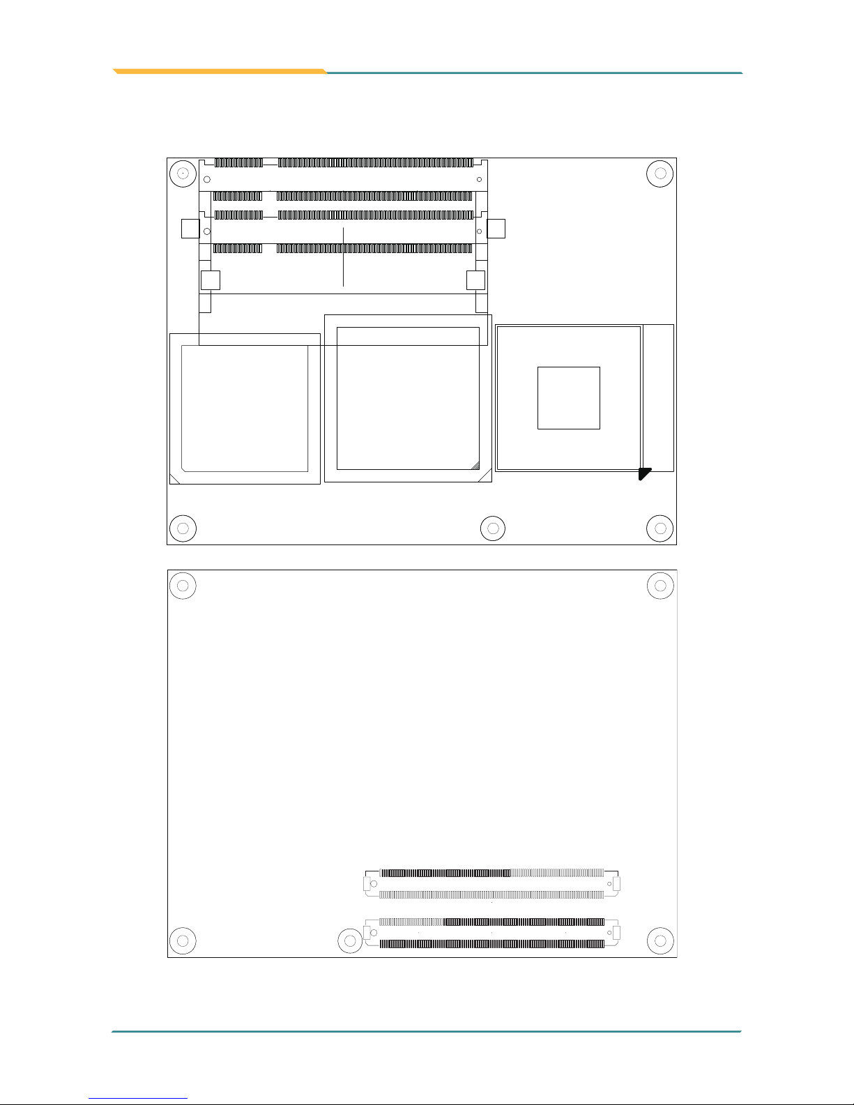
2.3 Jumpers and Connectors
DIMM2
DIMM1
CPU Socket
D1
C1
B1
A1
D110
C110
B110
A110

Installation
- 13 -
2.4 COM Express AB Connector
B1 GND GND A1
B2 GBE0_ACT# GBE0_MDI3- A2
B3 LPC_FRAME# GBE0_MDI3+ A3
B4 LPC_AD0 GBE0_LINK100# A4
B5 LPC_AD1 GBE0_LINK1000# A5
B6 LPC_AD2 GBE0_MDI2- A6
B7 LPC_AD3 GBE0_MDI2+ A7
B8 LPC_DRQ0# GBE0_LINK# A8
B9 LPC_DRQ1# GBE0_MDI1- A9
B10 LPC_CLK GBE0_MDI1+ A10
B11 GND GND A11
B12 PWRBTN# GBE0_MDI0- A12
B13 SMB_CK GBE0_MDI0+ A13
B14 SMB_DAT GBE0_CTREF A14
B15 SMB_ALERT# SUS_S3# A15
B16 N/C SATA0_TX+ A16
B17 N/C SATA0_TX- A17
B18 SUS_STAT# SUS_S4# A18
B19 N/C SATA0_RX+ A19
B20 N/C SATA0_RX- A20
B21 GND GND A21
B22 N/C SATA2_TX+ A22
B23 N/C SATA2_TX- A23
B24 PWR_OK SUS_S5# A24
B25 N/C SATA2_RX+ A25
B26 N/C SATA2_RX- A26
B27 WDT BATLOW# A27
B28 AC_SDIN2 ATA_ACT# A28
B29 AC_SDIN1 AC_SYNC A29
B30 AC_SDIN0 AC_RST# A30
B31 GND GND A31
B32 SPKR AC_BITCLK A32
B33 I2C_CK AC_SDOUT A33
B34 I2C_DAT BIOS_DISABLE# A34
B35 THRM# THRMTRIP# A35
B36 USB7- USB6- A36
B37 USB7+ USB6+ A37
B38 USB_4_5_OC# USB_6_7_OC# A38
B39 USB5- USB4- A39
B40 USB5+ USB4+ A40
B41 GND GND A41
B42 USB3- USB2- A42
B43 USB3+ USB2+ A43
B44 USB_0_1_OC# USB_2_3_OC# A44
B45 USB1- USB0- A45
B46 USB1+ USB0+ A46
B47 EXCD1_PERST# VCC_RTC A47
B48 EXCD1_CPPE# EXCD0_PERST# A48
B49 SYS_RESET# EXCD0_CPPE# A49
B50 CB_RESET# LPC_SERIRQ A50
B51 GND GND A51
B52 N/C N/C A52
B53 N/C N/C A53
B54 GPO1 GPI0 D54 A54
B55 N/C N/C A55

Installation
- 14 -
B56 N/C N/C A56
B57 GPO2 GND A57
B58 N/C N/C A58
B59 N/C N/C A59
B60 GND GND A60
B61 PCIE_RX2+ PCIE_TX2+ A61
B62 PCIE_RX2- PCIE_TX2- A62
B63 GPO3 GPI1 A63
B64 PCIE_RX1+ PCIE_TX1+ A64
B65 PCIE_RX1- PCIE_TX1- A65
B66 WAKE0# GND A66
B67 WAKE1# GPI2 A67
B68 PCIE_RX0+ PCIE_TX0+ A68
B69 PCIE_RX0- PCIE_TX0- A69
B70 GND GND A70
B71 LVDS_B0+ LVDS_A0+ A71
B72 LVDS_B0- LVDS_A0- A72
B73 LVDS_B1+ LVDS_A1+ A73
B74 LVDS_B1- LVDS_A1- A74
B75 LVDS_B2+ LVDS_A2+ A75
B76 LVDS_B2- LVDS_A2- A76
B77 N/C LVDS_VDD_EN A77
B78 N/C N/C A78
B79 LVDS_BKLT_EN N/C A79
B80 GND GND A80
B81 LVDS_B_CK+ LVDS_A_CK+ A81
B82 LVDS_B_CK- LVDS_A_CK- A82
B83
CKLVDS_BKLT_CTRL
LVDS_I2C_CK A83
B84 VCC_5V_SBY LVDS_I2C_DAT A84
B85 VCC_5V_SBY GPI3 A85
B86 VCC_5V_SBY KBD_RST# A86
B87 VCC_5V_SBY KBD_A20GATE A87
B88 RSVD PCIE0_CK_REF+ A88
B89 VGA_RED PCIE0_CK_REF- A89
B90 GND GND A90
B91 VGA_GRN RSVD B91 A91
B92 VGA_BLU RSVD A92
B93 VGA_HSYNC GPO0 A93
B94 VGA_VSYNC RSVD A94
B95 VGA_I2C_CK RSVD A95
B96 VGA_I2C_DAT GND A96
B97 TV_DAC_A VCC_12V A97
B98 TV_DAC_B VCC_12V A98
B99 TV_DAC_C VCC_12V A99
B100 GND GND A100
B101 VCC_12V VCC_12V A101
B102 VCC_12V VCC_12V A102
B103 VCC_12V VCC_12V A103
B104 VCC_12V VCC_12V A104
B105 VCC_12V VCC_12V A105
B106 VCC_12V VCC_12V A106
B107 VCC_12V VCC_12V A107
B108 VCC_12V VCC_12V A108
B109 VCC_12V VCC_12V A109
B110 GND GND A110
Installation
- 15 -
2.5 COM Express CD Connector
D1 GND GND C1
D2 IDE_D5 IDE_D7 C2
D3 IDE_D10 IDE_D6 C3
D4 IDE_D11 IDE_D3 C4
D5 IDE_D12 IDE_D15 C5
D6 IDE_D4 IDE_D8 C6
D7 IDE_D0 IDE_D9 C7
D8 IDE_REQ IDE_D2 C8
D9 IDE_IOW# IDE_D13 C9
D10 IDE_ACK# IDE_D1 C10
D11 GND GND C11
D12 IDE_IRQ IDE_D14 C12
D13 IDE_A0 IDE_IORDY C13
D14 IDE_A1 IDE_IOR# C14
D15 IDE_A2 PCI_PME# C15
D16 IDE_CS1# PCI_GNT2# C16
D17 IDE_CS3# PCI_REQ2# C17
D18 IDE_RESET# PCI_GNT1# C18
D19 PCI_GNT3# PCI_REQ1# C19
D20 PCI_REQ3# PCI_GNT0# C20
D21 GND GND C21
D22 PCI_AD1 PCI_REQ0# C22
D23 PCI_AD3 PCI_RESET# C23
D24 PCI_AD5 PCI_AD0 C24
D25 PCI_AD7 PCI_AD2 C25
D26 PCI_C/BE0# PCI_AD4 C26
D27 PCI_AD9 PCI_AD6 C27
D28 PCI_AD11 PCI_AD8 C28
D29 PCI_AD13 PCI_AD10 C29
D30 PCI_AD15 PCI_AD12 C30
D31 GND GND C31
D32 PCI_PAR PCI_AD14 C32
D33 PCI_SERR# PCI_C/BE1# C33
D34 PCI_STOP# PCI_PERR# C34
D35 PCI_TRDY# PCI_LOCK# C35
D36 PCI_FRAME# PCI_DEVSEL# C36
D37 PCI_AD16 PCI_IRDY# C37
D38 PCI_AD18 PCI_C/BE2# C38
D39 PCI_AD20 PCI_AD17 C39
D40 PCI_AD22 PCI_AD19 C40
D41 GND GND C41
D42 PCI_AD24 PCI_AD21 C42
D43 PCI_AD26 PCI_AD23 C43
D44 PCI_AD28 PCI_C/BE3# C44
D45 PCI_AD30 PCI_AD25 C45
D46 PCI_IRQC# PCI_AD27 C46
D47 PCI_IRQD# PCI_AD29 C47
D48 PCI_CLKRUN# PCI_AD31 C48
D49 PCI_M66EN PCI_IRQA# C49
D50 PCI_CLK PCI_IRQB# C50
D51 GND GND (FIXED) C51
D52 PEG_TX0+ PEG_RX0+ C52
D53 PEG_TX0- PEG_RX0- C53
D54 PEG_LANE_RV# TYPE0# C54
D55 PEG_TX1+ PEG_RX1+ C55
Installation
- 16 -
D56 PEG_TX1- PEG_RX1- C56
D57 TYPE2# TYPE1# C57
D58 PEG_TX2+ PEG_RX2+ C58
D59 PEG_TX2- PEG_RX2- C59
D60 GND GND C60
D61 PEG_TX3+ PEG_RX3+ C61
D62 PEG_TX3- PEG_RX3- C62
D63 RSVD RSVD C63
D64 RSVD RSVD C64
D65 PEG_TX4+ PEG_RX4+ C65
D66 PEG_TX4- PEG_RX4- C66
D67 GND RSVD C67
D68 PEG_TX5+ PEG_RX5+ C68
D69 PEG_TX5- PEG_RX5- C69
D70 GND GND C70
D71 PEG_TX6+ PEG_RX6+ C71
D72 PEG_TX6- PEG_RX6- C72
D73 SDVO_CLK SDVO_DATA C73
D74 PEG_TX7+ PEG_RX7+ C74
D75 PEG_TX7- PEG_RX7- C75
D76 GND GND C76
D77 IDE_CBLID# RSVD C77
D78 PEG_TX8+ PEG_RX8+ C78
D79 PEG_TX8- PEG_RX8- C79
D80 GND GND C80
D81 PEG_TX9+ PEG_RX9+ C81
D82 PEG_TX9- PEG_RX9- C82
D83 RSVD RSVD C83
D84 GND GND C84
D85 PEG_TX10+ PEG_RX10+ C85
D86 PEG_TX10- PEG_RX10- C86
D87 GND GND C87
D88 PEG_TX11+ PEG_RX11+ C88
D89 PEG_TX11- PEG_RX11- C89
D90 GND GND C90
D91 PEG_TX12+ PEG_RX12+ C91
D92 PEG_TX12- PEG_RX12- C92
D93 GND GND C93
D94 PEG_TX13+ PEG_RX13+ C94
D95 PEG_TX13- PEG_RX13- C95
D96 GND GND C96
D97 PEG_ENABLE# RSVD C97
D98 PEG_TX14+ PEG_RX14+ C98
D99 PEG_TX14- PEG_RX14- C99
D100 GND GND C100
D101 PEG_TX15+ PEG_RX15+ C101
D102 PEG_TX15- PEG_RX15- C102
D103 GND GND C103
D104 VCC_12V VCC_12V C104
D105 VCC_12V VCC_12V C105
D106 VCC_12V VCC_12V C106
D107 VCC_12V VCC_12V C107
D108 VCC_12V VCC_12V C108
D109 VCC_12V VCC_12V C109
D110 GND GND C110

Installation
- 17 -
2.6 The Installation Paths of CD Driver
Windows 2000 & XP
Driver Path
CHIPSET \CHIPSET\INF 9.11
LAN \ETHERNET\REALTEK\8111_WINXP_5764
VGA \GRAPHICS\INTEL_2K_XP_32\1432
Windows 7
Driver Path
CHIPSET \CHIPSET\INF 9.11
LAN Windows 7 built-in LAN driver
VGA \GRAPHICS\INTEL_WIN7_32\1930
\GRAPHICS\INTEL_WIN7_64\1930

Installation
- 18 -
This page is intentionally left blank.

BIOS
- 19 -
3Chapter 3
BIOS
Chapter 3 - BIOS
BIOS
- 20 -
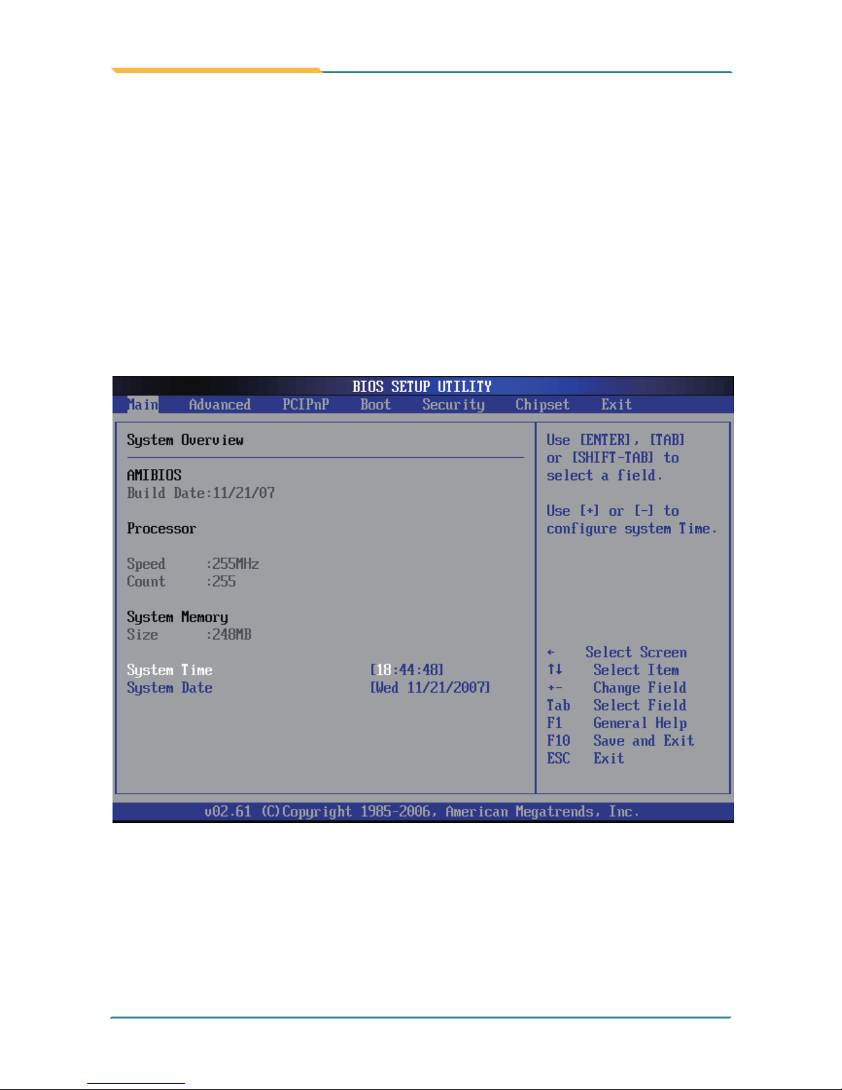
The AMI BIOS provides a setup utility program for specifying the system
congurations and settings. The BIOS ROM of the system stores the setup
utility.
When you turn on the computer, the AMI BIOS is immediately activated.
The Main displays system overview status. Use the left/right arrow keys to
highlight a particular conguration screen from the top menu bar or use the
down arrow key to access and congure the information below.
3.1 BIOS Main Setup
System Time
Set the system time.
The time format is: Hour : 00 to 23
Minute : 00 to 59
Second : 00 to 59
 Loading...