


EmCORE-i2702
3.5” Miniboard
User’s Manual
Version 1.0
2010.10

This page is intentionally left blank.

- i -
Index
Contents
Chapter 1 - Introduction ............................................ 1
1.1 Copyright Notice .........................................................2
1.2 About this User’s Manual ...........................................2
1.3 Warning .......................................................................2
1.4 Replacing the Lithium Battery ...................................3
1.5 Technical Support .......................................................3
1.6 Warranty ......................................................................4
1.7 Packing List.................................................................5
1.8 Ordering Information ..................................................5
1.9 Specications .............................................................6
1.10 Board Dimensions ....................................................7
1.11 Installing the Memory ...............................................8
Chapter 2 - Installation ..............................................9
2.1 Block Diagram...........................................................10
2.2 Jumpers and Connectors ........................................11
Jumpers ............................................................................12
CMOS Jumper Settings (JBAT1)...........................12
CF Card Select (J2) ................................................13
LCD Power (JVLCD1) .............................................14
COM2 RS-232/422/485 Slect (JRS2) .....................15
Connectors .......................................................................16
External SMB Connector (JSMB1) .......................16
FRONT PANEL (JFRT1) .........................................17
Serial ATA (SATA1/SATA2) .....................................18
RS-422/485 Serial Port (JCOM2) ...........................19
RS-232/422/485 Serial Port (COM2) ......................20
SATA Power Connector (J8) ..................................21
3DUDOOHO3RUWConnector (LPT).............................22
LED for Ethernet (CN2) ..........................................23
LAN Connector (LAN2) ..........................................24
Audio Connector (AUDIO1) ...................................25
USB Connector (USB2) .........................................26

- ii -
PWR-ATX Connector (PWR1/2) .............................27
ATX Feature Connector (PWR3) ...........................28
AT Power Switch (JPWR1) ....................................29
TV Connector (TV1) ...............................................30
INVERTOR Connector (INV1) ................................31
LVDS LCD Connector (LVDS1) ..............................32
Digital I/O (DIO1) ....................................................33
FAN Connector (SYSF1) ........................................34
2.3 The Installation Paths of CD Driver.........................35
Chapter 3 - BIOS ......................................................36
3.1 BIOS Introduction .....................................................37
3.2 BIOS Setup ................................................................38
3.3 Standard CMOS Features ........................................39
3.4 Advance BIOS Features ...........................................42
3.5 Advanced Chipset Features ....................................44
3.6 Integrated Peripherals ..............................................46
3.7 Power Management Setup .......................................50
3.8 PNP/PCI Congurations ...........................................52
3.9 PC Health Status .......................................................53
3.10 Load Optimized Defaults .......................................54
3.11 Set Password .........................................................55
3.12 Save & Exit Setup ...................................................56
3.13 Exit Without Saving ................................................57
3.14 Award BIOS POST Codes ......................................58
Chapter 4 - Appendix ......................................... 62
4.1 I/O Port Address Map ...............................................63
4.2 Interrupt Request Lines (IRQ) ..................................64
4.3 BIOS memory mapping ............................................65
4.4 Watchdog Timer (WDT) Setting ...............................65
4.5 Digital I/O Setting ......................................................66
Index

- 1 -
Introduction
1Chapter 1
Introduction

- 2 -
Introduction
All Rights Reserved.
The information in this document is subject to change without prior notice in
order to improve the reliability, design and function. It does not represent a
commitment on the part of the manufacturer.
Under no circumstances will the manufacturer be liable for any direct, indirect,
special, incidental, or consequential damages arising from the use or inability
to use the product or documentation, even if advised of the possibility of such
damages.
This document contains proprietary information protected by copyright.
All rights are reserved. No part of this manual may be reproduced by any
mechanical, electronic, or other means in any form without prior written
permission of the manufacturer.
1.2 About this User’s Manual
This User’s Manual is intended for experienced users and integrators with
hardware knowledge of personal computers. If you are not sure about any
description in this User’s Manual, please consult your vendor before further
handling.
1.3 Warning
Single Board Computers and their components contain very delicate
Integrated Circuits (IC). To protect the Single Board Computer and its
components against damage from static electricity, you should always follow
the following precautions when handling it :
Disconnect your Single Board Computer from the power source when you
want to work on the inside.
Hold the board by the edges and try not to touch the IC chips, leads or
circuitry.
Use a grounded wrist strap when handling computer components.
Place components on a grounded antistatic pad or on the bag that came
with the Single Board Computer, whenever components are separated
from the system.
1.
2.
3.
4.
1.1 Copyright Notice

- 3 -
Introduction
1.4 Replacing the Lithium Battery
Incorrect replacement of the lithium battery may lead to a risk of explosion.
The lithium battery must be replaced with an identical battery or a battery type
recommended by the manufacturer.
Do not throw lithium batteries into the trash-can. It must be disposed of in
accordance with local regulations concerning special waste.
1.5 Technical Support
If you have any technical difculties, please do not hesitate to call or e-mail
our customer service.
http://www.arbor.com.tw
E-mail:info@arbor.com.tw

- 4 -
Introduction
1.6 Warranty
This product is warranted to be in good working order for a period of two years
from the date of purchase. Should this product fail to be in good working order
at any time during this period, we will, at our option, replace or repair it at no
additional charge except as set forth in the following terms. This warranty
does not apply to products damaged by misuse, modications, accident or
disaster.
Vendor assumes no liability for any damages, lost prots, lost savings or any
other incidental or consequential damage resulting from the use, misuse of,
or inability to use this product. Vendor will not be liable for any claim made by
any other related party.
Vendors disclaim all other warranties, either expressed or implied, including
but not limited to implied warranties of merchantibility and tness for a
particular purpose, with respect to the hardware, the accompanying product’s
manual(s) and written materials, and any accompanying hardware. This
limited warranty gives you specic legal rights.
Return authorization must be obtained from the vendor before returned
merchandise will be accepted. Authorization can be obtained by calling or
faxing the vendor and requesting a Return Merchandise Authorization (RMA)
number. Returned goods should always be accompanied by a clear problem
description.
- 5 -
Introduction
1.7 Packing List
1.8 Ordering Information
Before you begin installing your single board, please make sure that the following
materials have been shipped:
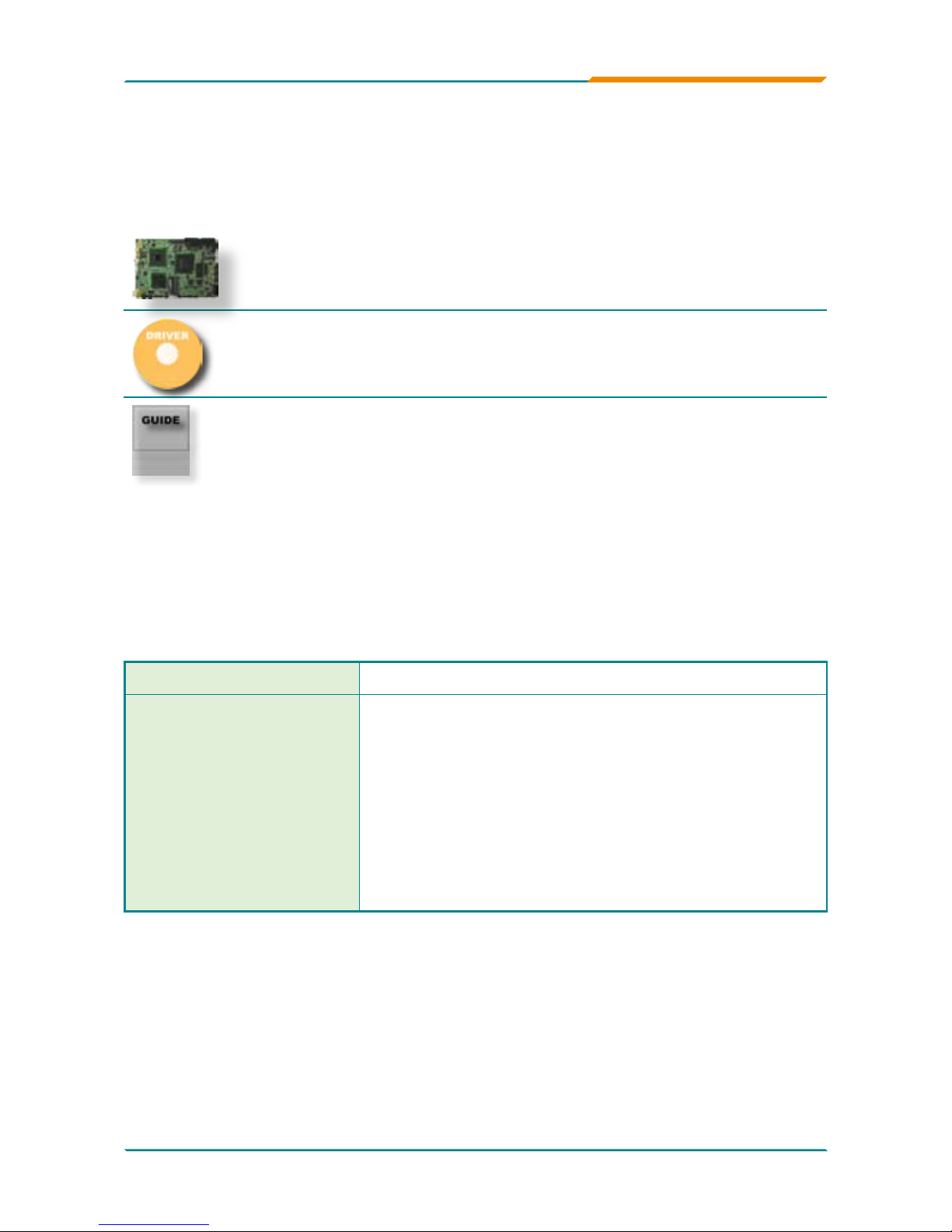
1 x EmCORE-i2702 3.5” Miniboard with heat sink
1 x Driver CD
1 x Quick Installation Guide
If any of the above items is damaged or missing, contact your vendor immediately.
EmCORE-i2702
Intel Atom™ N270 1.6GHz 3.5” Miniboard
CBK-8-3945-00
Cable Kit
1 x USB Cable
1 x KB & MS Cable
1 x Audio Cable
1 x SATA Cable
1 x COM Cable
1 x Print Cable
1 x LAN Cable
1 x IDE Cable

- 6 -
Introduction
1.9 Specications
Form Factor 3.5” Miniboard
CPU Intel®
Atom™ N270 CPU 1.6GHz with 533MHz FSB
Chipset Intel® 9
45GSE + Intel® ICH7M
System Memory 1 x 200-pin DDR2
533MHz SO-DIMM Socket Up to 1GB
VGA/ LCD
Controller
Integrated Intel Graphics Media
Accelerator 950, support
QXGA up to 2048 x 1546, LVDS support 18/36-bit, support
dual dispaly, TV-out
Ethernet 2 x Realtek 8111C PCIe Gigabit Ethernet controllers
I/O Chips ITE 8718F
BIOS
Phoenix-A
ward BIOS version 6.0PG, support 4MB SPI
Flash ROM
Audio
Realtek
ALC655 AC97 Audio CODEC, MIC-in/ Line-In/ Line-
Out
Serial Port
2 x COM ports
(COM1: RS-2
32, COM2: RS-232/422/485 selectable)
Digital I/O 4
-in / 4-out
Storage
2 x Serial
ATA 150MB/s HDD transfer rate
1 x ATA-66, support 2 ATAPI devices
1 x Floppy connector share with LPT port
Parallel Port 1 x LPT Port (SPP/EPP/ECP mode selectable)
KB/MS Support Standard PS/2 Keyboard and Mouse
Universal Serial Bus 4
x USB 2.0 ports
Expansion Interface Mini PCI
Watchdog Timer 1~2
55 levels (sec or min)
Hardware Monitor
Chip
Integrated in ITE8718F
RTC Support Real Time Clock
Power Connector DC +12V
Operation Temp. 0
o
C ~ 60oC
Dimension (L x W) 1
46 x 102 mm (5.7 ” x 4.0 ”)
- 7 -
Introduction
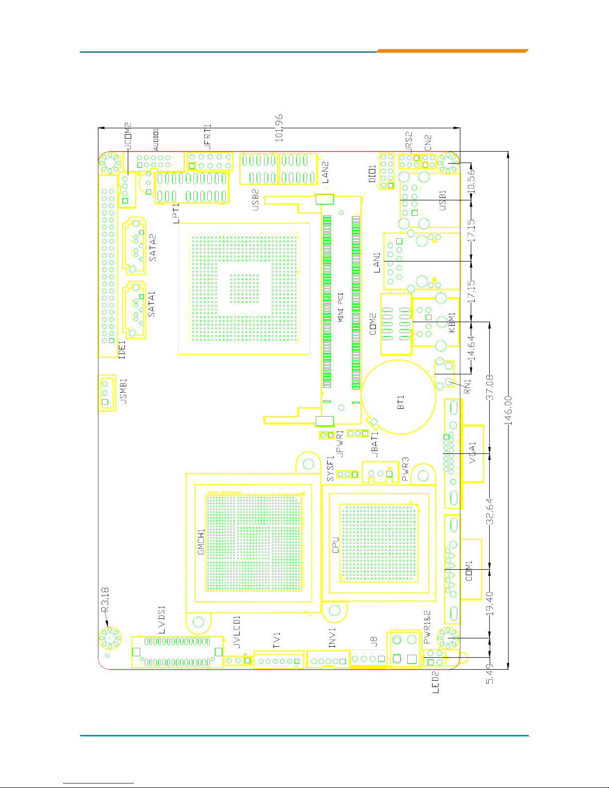
1.10 Board Dimensions
- 8 -
Introduction
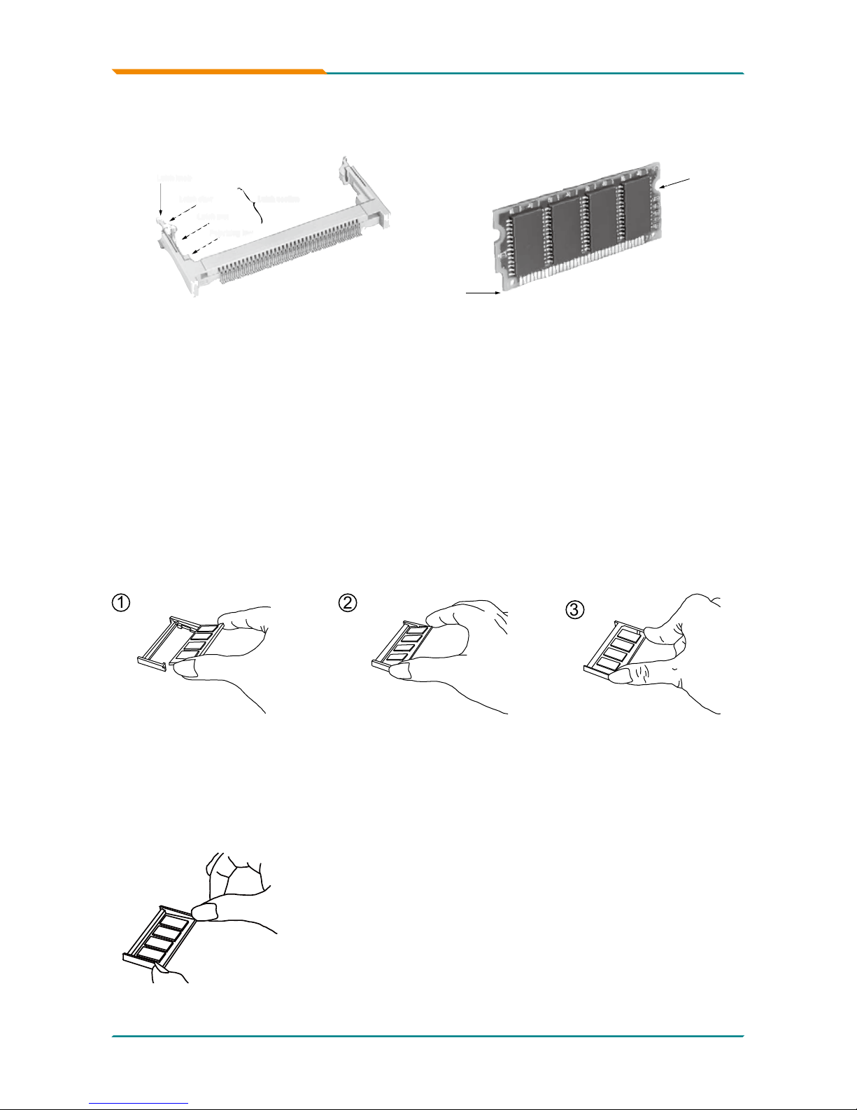
1.11 Installing the Memory
To install the Memory module, locate the Memory SO-DIMM slot on the board
and perform as below:
Adjust the socket polarizing key and the board key to the same direction.
Insert the board obliquely. Moreover, lay the board in parallel to the opening
at angle of 20
o
to 30o, and softly insert the board so as to hit the socket
bottom. Stopping insertion halfway will result in improper insertion.
Applying the board side notch in parallel to the socket bottom so that the
board position cannot be displaced, press the board side notch up, and x
it to the latch portion at both socket edges. Press the board side notch, and
release the notch with a snap “click” tone, if the printed board exceeds the
latch claw head.
1.
2.
3.
Side notch
Key
Latch knob
Latch claw
Latch section
Latch arm
Polarizing key
1
2
3
Procedures for board extraction
Apply the thumb nail to the latch knob at both socket edges. Forcibly widen
the latch knobs to right and left ways, and release the latch. Then draw the
board out along an angle where the board is raised.

- 9 -
Installation
2Chapter 2
Installation
Chapter 2 - Installation
- 10 -
Installation
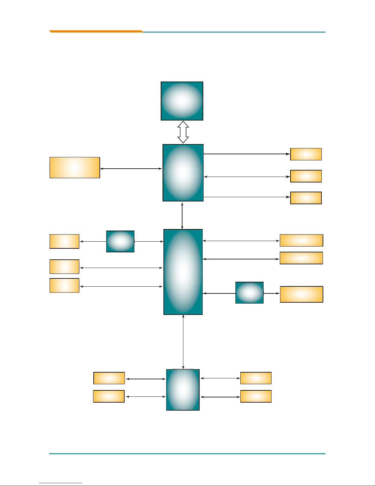
2.1 Block Diagram
TV-Out
Mobile
Intel®
945GSE
Intel®
Atom
N270
FSB
533MHz
400/533MHz
1 x 200-pin SO-DIMM
up to 1GB
Intel®
ICH7-M
AC Link
Single Channel DDR2
Analog
R.G.B.
Super IO
ITE 8718F
DMI
Serial ATA I/F
IDE ATA-66
2 x SATA
VGA
1 x IDE
PCIe*1 I/F
1 x Connector
1 x pin-header
COM ports
COM1,2
LPT1
LPT
KB/ MS
KB, MS
8-bit
Programmable
DIO
LPC
PCI Bus
Mini-PCI
Socket
AUDIO
2 x Realtek
8111C GbE
ALC655
AC97
CODEC
USB ports x 4
USB x 4
LVDS1
Dual-Channel 18/36-bit
- 11 -
Installation
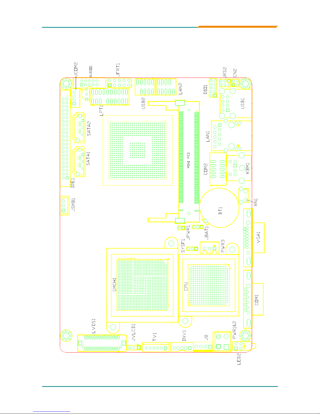
2.2 Jumpers and Connectors

- 12 -
Installation
Jumpers
CMOS Jumper Settings (JBAT1)
Type: onboard 3-pin 2.0mm header
Pin Mode
1-2 Keep CMOS
2-3 Clear CMOS
Default setting: Keep CMOS
INV1LED2
LVDS2
SYF1

- 13 -
Installation
CF Card Select (J2)
Type: onboard 2.0mm 3-pin headers.
Pin Mode
1 N/A
2-
3 ON Master
2-
3 OFF Slave

- 14 -
Installation
LCD Power (JVLCD1)
Type: onboard 3-pin 2.54mm header
Power
JVLCD1
5
V
1-2 ON
3
.3V
2-3 ON
Default setting: 3.3V

- 15 -
Installation
COM2 RS-232/422/485 Slect (JRS2)
Type: onboard 2.0mm 2x3-pin header
JRS2 Select 1-2 3-4 5-6
RS-232 ON OFF OFF
RS-422 OFF ON OFF
RS-
485 OFF OFF ON
Default setting: RS-232
LVDS2
JVLCD4
INV2
SATA2
Mini PCI
SYF1

- 16 -
Installation
External SMB Connector (JSMB1)
Type: onboard 2.0mm 3-pin header
Pin Description
1 SMB_DATA_MAIN
2 SMB_CLK_MAIN
3 ETX_SMI#
Connectors
JVLCD4
INV2

- 17 -
Installation
FRONT PANEL (JFRT1)
Type: 2.54mm 2x5-pin header
Pin Description Pin Description
1 RESET+ 2 RESET-
3 PLED+ 4 PLED-
5 HLED+ 6 HLED-
7 SPK+ 8 SPK-
9 PWRBTN+ 10 PWRBTN-
LVDS2
JVLCD4
INV2
SATA2

- 18 -
Installation
Serial ATA (SATA1/SATA2)
Type: Standard 7-pin SATA Connector
Pin Description
1 GND
2 TX+
3 TX-
4 GND
5 RX-
6 RX+
7 GND
LVDS2
JVLCD4
INV2

- 19 -
Installation
RS-422/485 Serial Port (JCOM2)
Type: onboard 2.0mm 1x4-pin header box
Pin
Description
1
RS
485RTX+
2
RS
485RTX-
3
RS
422RX+
4
RS
422RX-
JVLCD4
INV2

- 20 -
Installation
RS-232/422/485 Serial Port (COM2)
Type: onboard 2.0mm 10-pin wafer
Pin Description Pin Description
1 DCDB 2 RXB
3 TXB 4 DTRB
5 GND 6 DSRB
7 RTSB 8 CTSB
9 RIB
INV1LED2
LVDS2
JVLCD4
Mini PCI
SYF1

- 21 -
Installation
SATA Power Connector (J8)
Type: 1x4-pin SATA Power Connector
Pin Description
1 +
5V
2 GND
3 GND
4 +12V
INV1LED2

- 22 -
Installation
Parallel Port Connector (LPT1)
Type: onboard 2x10-pin 2.0mm header
Pin Description Pin Description
1 #STB 2 #AFD
3 PD0 4 #ERR
5 PD1 6 #INIT
7 PD2 8 #SLIN
9 PD3 10
GND
11 PD4 12
GND
13 PD5 14 N/A
15 PD6 16
BUSY
17 PD7 18 PE
19 #ACK 20 SLCT
LVDS2
JVLCD4
INV2
SATA2

- 23 -
Installation
LED for Ethernet (CN2)
Type: onboard 2.0mm 4-pin (2x2) header
Pin Description Pin Description
1 ACT LED- 2 ACT LED+
3 LINK LED- 4 LINK LED+
Mini PCI

- 24 -
Installation
LAN Connector (LAN2)
Type: onboard 2.0mm 10-pin holes
Pin Description Pin Description
1 TX_MDI0P 2 TX_MDI0N
3 RX_MDI1P 4 MDI2P
5 MDI2N 6 RX_MDI1N
7 MDI
3P 8 MDI3N
9 N/A
LVDS2
JVLCD4
INV2
SATA2
Mini PCI
SYF1

- 25 -
Installation
Audio Connector (AUDIO1)
Type: onboard 2.0mm 10-pin (2x5) head box
Pin Description Pin Description
1 LINL 2 LINR
3 GND 4 GND
5 MIC1 6 MIC2
7 GND 8 GND
9 LOUT_L 10 LOUT_R
LVDS2
JVLCD4
INV2
SATA2

- 26 -
Installation
USB Connector (USB2)
Type: onboard 2.0mm pitch 10-pin header for two USB ports
Pin Description Pin Description
1 +5V 2 +5V
3 USBD2- 4 USBD
3-
5 USBD2+ 6 USBD
3+
7 GND 8 GND
9 GND 10 N/A
LVDS2
JVLCD4
INV2
SATA2

- 27 -
Installation
PWR-ATX Connector (PWR1/2)
Type: 12V 2x2-pin Power Connector
Pin Description
1 GND
2 GND
3 +12V
4 +12V
INV1LED2

- 28 -
Installation
ATX Feature Connector (PWR3)
Type: onboard 3-pin power connector
Pin Description
1 PS-ON
2 GND
3 5
V_SB
INV1LED2
SYF1

- 29 -
Installation
AT Power Switch (JPWR1)
Type: onboard 2-pin 2.0mm header
Pin Description
1 AT_POWER_SWITCH
2 GND
1-2 ON AT Model
1-2 ON ATX Model

- 30 -
Installation
Pin Description
1 TV_CVBS
2 GND
3 TV_Y
4 GND
5 TV-C
6 GND
TV Connector (TV1)
Type: 2.0mm 1x6-pin wafer box

- 31 -
Installation
INVERTOR Connector (INV1)
Type: 2.0mm onboard 5-pin wafer
Pin Description
1 +V12S
2 GND
3 LCD_BLON
4 LVDS_BKLTCTL
5 GND
INV1LED2

- 32 -
Installation
LVDS LCD Connector (LVDS1)
Type: DF13-30DP-1.25V connector
Pin Description Pin Description
1 LCDPOWER 2 LCDPOWER
3 LVDS0_ICLKAP 4 LVDS0_ICLKBP
5 LVDS0_ICLKAM 6 LVDS0_ICLKBM
7 GND 8 GND
9 LVDS0_IYAP0 10 LVDS0_IYBP0
11 LVDS0_IYAM0 12 LVDS0_IYBM0
1
3 GND 1
4 GND
15 LVDS0_IYAP1 16 LVDS0_IYBP1
17 LVDS0_IYAM1 18 LVDS0_IYBM1
19 GND 20 GND
21 LVDS0_IYAP2 22 LVDS0_IYBP2
2
3 LVDS0_IYAM2 2
4 LVDS0_IYBM2
25 GND 26 GND
27 N/A 28 N/A
29 LVDS_CLKA 3
0 LVDS_DATAA

- 33 -
Installation
Digital I/O (DIO1)
Type: onboard 2.0mm 10-pin (2x5) header
Pin Description Pin Description
1 DO0 2 DI0
3 DO1 4 DI1
5 DO2 6 DI2
7 DO
3 8 DI3
9 +
5V 10 GND
LVDS2
JVLCD4
INV2
SATA2
Mini PCI
SYF1

- 34 -
Installation
FAN Connector (SYSF1)
Type: onboard 2.54mm 4-pin wafer connector.
Pin Description
1 GND
2 +12V
3 Fan_DETECT
INV1LED2
SYF1

- 35 -
Installation
2.3 The Installation Paths of CD Driver
Windows 2000 & XP
Driver Path
CHIPSET \CHIPSET\INTEL\INF 8.
3
VGA \Graphics\Intel\1
432
LAN \ETHERNET\REALTEK\8111C
AUDIO \AUDIO\REALTEK_AC97\
MONITOR \H_MONITOR\Winbond
USB \USB2\ICH
5

- 36 -
BIOS
3Chapter 3
BIOS

- 37 -
BIOS
The Award BIOS (Basic Input/Output System) installed in your computer
system’s. The BIOS provides for a standard device such as disk drives, serial
ports and parallel ports. It also adds password protection as well as special
support for detailed ne-tuning of the chipset controlling the entire system.
3.1 BIOS Introduction

- 38 -
BIOS
The Award BIOS provides a Setup utility program for specifying the system
congurations and settings. The BIOS ROM of the system stores the Setup
utility.
When you turn on the computer, the Award BIOS is immediately activated.
Pressing the <Del> key immediately allows you to enter the Setup utility. If you
a little bit late press the <Del> key, POST (Power On Self Test) will continue
with its test routines, thus preventing you from invoking the Setup.
If you still wish to enter Setup, restart the system by pressing the ”Reset”
button or simultaneously pressing the <Ctrl>, <Alt> and <Delete> keys. You
can also restart by turning the system Off and back On again.
The following message will appear on the screen:
Press <DEL> to Enter Setup
In general, you press the arrow keys to highlight items, <Enter> to select, the
<PgUp> and <PgDn> keys to change entries, <F1> for help and <Esc> to
quit. When you enter the Setup utility, the Main Menu screen will appear on
the screen. The Main Menu allows you to select from various setup functions
and exit choices.
3.2 BIOS Setup

- 39 -
BIOS
3.3 Standard CMOS Features
“Standard CMOS Features” allows you to record some basic hardware
congurations in your computer system and set the system clock and
error handling. If the CPU card is already installed in a working system, you
will not need to select this option.
You will need to run the Standard CMOS option, however, if you change
your system hardware congurations, such as onboard battery fails, or the
conguration stored in the CMOS memory was lost or damaged.
Date
The date format is: Day : Sun to Sat
Month : 1 to 12
Date : 1 to 31
Year : 1999 to 2099
Time
The time format is: Hour : 00 to 23
Minute : 00 to 59
Second : 00 to 59
To set the date & time, highlight the “Date” & “Time” and use the <PgUp>/
<PgDn> or +/- keys to set the current time.

- 40 -
BIOS
IDE Primary HDDs
The onboard PCI IDE connectors provide Primary channel for connecting up
to two IDE hard disks or other IDE devices.
The channel can support up to two hard disks; the rst is the “Master” and the
second is the “Slave”.
Press <Enter> to congure the hard disk. The selections include Auto, Manual,
and None. Select ‘Manual’ to dene the drive information manually. You will be
asked to enter the following items.
Cylinder: Number of cylinders
Head: Number of read/write heads
Precomp: Write precompensation
Landing Zone: Landing zone
Sector: Number of sectors
The Access Mode selections are as follows:
CHS (HD < 528MB)
LBA (HD > 528MB and supports Logical Block Addressing)
Large (for MS-DOS only)
Auto
Video
This eld selects the type of video display card installed in your system.
You can choose the following video display cards:
EGA/VGA For EGA, VGA, SEGA, SVGA or PGA monitor
adapters. (default)
CGA 40 Power up in 40 column mode.
CGA 80 Power up in 80 column mode.
MONO For Hercules or MDA adapters.

- 41 -
BIOS
Halt On
This eld determines whether or not the system will halt if an error is
detected during power up.
All errors (default) Whenever the BIOS detects a non-fatal error, the
system will stop and you will be prompted.
No errors The system boot will not be halted for any error that
may be detected.
All, But Keyboard The system boot will not be halted for a keyboard
error; it will stop for all other errors.
All, But Diskette The system boot will not be halted for a disk error; it
will stop for all other errors.
All, But Disk/Key The system boot will not be halted for a keyboard or
disk error; it will stop for all others.

- 42 -
BIOS
3.4 Advance BIOS Features
Hard Disk Boot Priority
It allows you to set the priority for hard disk boot. When you press enter, the
selections shows the current hard disks used in your system as well as the
“Bootable Add-in Card” that is relevant to other boot sources media such as
SCSI cards and LAN cards.
CPU L3 Cache
Cache memory is additional memory that is faster than conventional DRAM
(system memory).
CPUs from 486-type on up contain internal cache memory, and most, but not
all, modern PCs have additional (external) cache memory.
When the CPU requests data, the system transfers the requested data from
the main DRAM into cache memory, for even faster access by the CPU.
These allow you to enable (speed up memory access) or disable the cache
function.

- 43 -
BIOS
Boot Up NumLock Status
It allows you to activate the NumLock function after you power up the
system.
Setting: Off, On (Default).
Boot Other Device
It allows the system to search for an OS from other devices other than the
ones selected in the First/ Second Boot Device.
Setting: Disabled (Default), Enabled.
First Boot Device
These elds determine the drive that the system searches rst for an operating
system. The options available include
Setting: Floppy, LS120, Hard Disk, CDROM, ZIP100, USB-FDD, USB-ZIP,
USB-CDROM, LAN and Disabled.
Quick Power On Self Test
When enabled, it speeds up the Power On Self Test (POST) after the system
is turned on.
If it is set to Enabled, BIOS will skip some items.
Setting: Disabled, Enabled (Default).
Hyper-Threading Technology
If enabled, when your processor supports Hyper-Threading Technology.
Setting: Disabled, Enabled (Default)
Second Boot Device
These elds determine the drive that the system searches second for an
operating system. The options available include
Setting: Floppy, LS120, Hard Disk, CDROM, ZIP100, USB-FDD, USB-ZIP,
USB-CDROM, LAN and Disabled.

- 44 -
BIOS
3.5 Advanced Chipset Features
Security Option
It allows you to limit access to the System and Setup.
When you select System, the system prompts for the User Password every
time you boot up.
When you select Setup, the system always boots up and prompts for the Supervisor Password only when the Setup utility is called up.
Setting: Setup (Default), System.
APIC Mode
APIC stands for Advanced Programmable Interrupt Controller.
Setting: Disabled, Enabled (Default).

- 45 -
BIOS
Boot Display
Setting: Analog RGB, LFP, Analog RGB+LFP (Default), SDVO, Analog
RGB+SDVO
On-Chip Frame Buffer Size
Setting: 1MB, 8MB (Default).
DVMT Mode
Setting: FIXED, DVMT (Default), BOTH.
DVMT/FIXED Memory Size
Setting: 64MB, 128MB (Default), 224MB.
VGA Setting >>>
Panel Number
It allows you to select the LCD Panel type as below --Setting: 640x480
800x600
1024x768 (Default)
1280x1024
1400x1050
1024x768 (24)
TV Format
Setting: off (Default), NTSC

- 46 -
BIOS
OnChip IDE Device >>>
3.6 Integrated Peripherals

- 47 -
BIOS
IDE HDD Block Mode
It allows HDD controller to use the fast block mode to transfer data to and
from HDD.
Setting: Disabled, Enabled (Default).
IDE Primary Master/Slave PIO
It allows your system HDD controller to run faster.
Rather than having the BIOS issue with a series of commands that
transferring to or from the disk drive, PIO (Programmed Input/Output) allows
the BIOS to communicate with the controller and CPU directly.
When Auto is selected, the BIOS will select the best available mode.
Setting: Auto (Default), Mode 0, Mode 1, Mode 2, Mode 3, Mode 4.
IDE Primary Master/Slave UDMA
It allows your system to improve disk I/O throughput to 33MB/sec with the
Ultra DMA33 feature.
Setting: Disabled, Auto (Default).
On-Chip Primary PCI IDE
The integrated peripheral controller contains an IDE interface with support for
two IDE channels. Select Enabled to activate each channel separately.
Setting: Disabled, Enabled (Default).
On Chip Serial ATA
The integrated peripheral controller contains an SATA interface. Select Enable
to activate the interface.
Setting: Disabled, Enabled (Default).

- 48 -
BIOS
Onboard Device >>>
USB Controller
Setting: Enabled (Default), Disabled.
USB 2.0 Controller
For using USB 2.0, it is necessary OS drivers must be installed rst. Please
update your system to at least Windows 2000 SP4 or Windows XP SP2.
Setting: Enabled (Default), Disabled.
Azalia/AC97 Audio Select
Setting: Enabled (Default), Disabled.

- 49 -
BIOS
Onboard Serial Port 1, 2/ Parallel Port
It allows you to select the serial and parallel ports with their addresses.
Setting: Serial Port 1 3F8/IRQ4 (Default)
Serial Port 2 2F8/IRQ3 (Default)
Parallel Port 378/IRQ7 (Default)
SuperIO Device >>>
Parallel Port Mode
Setting: SPP (Default)
EPP
ECP
ECP+EPP
Normal
ECP Mode Use DMA
Setting: 1, 3 (Default).

- 50 -
BIOS
3.7 Power Management Setup
ACPI Function
It supports ACPI (Advance Conguration and Power Interface).
Setting: Enabled (Default), Disabled.
Power Management
It allows you to select the type of power saving management modes.
Setting: User Dene (Default) Each of the ranges is from 1 min. to 1hr.
Except for HDD Power Down which ranges
from 1 min. to 15 min
Min Saving Minimum power management
Max Saving Maximum power management

- 51 -
BIOS
Video Off Method
It denes the Video Off features.
Setting: Blank Screen Writes blanks to the video buffer
V/H SYNC + Blank blank the screen and turn off vertical and
horizontal scanning
DPMS (Default) Allowing BIOS to control the video display.
Video Off In Suspend
When enabled, the video is off in suspend mode.
Setting: No, Yes (Default).
Suspend Type
Setting: Stop Grant (Default), PwrOn Suspend.

- 52 -
BIOS
3.8 PNP/PCI Congurations
Reset Conguration Data
It allows you to determine whether to reset the conguration data or not.
Setting: Disabled (Default), Enabled.
Resources Controlled By
This PnP BIOS can congure all of the boot and compatible devices with the
use of a PnP operating system.
Setting: Auto(ESCD) (Default), Manual.
IRQ Resources
It allows you to congure the IRQ Resources.
DMA Resources
It allows you to congure the DMA Resources.

- 53 -
BIOS
3.9 PC Health Status
System Temperature
+5V
CPU Temperature
CPU FAN Speed
+ 3.3V

- 54 -
BIOS
3.10 Load Optimized Defaults
It allows you to load the default values to your system conguration. The default setting is optimal and enabled all high performance features.

- 55 -
BIOS
3.11 Set Password
Using Password to set a password that will be used exclusively on the system.
To specify a password, highlight the type you want and press <Enter>.
The Enter Password: message prompts on the screen. Type the password,
up to eight characters in length, and press <Enter>. And the system conrms
your password by asking you to type it again. After setting a password, the
screen automatically returns to the main screen.
To disable a password, just press the <Enter> key when you are prompted
to enter the password. A message will conrm the password to be disabled.
Once the password is disabled, the system will boot, then you can enter BIOS
Setup freely.

- 56 -
BIOS
3.12 Save & Exit Setup
Typing “ Y ”, you will quit the setup utility and save all the changes into the
CMOS memory.
Typing “ N ”, you will return to Setup utility.

- 57 -
BIOS
Typing “ Y ” will quit the Setup utility without saving the modications.
Typing “ N ” will return you to Setup utility.
3.13 Exit Without Saving

- 58 -
BIOS
3.14 Award BIOS POST Codes
CFh Test CMOS read/write functionality
C0h
Early chipset initialization:
Disable shadow RAM, L2 cache (socket 7
and below), program basic chipset registers
C1h
Detect memory:
Auto detection of DRAM size, type and ECC, auto
detection of L2 cache (socket 7 and below)
C3h Expand compressed BIOS code to DRAM
C
5h Call chipset hook to copy BIOS back to E000 & F000 shadow RAM
01h Expand the Xgroup codes located in physical memory address 1000:0
02h Reserved
0
3h Initial Superio_Early_Init switch
0
4h Reserved
0
5h Blank out screen; Clear CMOS error ag
06h Reserved
07h Clear 80
42 interface; Initialize 8042 self test
08h
Test special keyboard controller for Winbond 977 series Super I/O
chips; Enable keyboard interface
09h Reserved
0Ah
Disable PS/2 mouse interface (optional); Auto detect ports for keyboard
& mouse followed by a port & interface swap (optional); Reset keyboard
for Winbond 977 series Super I/O chips
0Bh Reserved
0Ch Reserved
0Dh Reserved
0Eh
Test F000h segment shadow to see whether it is read/write capable or
not.
If test fails, keep beeping the speaker
0Fh Reserved
10h
Auto detect ash type to load appropriate ash read/write codes into
the run time area in F000 for ESCD & DMI support
11h Reserved
12h
Use walking 1’s algorithm to check out interface in CMOS circuitry.
Also
set real time clock power status and then check for overrride
13h Reserved
1
4h
Program chipset default values into chipset.
Chipset default values are
MODBINable by OEM customers
15h Reserved
16h Initial Early_Init_Onboard_Generator switch
17h Reserved
18h
Detect CPU information including brand, SMI type (Cyrix or Intel) and
CPU level (
586 or 686)
19h Reserved
1Ah Reserved
1Bh
Initial interrupts vector table.
If no special specied, all H/W interrupts
are directed to SPURIOUS_INT_HDLR & S/W interrupts to SPURIOUS_
soft_HDLR
1Ch Reserved
1Dh Initial EARLY_PM_INIT switch
1Eh Reserved
1Fh Load keyboard matrix (notebook platform)

- 59 -
BIOS
20h Reserved
21h HPM initialization (notebook platform)
22h Reserved
2
3h
Check validity of RTC value; Load CMOS settings into BIOS stack.
If
CMOS checksum fails, use default value instead; Prepare BIOS resource
map for PCI & PnP use. If ESCD is valid, take into consideration of
the ESCD's legacy information; Onboard clock generator initialization.
Disable respective clock resource to empty PCI & DIMM slots; Early
PCI initialization - Enumerate PCI bus number, assign memory & I/O
resource, search for a valid VGA device & VGA BIOS, and put it into
C000:0
24h Reserved
2
5h Reserved
26h Reserved
27h Initialize INT 09 buffer
28h Reserved
29h
Program
CPU internal MTRR (P6 & PII) for 0-640K memory address;
Initialize the APIC for Pentium class CPU; Program early chipset
according to CMOS setup; Measure CPU speed; Invoke video BIOS
2Ah Reserved
2Bh Reserved
2Ch Reserved
2Dh
Initialize multilanguage; Put information on screen display, including
Award title, CPU type, CPU speed, etc...
2Eh Reserved
2Fh Reserved
3
0h Reserved
3
1h Reserved
3
2h Reserved
33
h Reset keyboard except Winbond 977 series Super I/O chips
34
h Reserved
35
h Reserved
3
6h Reserved
3
7h Reserved
3
8h Reserved
3
9h Reserved
3
Ah Reserved
3
Bh Reserved
3
Ch Test 8254
3Dh Reserved
3
Eh Test 8259 interrupt mask bits for channel 1
3Fh Reserved
4
0h Test 9259 interrupt mask bits for channel 2
41h Reserved
4
2h Reserved
43
h Test 8259 functionality
44h Reserved
45
h Reserved
4
6h Reserved

- 60 -
BIOS
47h Initialize EISA slot
48h Reserved
4
9h
Calculate total memory by testing the last double last word of each 64K
page; Program writes allocation for AMD K5 CPU
4Ah Reserved
4
Bh Reserved
4
Ch Reserved
4
Dh Reserved
4
Eh
Program MTRR of M1 CPU; initialize L2 cache for P6 class CPU &
program cacheable range; Initialize the APIC for P6 class CPU; On
MP platform, adjust the cacheable range to smaller one in case the
cacheable ranges between each CPU are not identical
4
Fh reserved
5
0h Initialize USB
5
1h Reserved
5
2h Test all memory (clear all extended memory to 0)
53
h Reserved
54
h Reserved
55
h Display number of processors (multi-processor platform)
5
6h Reserved
5
7h
Display PnP logo; Early ISA PnP initialization and assign CSN to every
ISA PnP device
5
8h Reserved
5
9h Initialize the combined Trend Anti-Virus code
5
Ah Reserved
5
Bh
Show message for entering AWDFLASH.EXE from FDD (optional
feature)
5
Ch Reserved
5
Dh
Initialize Init_Onboard_Super_IO switch; Initialize Init_Onboard_AUDIO
switch
5
Eh Reserved
5
Fh Reserved
60h Okay to enter Setup utility
61h Reserved
62h Reserved
6
3h Reserved
6
4h Reserved
6
5h Initialize PS/2 mouse
66h Reserved
67h Prepare memory size information for function call: INT
15h ax=E820h
68h Reserved
69h Turn on L2 cache
6Ah Reserved
6Bh
Program chipset registers according to items described in Setup &
Auto-Conguration table
6Ch Reserved
6Dh
Assign resources to all ISA PnP devices; Auto assign ports to onboard
COM ports if the corresponding item in Setup is set to “AUTO”
6Eh Reserved

- 61 -
BIOS
6Fh Initialize oppy controller; Setup oppy related elds in 40:hardware
70h Reserved
71h Reserved
72h Reserved
7
3h
Enter AWDFLASH.EXE if: AWDFLASH.EXE is found in oppy dive and
ALT+F2 is pressed
7
4h Reserved
7
5h Detect and install all IDE devices: HDD, LS120, ZIP, CDROM...
76h Reserved
77h Detect serial ports and parallel ports
78h Reserved
79h Reserved
7Ah Detect and install coprocessor
7Bh Reserved
7Ch Reserved
7Dh Reserved
7Eh Reserved
7Fh
Switch back to text mode if full screen logo is supported: if errors occur,
report errors & wait for keys, if no errors occur or F1 key is pressed
continue - Clear EPA or customization logo
80h Reserved
81h Reserved
82H
Call chipset power management hook: Recover the text fond used by
EPA logo (not for full screen logo), If password is set, ask for password
8
3H Save all data in stack back to CMOS
8
4h Initialize ISA PnP boot devices
8
5h
Final USB initialization; NET PC: Build SYSID structure; Switch screen
back to text mode; Set up ACPI table at top of memory; Invoke ISA
adapter ROM’s; Assign IRQ’s to PCI devices; Initialize APM; Clear
noise of IRQ’s
86h Reserved
87h Reserved
88h Reserved
89h Reserved
90h Reserved
91h Reserved
92h Reserved
9
3h Read HDD boot sector information for Trend Anti-Virus code
9
4h
Enable L2 cache; Program boot up speed; Chipset nal initialization;
Power management nal initialization; Clear screen and display
summary table; Program K6 write allocation; Program P6 class write
combining
9
5h Program daylight saving; Update keyboard LED and typematic rate
96h
Build MP table; Build and update ESCD; Set CMOS century to 20h or
19h; Load CMOS time into DOS timer tick; Build MSIRQ routing table
FFh Boot attempt (INT 19h)

- 62 -
Appendix
4Chapter 4
Appendix
Chapter 4 - Appendix

- 63 -
Appendix
Each peripheral device in the system is assigned a set of I/O port addresses
which also becomes the identity of the device.
The following table lists the I/O port addresses used.
4.1 I/O Port Address Map
Item Address Device Description
1
0000h-000Fh
0080h-009Fh
00C0h-00DFh
Direct memory access controller
2
0020h, 0021h
00A0h, 00A1h
Programmable interrupt Controller
3
00
40h-0043h
0044h-0047h
System timer
4 0060h-006
4h Keyboard controller
5 0070h-007
3h System CMOS/real time clock
6 00F0h-00FFh Math Co-Processor
7 01F0h-01F7h Primary IDE
8 027
4h-0277h ISAPNP Read Data Port
9 0279h, 0A79h ISAPnP Conguration
10 02E0h-02E7h COM_6 (If use)
11 02E8h-02EFh COM_
4 (If use)
12 02F8h-02FFh COM_2 (If use)
1
3 0378h-037Ah Parallel Port (If use)
1
4 03B0h-03BFh MDA/MGA
1
5 03C0h-03CFh EGA/VGA
16 0
3D4h-03D9h CGA CRT 暂存器
17 0
3E0h-03E7h COM_5 (If use)
18 0
3E8h-03EFh COM_3 (If use)
19 0
3F0h-03F7h Floppy Diskette
20 0
3F6h-03F6h Primary IDE
21 0
3F8h-03FFh COM_1 (If use)
22 0
400h-041Fh South Bridge SMB
23 04D0h-04D1h IRQ Edge/level control ports

- 64 -
Appendix
24 0500h-053Fh South Bridge GPIO
25 0800h-087Fh ACPI
26 0A00h-0A07h PME
27 0A10h-0A17h Hardware Monitor
28 0CF8h PCI Conguration address
29 0CFCh PCI Conguration Data
3
0 4700h-470Bh TPM (If use)
Peripheral devices use interrupt request lines to notify CPU for the service
required. The following table shows the IRQ used by the devices on board.
4.2 Interrupt Request Lines (IRQ)
Item IRQ Function
1 IRQ 0 System Timer
2 IRQ 1 Keyboard Controller
3 IRQ 2 VGA and Link to Secondary PIC
4 IRQ
3 COM 2
5 IRQ
4 COM 1
6 IRQ
5 PCI Device
7 IRQ 6 Floppy Controller
8 IRQ 7 Parallel Port
9 IRQ 8 CMOS/RTC Timer
10 IRQ 9 ACPI
11 IRQ 10 COM
4/6 or Other PCI device
12 IRQ 11 COM
3/5 or Other PCI device
13 IRQ 12 PS/2 Mouse
1
4 IRQ 13 FPU exception
1
5 IRQ 14 IDE Controller
16 IRQ 1
5 PCI Express Controller

- 65 -
Appendix
Item Address Description
1 00000h-9FFFFh DOS Kernel Area
2 A0000h, BFFFFh EGA and VGA Video Buffer (128KB)
3 C00000h - CFFFFh EGA/VGA ROM
4 D0000h - DFFFFh Adaptor ROM
5 E00000h - FFFFFh System BIOS
4.3 BIOS memory mapping
4.4 Watchdog Timer (WDT) Setting
WDT is widely used for industry application to monitoring the activity of CPU.
Application software depends on its requirement to trigger WDT with adequate timer setting. Before WDT time out, the functional normal system will
reload the WDT. The WDT never time out for a normal system. Then, WDT
will time out and reset the system automatically to avoid abnormal operation.
This board supports 255 levels watchdog timer by software programming.
/*----- Include Header Area -----*/
#include "math.h"
#include "stdio.h"
#include "dos.h"
/*----- routing, sub-routing -----*/
void main()
{
printf(" ITE 8718F WatchDog timer tester Ver:0.1 \n");
printf(" Warning: This tools is test only. \n");
outportb(0x2e, 0x87); /* Start initial cong port */
outportb(0x2e, 0x01); /* */
outportb(0x2e, 0x55); /* */
outportb(0x2e, 0x55); /* End of initial Cong Port*/

- 66 -
Appendix
4.5 Digital I/O Setting
Below are the source codes written in assembly & C, please take them
for Digital I/O application examples.
C Language Code
/* */
/* I have been a long time to write program by C. */
/* */
/*----- Include Header Area -----*/
#include "math.h"
#include "stdio.h"
#include "dos.h"
/*----- routing, sub-routing -----*/
void main()
outportb(0x2e, 0x07); /* point to logical device */
outportb(0x2e+1, 0x07); /* Select logical device 7 */
outportb(0x2e, 0x72); /* Select Index 72h */
outportb(0x2e+1, 0xC0); /* Set 72h bit7=1; Unit Second */
/* Set 72h bit7=0; Unit Minute */
/* Set 72h bit6=1; WDT output
through KRST Enable*/
/* Set 72h bit6=0; WDT output
through KRST Disable*/
outportb(0x2e, 0x74); /* Set Index 74h */
outportb(0x2e+1, 0x00); /* Set 74h to 00h */
outportb(0x2e, 0x73); /* Set Index 73h */
outportb(0x2e+1, 0x05); /* Set 73h to 05h (5 unit time) */
}

- 67 -
Appendix
{
int temp;
printf(" ITE 8718F Digital I/O tester Ver:0.1 \n");
printf(" Warning: This tools is test only. \n");
/* Start initial Digital I/O Port */
/* Group2 & Group3 should seprate init. */
outportb(0x2e, 0x87); /* Start initial cong port */
outportb(0x2e, 0x01); /* */
outportb(0x2e, 0x55); /* */
outportb(0x2e, 0x55); /* End of initial Cong Port*/
delay(100);
outportb(0x2e, 0x26); /* point to GPIO Set2 */
outportb(0x2e+1, 0x0f); /* Select GPIO Set 2, GP23~GP20 */
outportb(0x2e, 0x07); /* point to logical device */
outportb(0x2e+1, 0x07); /* Select logical device 7 */
outportb(0x2e, 0x62); /* point to SIMPLE I/O base hi-addr */
outportb(0x2e+1, 0x02); /* Set base address from 298h */
outportb(0x2e, 0x63); /* point to SIMPLE I/O base lo-addr */
outportb(0x2e+1, 0x98); /* */
outportb(0x2e, 0xC1); /* Set GP2 Port Mode, 1=Simple I/O */
outportb(0x2e+1, 0x0F); /* */
outportb(0x2e, 0xC2); /* Set GP2 Port Mode, 1=Simple I/O */
outportb(0x2e+1, 0x0F); /* */
outportb(0x2e, 0xC9); /* Set GP2 I/O Mode, 0=input, 1=output */
outportb(0x2e+1, 0x0F); /* Set GP23-GP20 pin as output */
outportb(0x2e, 0x02);
outportb(0x2e+1, 0x02); /* init cong port nish */
outportb(0x2e, 0x87); /* Start initial cong port */
outportb(0x2e, 0x01); /* */
outportb(0x2e, 0x55); /* */
outportb(0x2e, 0x55); /* End of initial Cong Port*/
delay(100);
outportb(0x2e, 0x27); /* point to GPIO Set3 */
outportb(0x2e+1, 0x0f); /* Select GPIO Set 3, GP33~GP30 */
outportb(0x2e, 0x07); /* point to logical device */
outportb(0x2e+1, 0x07); /* Select logical device 7 */

- 68 -
Appendix
outportb(0x2e, 0xCA); /* Set GP3I/O Mode, 0=input, 1=output */
outportb(0x2e+1, 0x0F); /* Set GP33-GP30 pin as output */
outportb(0x2e, 0xBA); /* Set GP3 Pull High, 0=low, 1=Pull-high */
outportb(0x2e+1, 0x0F); /* Set GP33-GP30 pin pull high */
outportb(0x2e, 0x02);
outportb(0x2e+1, 0x02); /* init cong port nish */
delay(100);
/* End of initial Port, Digital I/O Port address = 299h, 29Ah */
/*
printf(" Ready to Test DIO port ,start after 5 sec. \n");
printf(" 5 sec. \n");
delay(1000);
printf(" 4 sec. \n");
delay(1004);
printf(" 3 sec. \n");
delay(1000);
printf(" 2 sec. \n");
delay(1000);
printf(" 1 sec. \n");
delay(1000);
*/
printf(" Set all DIO low. \n");
outportb(0x299,0x00);
outportb(0x29A,0x00);
delay(5000);
printf(" Set all DIO High. \n");
outportb(0x299,0x0F);
outportb(0x29A,0x0F);
delay(5000);
printf(" Set all DIO low. \n");
outportb(0x299,0x00);
outportb(0x29A,0x00);
delay(5000);
printf(" Set all DIO High. \n");
outportb(0x299,0x0F);
outportb(0x29A,0x0F);
delay(5000);
/* ************************* */

- 69 -
Appendix
printf(" Read Digital I/O status\n");
printf(" I/O Group2: %x \n", inportb(0x299)&0x0f );
printf(" I/O Group3: %x \n", inportb(0x29A)&0x0f );
delay(500);
temp=inportb(0x299);
temp=(temp)&(0xfe); /* set bit0=0 */
printf(" Only set GPIO20=0 \n");
outportb(0x299,temp);
temp=inportb(0x29A);
temp=(temp)&(0x00); /* set all bit=0 */
temp=(temp)|(0x02); /* set bit1=1 */
printf(" Clear all, Only set GPIO31=1 \n");
outportb(0x29A,temp);
}
 Loading...