

http://www.BDTIC.com/AMS
Advanced AMS4155
Monolithic 2A OUTPUT PWM BUCK CONVERTER
Systems
RoHS compliant
FEATURES APPLICATIONS
• Stable with low ESR Output Ceramic Capacitors • Battery Chargers
• Up to 95% Efficiency • Portable (Notebook) Computers
• 2A Continuous Output Current • Industrial power supply
• Wide 4.75V to 20V Operating Input Range • Point of regulation for high performance electronics
• Fixed 480kHz Frequency • Consumer Electronics
• Thermal Shutdown • Audio Power Amplifiers
• Cycle-by-cycle + hiccup Over Current Protection • Distributed Power Systems
• Under Voltage Lockout • Pre-Regulator for Linear Regulators
• Frequency Synchronization Input • LCD TVs and LCD monitors
• Operating Temperature: -40°C to 125°C
• Available in an 8-Pin SO Package
GENERAL DESCRIPTION
The AMS4155 is a monolithic step down switch mode converter with a built in internal power Switch Transistor. It achieves 2A
continuous output current over a wide input supply range with excellent load and line regulation.
Current mode operation provides fast transient response and eases loop stabilization. Fault condition protection includes cycleby-cycle current limiting and thermal shutdown. In shutdown mode the regulator draws 17µA of supply current.
ORDERING INFORMATION
OUTPUT PACKAGE TYPE TEMP. RANGE
VOLTAGE 8 Lead SOIC
Adjustable AMS4155S -25°C to 125°C
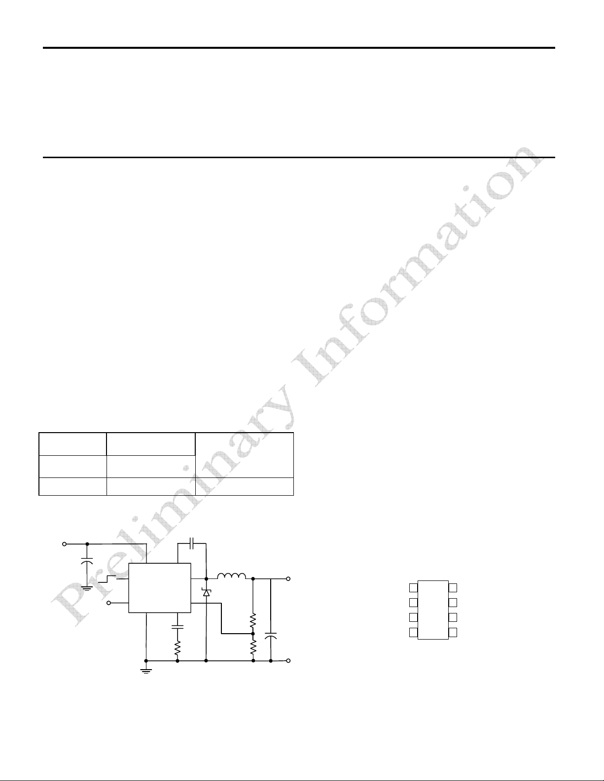
TYPICAL APPLICATION
PIN CONNECTIONS
INPUT
470µF/
10µF CER
ON
OFF
EN
SYNC
VIN
8
1
GND
AMS4155
5
BST
COMP
1µF
23
LX
4
F/B
6
7
10nF
5kΩ
Advanced Monolithic Systems, Inc.
B230A
10 µH
30kΩ
10kΩ
OUTPUT
5V/3A
40µF
ceramic
8L SOIC
SO Package (S)
8
EN
7
COMP
6
5FBGNDLX
SYNC
BST
VIN
1
2
3
4
Top View

http://www.BDTIC.com/AMS
PIN DESCRIPTION
Pin Number NAME DESCRIPTION
1 SYNC Synchronization Input. This pin is used to synchronize the internal oscillator frequency to
an external source. Leave SYNC unconnected or connect to GND if unused.
2 BST Bootstrap. This capacitor is needed to drive the power switch above the supply voltage. It
is connected between LX and BST pins to form a floating supply across the power switch
driver. The voltage across Cbst is about 5V and is supplied by the internal Vcc supply
when LX pin voltage is low.
3 VIN Supply Voltage. The AMS4155 operates from a+4.75V to +23V unregulated input. Cin is
needed to prevent large voltage spikes from appearing at the input power supply.
4 LX This connects the inductor to the internal Switch
5 GND Ground Pin connected to PCB ground plane. This pin is also the ground for internal voltage
reference.
6 FB Feedback. A resistor network of two resistors is used to set-up the output voltage connected
between Output to GND. The node between the two resistors is connected to Feedback pin.
AMS4155
7 COMP Compensation. This node is the output of the transconductance error amplifier and the
input to the current comparator. Frequency compensation is done at this node by
connecting a series R-C to ground.
8 ENABLE Enable. A voltage greater than 2.495V at this pin enables device operation.
Advanced Monolithic Systems, Inc.

http://www.BDTIC.com/AMS
AMS4155
ABSOLUTE MAXIMUM RATINGS
VIN 28V LX -1V to +28V
F/B -0.3V to +6V COMP -0.3V to +6V
EN -0.3V to +6V SYNC -0.3v to +6V
BST VLX + 6V
Junction Temperature
Storage Temperature
Lead temperature 1,6 mm (1/16 inch) from case for 10 seconds
ELECTRICAL CHARACTERISTICS
Electrical Characteristics at TA= 25 °C and VIN=12V (unless otherwise noted).
PARAMETER
Feedback Voltage 4.75V ≤ VIN≤ 20V, V
Switch On Resistance
Switch Leakage
Current Limit
Current Amplifier Gain
(1)
TEST CONDITIONS
< 2V 1.215 1.255 1.285 V
V
= 0V; VLX = 0V
EN
COMP
+150°C
-65°C to +150°C
260°C
AMS4155
Min. Typ. Max.
0.18 Ω
0 10 µA
3.4
4 6 A
1.9 A/V
Units
Error Amplifier Voltage Gain 400 V/V
∆I
= ± 10µA 730
Error Amplifier Transconductance
Oscillator Frequency
Sync Frequency Sync Drive 0.5V to 2.7V 0.460 1.1 MHz
Maximum Duty Cycle V
Minimum Duty Cycle VFB = 1.5V 3.2 %
Enable Threshold 2.2 2.475 2.55 V
Enable Hysteresis 220 mV
Enable Pull-up Current 0.7
Under Voltage Lockout
Threshold Rising
Under Voltage Lockout
Threshold Hysteresis
Supply Current (Shutdown) VEN ≤ 0.4V 17 25
Supply Current (Quiescent) V
Thermal Shutdown 153
Note:
1) Equivalent output current = 1.5A ≥ 50% Duty Cycle
2.0A ≤ 50% Duty Cycle
Assumes ripple current = 30% of load current.
C
= 1.0V 85 %
FB
≥ 2.8V; VFB = 1.5V 0.95 1.1 mA
EN
420 460 500 KHz
2.4
2.5
200
2.6
µA/V
µA
V
mV
µA
°C
Advanced Monolithic Systems, Inc.

http://www.BDTIC.com/AMS
TYPICAL PERFORMANCE CHARACTERISTICS
Light load start up
AMS4155
Full load start up
PWM rising edge
PWM Falling edge
Advanced Monolithic Systems, Inc.

http://www.BDTIC.com/AMS
TYPICAL PERFORMANCE CHARACTERISTICS (continued)
0.5-3A transient on 5V output
Typical waveform set at 3.3V output, 2A load and 12V input.
AMS4155
Full load Sat (reference = supply at IC)
Advanced Monolithic Systems, Inc.

http://www.BDTIC.com/AMS
PACKAGE DIMENSIONS inches (millimeters) unless otherwise noted.
8 LEAD SOIC PLASTIC PACKAGE (S)
0.189-0.197*
(4.801-5.004)
87 65
0.123 (3.12)
0.137 (3.48)
87 65
AMS4155
0.063(1.60)
0.228-0.244
(5.791-6.197)
0.053-0.069
(1.346-1.752)
0.014-0.019
(0.355-0.483)
12 34
0.138 (3.50)
0.050(1.27)0.024(0.61)
0.105(2.67)
0.050
(1.270)
TYP
0.150-0.157**
(3.810-3.988)
0.004-0.010
(0.101-0.254)
0.213(5.41)
0.090 (2.28)
0.102 (2.59)
12 34
0.010-0.020
(0.254-0.508)
0.008-0.010
(0.203-0.254)
0.016-0.050
(0.406-1.270)
*DIMENSION DOES NOT INCLUDE MOLD FLASH. MOLD FLASH
SHALL NOT EXCEED 0.006" (0.152mm) PER SIDE
**DIMENSION DOES NOT INCLUDE INTERLEAD FLASH. INTERLEAD
FLASH SHALL NOT EXCEED 0.010" (0.254mm) PER SIDE
x 45°
0°-8 ° TYP
S (SO- 8 ) AMS DRW# 0422 93
RECOMMENDED LAYOUT PATTERN
Advanced Monolithic Systems, Inc.
 Loading...