www.BDTIC.com/AMS
http://www.BDTIC.com/AMS
Advanced AMS4154
Monolithic 2A OUTPUT PWM BUCK CONVERTER
Systems
RoHS compliant
FEATURES APPLICATIONS
• Stable with low ESR Output Ceramic Capacitors • Battery Chargers
• Up to 99% On time • Portable (Notebook) Computers
• 2A Output Current • Industrial power supply
• Wide Operating Input Voltage Range 5.5V to 32V • Point of regulation for high performance electronics
• Fixed 330 kHz Frequency • Consumer Electronics
• Thermal Shutdown • Audio Power Amplifiers
• Cycle-by-cycle Over Current Protection • Distributed Power Systems
• Under Voltage Lockout • Pre-Regulator for Linear Regulators
• 5V reference output • LCD TVs and LCD monitors
• Adjustable output from 0.6V • Automotive electronics
GENERAL DESCRIPTION
The AMS4154 is a 2A step-down converter for high voltage applications. Current mode operation provides easier compensation
and fast transient response. Internal cycle-by-cycle current limiting and thermal shutdown provides the necessary protection in
faults situation. A 5V reference voltage is available that can supply up to 2mA current. Available in 8-pin SOIC EDP package.
ORDERING INFORMATION
OUTPUT PACKAGE TYPE TEMP. RANGE
VOLTAGE 8 Lead SOIC EDP
Adjustable AMS4154S -25°C to 125°C
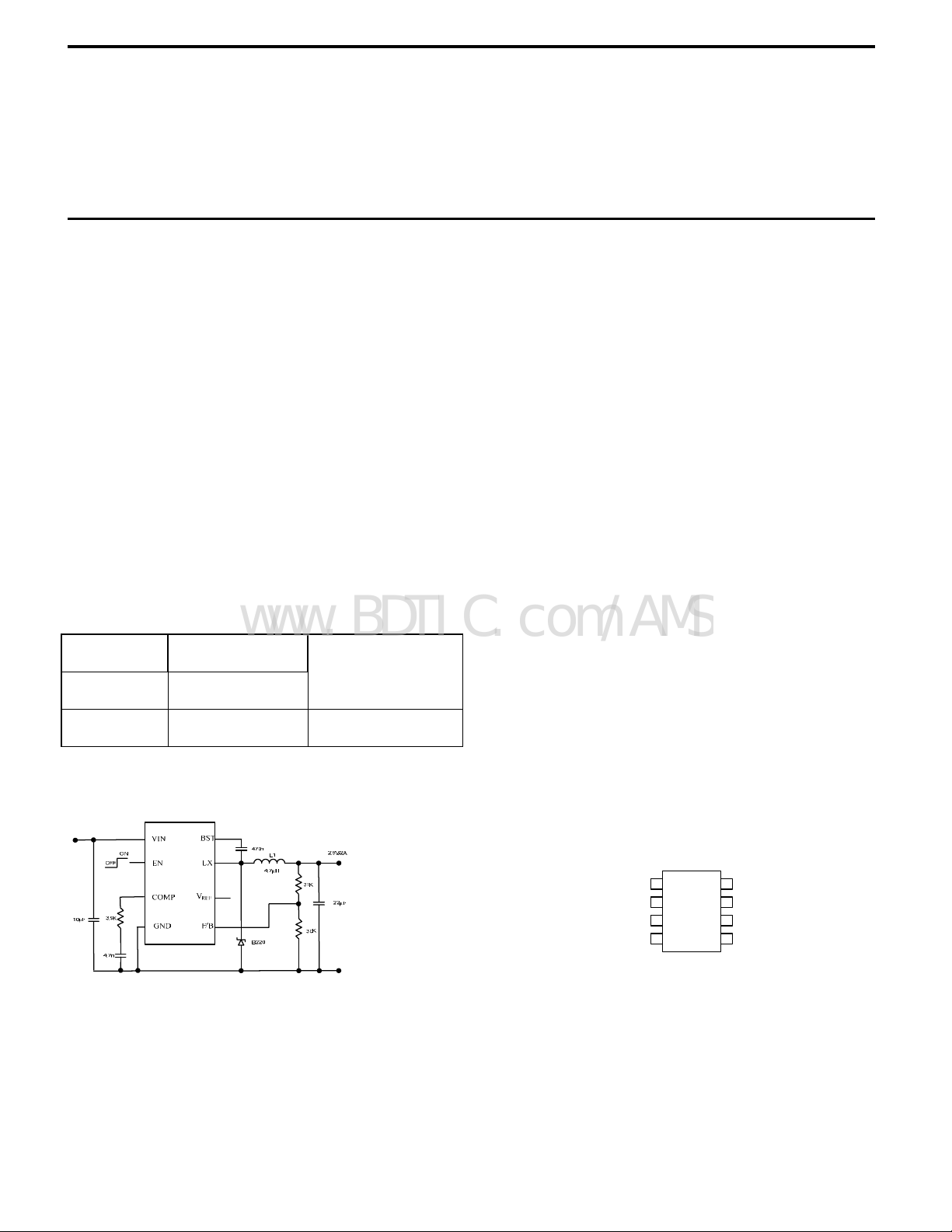
TYPICAL APPLICATION
PIN CONNECTIONS
8L SOIC
SO Package (S)
BST
VIN
LX
GND
1
2
3
4
8
7
6
5
REF
EN
COMP
F/B
Advanced Monolithic Systems, Inc.
Top View
Paddle is GND

www.BDTIC.com/AMS
http://www.BDTIC.com/AMS
PIN DESCRIPTION
AMS4154
AMS4154
PIN
NUMBERS
1 BST Bootstrap. A capacitor is needed to drive the power switch’s drive above the supply
2 VIN Supply Voltage. The AMS4154 operates from a+5.5V to +32V unregulated input. C1 is
3 LX Switch. This connects the inductor to VIN through the internal power switch.
4 GND Ground. This pin is the ground for voltage reference and for the regulated output voltage.
5 FB Feedback. An external resistor divider from the output to GND, tapped to the FB pin sets
6 COMP Compensation. This node is the output of the transconductance error amplifier and the
7 EN Enable. A voltage greater than 2.5V enables operation. For complete low current shutdown
8 REF 5V reference voltage capable of supplying 1mA for other external circuits.
NAME DESCRIPTION
voltage. It is connected between LX and BST pins to form a floating supply across the
power switch driver.
needed to prevent large voltage spikes from appearing at the input.
For this reason care must be taken in its layout.
the output voltage.
input to the current comparator. Frequency compensation is done at this node by
connecting a series R-C to ground.
the EN pin voltage needs to be less than 2.3V.
Advanced Monolithic Systems, Inc.

www.BDTIC.com/AMS
http://www.BDTIC.com/AMS
AMS4154
ABSOLUTE MAXIMUM RATINGS
Input Supply Voltage -0.3V to +34V Junction Temperature
SW Voltage -1V to VIN + 0.3V Storage Temperature
BS Voltage V LX – 0.3V to V LX + 6V Lead Temperature
All Other Pins -0.3V to +6V
-65°C to +150°C
ELECTRICAL CHARACTERISTICS
Electrical Characteristics at TA= 25 °C and VIN=12V (unless otherwise noted).
PARAMETER
Feedback Voltage
Supply Current
Shutdown Supply Current VEN = 0V 0.5 1 µA
Current Limit
Current Sense to COMP
Transconductance
TEST CONDITIONS
12V ≤ V
V
EN
≤ 32V, V
IN
= 2.6 V, VFB = 1.4V
AMS4154
< 2V 1.202 1.230 1.258 V
COMP
Min. Typ. Max.
2.0 3.5 mA
2.5 3.6 3.9 A
5.0 A/V
+150°C
260°C
Units
Oscillation Frequency 280 330 380 KHz
V
= 1.0V
Maximum Duty Cycle
Minimum Duty Cycle VFB = 1.5V 0 %
EN Threshold Voltage VEN Rising, Output ON
EN Threshold Voltage V
EN Threshold Hysteresis 100 mV
Enable Current VEN = 0V 1.8 µA
Thermal Shutdown 160 ºC
5V REF Voltage I
REF Load Regulation ∆I
REF Line Regulation I
FB
Falling , Output OFF 2.2 2.3 V
EN
= 0 4.8 5.0 5.2 V
REF
= 0 to 1mA 50 mV
REF
= 100µA, VIN = 6.5 to 32V 30 mV
REF
90 99 %
2.5 2.6 2.8 V
Advanced Monolithic Systems, Inc.

www.BDTIC.com/AMS
http://www.BDTIC.com/AMS
TYPICAL APPLICATION
AMS4154
12Input to 5v Output
VIN
F/B GND
COMP
on
off
C5
+
470µ
C6
22n
R3
1K
EN
REF BST
C7
100n
LX
VIN
24 Input to 3.3VOutput @2A
100n
22µH
L1
C1
220n
C1
D1
B220
R2
3K
R1
1K
C3
10µ
3.3V
+
V
OUT
C4
68µ
Advanced Monolithic Systems, Inc.

www.BDTIC.com/AMS
http://www.BDTIC.com/AMS
TYPICAL PERFORMANCE
AMS4154
Advanced Monolithic Systems, Inc.

AMS4154
www.BDTIC.com/AMS
http://www.BDTIC.com/AMS
TYPICAL PERFORMANCE
Output Variation due to Supply (1A Load) Reference Output Load Regulation
300
200
100
0
0 5 10 15 20 25 30
-100
-200
-300
-400
Voltage Coefficient PPM
Efficiency for 5V Output with 12V Input Switching Output at 1A
90
88
86
84
%
82
80
78
76
0.5 1 1.5 2 2.5 3
Efficiency
Int Diode Ext Diode Ext Diode 22uH
Load A
Start Up into 1A resistive Load Output Stop into 1A resistive Load
Advanced Monolithic Systems, Inc.
0
-0.5
-1
%
-1.5
-2
-2.5
0 0.001 0.002 0.003 0.004 0.005

www.BDTIC.com/AMS
http://www.BDTIC.com/AMS
AMS4154
TYPICAL PERFORMANCE (continued)
Rise Time at Switching node and 1A Load Fall Time at Switching node and 1A Load
Load Transient response 0.5-2.5A 1µS Rise/Fall Time Load Transient 1.5-1.5A 1µS Rise/Fall Time
Compensation 4.7k/4.7n Compensation 1.7k/4.7n
No Load Waveform Output Ripple as 3A for 5V Output 2x 10µF ceramic
Output and 10µH inductor
Advanced Monolithic Systems, Inc.

www.BDTIC.com/AMS
http://www.BDTIC.com/AMS
PACKAGE DIMENSIONS inches (millimeters) unless otherwise noted.
8 LEAD SOIC PLASTIC PACKAGE (S)
0.189-0.197*
(4.801-5.004)
87 65
0.123 (3.12)
0.137 (3.48)
87 65
AMS4154
0.063(1.60)
0.228-0.244
(5.791-6.197)
0.053-0.069
(1.346-1.752)
0.014-0.019
(0.355-0.483)
12 34
0.138 (3.50)
0.050(1.27)0.024(0.61)
0.105(2.67)
0.050
(1.270)
TYP
0.150-0.157**
(3.810-3.988)
0.004-0.010
(0.101-0.254)
0.213(5.41)
0.090 (2.28)
0.102 (2.59)
12 34
0.010-0.020
(0.254-0.508)
0.008-0.010
(0.203-0.254)
0.016-0.050
(0.406-1.270)
*DIMENSION DOES NOT INCLUDE MOLD FLASH. MOLD FLASH
SHALL NOT EXCEED 0.006" (0.152mm) PER SIDE
**DIMENSION DOES NOT INCLUDE INTERLEAD FLASH. INTERLEAD
FLASH SHALL NOT EXCEED 0.010" (0.254mm) PER SIDE
x 45°
0°-8 ° TYP
S (SO- 8 ) AMS DRW# 0422 93
RECOMMENDED LAYOUT PATTERN
Advanced Monolithic Systems, Inc.
 Loading...