

http://www.BDTIC.com/AMS
Advanced AMS4106
Monolithic 5A SYNCHRONUS PWM BUCK CONVERTER
Systems
RoHS compliant
FEATURES APPLICATIONS
• Internal MOSFET driver with Integrated High Side • LCD TVs and LCD monitors
• Uses External Low Side MOSFET • Computer Peripherals
• Adjustable output voltage dawn to 0.600V • Portable (Notebook) Computers
• External Clock Synchronization • Industrial power supply
• Built in Start/Stop UVLO • Point of regulation for high performance electronics
• Over Current and Thermal Protection • Consumer Electronics
• Shutdown supply current < 1uA • Audio Power Amplifiers
• Frequency range 100KHz to 750KHz
GENERAL DESCRIPTION
The AMS4106 is a medium output current synchronous buck converter. The high side device is integrated into the device. The
AMS4106 provides an adaptive gate drive for the extern al FET. For low current operation this can be replaced with a Schottk y
diode allowing asynchronous operation. The part has either a fixed internal present PWM frequency of 250 kHz, or externally
adjustable up to 600 kHz, allowing smaller inductors where efficiency is less critical and faster transient response is needed.
The part uses current mode control for simple compensation and ease of use with low ESR capacitors. It uses a programmable
soft start to reduce inrush current and allow large output capacitors to be used where very low ripple is required. The part has
enable pin with virtual zero power in shutdown mode. A power good is provided with open collector to facilitate power ready
functions. The part is available in SOIC 16 thermally enhanced packages.
ORDERING INFORMATION
OUTPUT PACKAGE TYPE TEMP.
VOLTAGE 16 Lead SOIC RANGE
Adjustable AMS4106S -25ºC to 125ºC
TYPICAL APPLICATION PIN CONNECTIONS
Advanced Monolithic Systems, Inc.
16 Lead SOIC
(S)
1
PWRGD
2
SS
3
GND
4
VPWR
VPWR
5
V
IN
6
COMP
7
F/B
8
16
15
1314LX
12
11
10
9
FDR
PGND
LX
LX
BST
ENABLE
F SET
Top View

http://www.BDTIC.com/AMS
PIN DESCRIPTION
AMS4106
AMS4106
PIN
NUMBERS
1 PWRGD Power good output. Open collector output. A low on the pin indicates that the output is less
2 SS Soft start pin connect a capacitor to GND, to slow the start up.
3 GND Analog ground-internally connected to the sensitive analog ground circuitry.
4, 5 VPWR Input supply voltage, 4.5 V to 20 V. Must bypass with a low ESR 10–µF ceramic capacitor.
6 VIN Input supply voltage, 4.5 V to 20 V powers up the internal circuitry. Must bypass with a
7 COMP Error amplifier outpu t. Connect frequency compensation network from COMP to GND.
8 F/B Input pin of the error comparator.
9 F SET External frequency set 100 Khz-750Khz.
10 ENABLE Logic enable/disable device function.
11 BST Boost voltage for the output stage drive. Connect a capacitor between LX pin and Boost.
12, 13, 14 LX Phase node- Connect to external FET and external L-C filter.
15 PGND Power Ground-No isy internal ground-Return currents from the FDR driver output return
NAME DESCRIPTION
than the desired output voltage. There is an internal rising filter on the output of the
PWRGD comparator.
low ESR 10–
through the PGND
µF ceramic capacitor.
16 FDR Gate drive for low side MOSFET. Connect gate of n-channel MOSFET.
Advanced Monolithic Systems, Inc.

http://www.BDTIC.com/AMS
AMS4106
ABSOLUTE MAXIMUM RATINGS
VIN -0.3V to 30V LX Internally Limited
F/B -0.3 to 8.0V FDR (steady state current) 500 mA
EN -0.3V to 8.0V COMP 3 mA
FSET -0.3V to 4.0V FDR (steady state current) 100 mA
SS -0.3V to 4.0V LX (steady state current) 500 mA
BST VI (PH) + 8.0V COMP 3 mA
FDR -0.3V to 8.5V SS PWRGD 10 mA
PWRGD 0.3V to 30V AGND to PGND ±0.3V
COMP 0.3V to 30V ESD 2kV
LX -1.5V to 30V Junction Temperature +150°C
Lead Temperature1,6 mm for 10 sec. 260°C Storage Temperature -65°C to +150°C
Stresses beyond those listed under absolute maximum ratings may cause permanent d a mage to the device. These are stress ratings
only, and functional operation of the device at these or any other conditions beyond those in dicated under recommended operating
conditions is not implied. Exposure to absolute-maximum-rated conditions for extended periods may affect device reliability.
ELECTRICAL CHARACTERISTICS
Electrical Characteristics at TJ = 25 °C and Vin=12V (unless otherwise noted)
PARAMETER
SUPPLY CURRENT
Quiescent current
I
Q
VIN
Start threshold voltage
Stop threshold voltage
Hysteresis
TEST CONDITIONS
Operating Current, LX pin open,
No external low side MOSFET,
Shutdown, EN= 0V
Min. Typ. Max.
3.69 3.97 V
AMS4106
3 12 mA
0.5
4.32 4.49 V
350 mV
Units
µA
REFERENCE SYSTEM ACCURACY
Reference voltage
OSCILLATOR (RT PIN)
Internally set PWM switching
frequency
ERROR AMPLIFIER F/B and COMP PINS
Error amplifier Sink current
Running
Error amplifier Source current
Running
Error amplifier Source current
Start-up
Advanced Monolithic Systems, Inc.
TJ = 25 oC 0.588
T
= 125 oC
J
F set open
F set to GND
F set to VCC
0.600 0.612 V
0.600 V
200 250 300
kHz
60 85
1.0 98
20
kHz
µA
µA
µA

http://www.BDTIC.com/AMS
AMS4106
ELECTRICAL CHARACTERISTICS (continued)
Electrical Characteristics at TJ = -40 °C to 125 °C and Vin = 4.5V (unless otherwise noted)
PARAMETER
Soft Start (SS) 2.22
POWER GOOD (PWRGD PIN)
Power good threshold Rising voltage
PWR
GD
Output saturation voltage
Output saturation voltage
Open collector leakage Voltage on PWRGD = 6 V
CURRENT LIMIT
Current limit VIN = 12 6.1 6.5 7.5 A
Current limit Hiccup Time f = 500 kHz 4.5 ms
THERMAL SHUTDOWN
Thermal shutdown trip point 145
Thermal shutdown hysteresis
LOW SIDE EXTERNAL FET DRIVE
Turn on rise time, (10%/90%)
Deadtime
(1)
(1)
(1)
OUTPUT POWER MOSFETS (LX PIN)
Lx node voltage when disabled DC conditions and no load, EN = 0 V 0.5 V
diode
r
High side power switch
DS (ON)
(1) Specified by design, not production tested.
Advanced Monolithic Systems, Inc.
f
= 250 kHz 4.6 Internal soft start (10% to 90%)
= 500 kHz
f
TEST CONDITIONS
Min. Typ. Max.
f = 250 kHz
= 500 kHz
f
= 1 mA, VIN > 4.5 V
I
sink
= 1 µA, VIN = 0 V
I
sink
VIN = 4.5V, Capacitive load = 1000 pF 15
10
AMS4106
2.3
95%
4 Rising edge delay
2
0.05 V
0.075 V
2
VIN = 8 V, Capacitive load = 1000 pF 12
VIN = 12 V 60 ns
VIN = 4.5 V sink/ source 7.5 Driver ON resistance
VIN = 12 V sink/ source 5
VIN = 4.5 V, Idc = 100 mA 1.13 1.42 Voltage drop, low side FET and
VIN = 12 V, Idc = 100 mA 1.08 1.38
VIN = 4.5 V, BST-LX = 4.5 V, Io = 0.5 A
VIN = 12 V, BST-LX = 8 V, I
o =
0.5 A
60
40 m
Units
µA
ms
ms
µA
°C
°C
ns
Ω
V
Ω

http://www.BDTIC.com/AMS
TYPICAL PERFORMANCE CHARACTERISTICS
87
86
85
84
%
83
82
81
80
79
0246
0.602
0.6015
0.601
0.6005
0.6
0.5995
0.599
Feedback Voltage
0.5985
0.598
5 7 9 1113151719
Advanced Monolithic Systems, Inc.
250Khz 3.3v output effici ency
Amps
Line Regulati on
Supply
270
268
266
264
262
260
258
Frequency
256
254
252
250
12v Efficiency
18v Efficiency
Series1
Frequency Stability
5101520
Supply voltage
AMS4106
5v output effici ency
0.88
0.87
0.86
0.85
0.84
0.83
0.82
0.81
0.8
0.79
0123456
output current
Load Rulation
0.61
0.605
0.6
0.595
Feedback voltag e
0.59
0123456
Amps
Series1
12v eff
18v Eeff
Series1

http://www.BDTIC.com/AMS
AMS4106
TYPICAL PERFORMANCE CHARACTERISTICS (continued)
FIG.1 FIG.2
Normal operating waveform, with internal frequency, Power good threshold ~95%, 2.5A load start up.
12V input and 2A load.
FIG.3 FIG.4
Power good at Light load Start up <10mA Shutdown
FIG.5 FIG.6
Trailing Edge Non Overlap Leading Edge Non Overlap
Advanced Monolithic Systems, Inc.

http://www.BDTIC.com/AMS
AMS4106
TYPICAL PERFORMANCE CHARACTERISTICS (continued)
FIG.7 FIG.8
Load Transient test performance 0.5A to 4A/10 µs Supply current through transient event (0.5-4A)
Scale 100mV division, Current/ fall time 10 µs Current scale is 0.5A per division
FIG. 9 FIG. 10
Output Ripple at 3A Load Supply ripple current at 4A (200mA per divi si on)
FIG. 11 FIG. 12
Start up current with 2A load Input Current during start up and shutdown.
Current is 200mA per division.
Advanced Monolithic Systems, Inc.

http://www.BDTIC.com/AMS
AMS4106
DETAIL DESCRIPTION and GUIDELINES
Start up from enable
When the enable is low the part is completely shut down with the nano-amps only of leakage current. When the enable is taken
above the turn on threshold it powers up part. There are 2 soft start mechanisms in operation during start up, error amplifier and
external. For small output capacitance (ceramic only solutions), the compensation can be used for soft start, and the soft start pin
is left open. For situation requiring slower soft start or where large output capacitors are used a separate soft start pin is used.
This charges the external capacitor with around 2.2 µA current allowing small ceramic capacitors to be used. When Power good
senses the output is almost at its final value the error amplifier current is turned on to its normal running current overriding the
startup current.
Enable connected to Vin
The part initiates its soft start described above at UVLO threshold of around 4.75V.
PWM frequency
The default it internally set to 250 kHz with the FSET pin left open. Adding a resistor to ground switches it into the external set
mode. A 68K resistor to ground gives approximately 250 kHz PWM frequency. Care should be taken to keep the resistor close
to the part as pick-up on this pin can cause jitter.
Over-current shutdown
If over-current is sensed the part shuts down and initiates the soft start sequence providing a hiccup function. This means that
shorting the output is non destructive and will run a low supply current. When the output shuts down the low-side FET is turned
off giving a tri-state output. This helps prevent negative output voltages being generated in an overload condition where the load
significantly reduces (due to system reset etc) as a result of the output voltage failing. Power good is held low during over
current.
Synchronous operation
With an external FET fitted between Phase and ground the parts enters synchronous operation. Gate time is adaptively
controlled allowing large freedom in the choice of output FET. For highest performance the lowest gate charge FET typically
will give the best overall efficiency. The gate drive features a medium drive capability of around 0.5-1A removing the need
series gate resistors for most applications. Due to the fast switching on the phase node it is important that the FET is placed very
close to the part with very short paths for both ground and the phase node. Large parasitic inductance can cause large negative
spikes on the switch output causing jitter and in severe circumstances potential circuit malfunction.
Asynchronous operation
A Schotty diode can be used in place of the FET for certain applications, no other changes are required to accommodate this
mode. The gate drive pin should be left open. This is at the expense of full load efficiency especially at low output voltage.
Transient performance is also reduced.
For applications when light load higher efficiency is required Asynchronous operation is preferred.
For Applications requiring HOT switching Asy nc hr o no us operation is preferred preventing unwant ed di ps on the output supply.
Duty cycle considerations
For low input output ratios greater than 50% duty cycle the maximum output should be de-rated to reduce package heating and
thermal shutdown.
For high input output ratios the maximum frequency is determined by the minimum useable duty cycle, for this part it is around
120ns, shorter duty cycles could cause jitter or pulse skipping. For a 0.8v output and a switching frequency of 500kHz a
maximum input voltage of around 14v can be accommodated at light load rising to about 20v at 4A.
Bootstrap Circuit
To allow operation over a very large range the devices uses an internal boost regulator and internal boost diode. The boost
capacitor supplies the output bias current requirements. The regulator is set to the minimum voltage required to give operation at
full output current. It is important that the capacitor is large enough to supply the cu rrent for the full on time for large duty 1µF
is recommended for short duty cycle<10% 100nf is suitable. Using a 1µF boost capacitor for all applications has no detrimental
effect. The voltage across the capacitor is small (around 3v) so small ceramic case sizes can be used.
Advanced Monolithic Systems, Inc.

http://www.BDTIC.com/AMS
AMS4106
DETAIL DESCRIPTION and GUIDELINES (continued)
Reference Circuit
A high precision bandgap is used giving a low TC and good supply rejection. The output is attenuated to give a reference
voltage of 0.600V making it suitable for very low output voltage applications.
COMPENSATION
The converter is of the current mode topology considered simplifying the selection of compensation components. For most
voltages this simple formula is a good starting point
Ccomp = 15e-9/Vout for L = 10e-6 and Cout = 44e-6
Ccomp is proportional to the output inductors and output capacitor
Rcomp = 18e3/Vout
Output capacitor Cout, is a function of the maximum current and ripple required.
Multiple capacitors may be required to give the optimum ripple and transient response.
The stability is not that critical for varying Cout, however to prevent OCP during fast load transients Ccomp, h a s to be increased
in proportion to Cout.
The current gain of the output stage is approximately 6A/volt
The running transconductance output current is
Sourcing current 95 µA
Sinking current 85 µA
This equates to about 600e-6 mohs
For best transient response each application is unique and these components should only be used as a starting point.
Advanced Monolithic Systems, Inc.

http://www.BDTIC.com/AMS
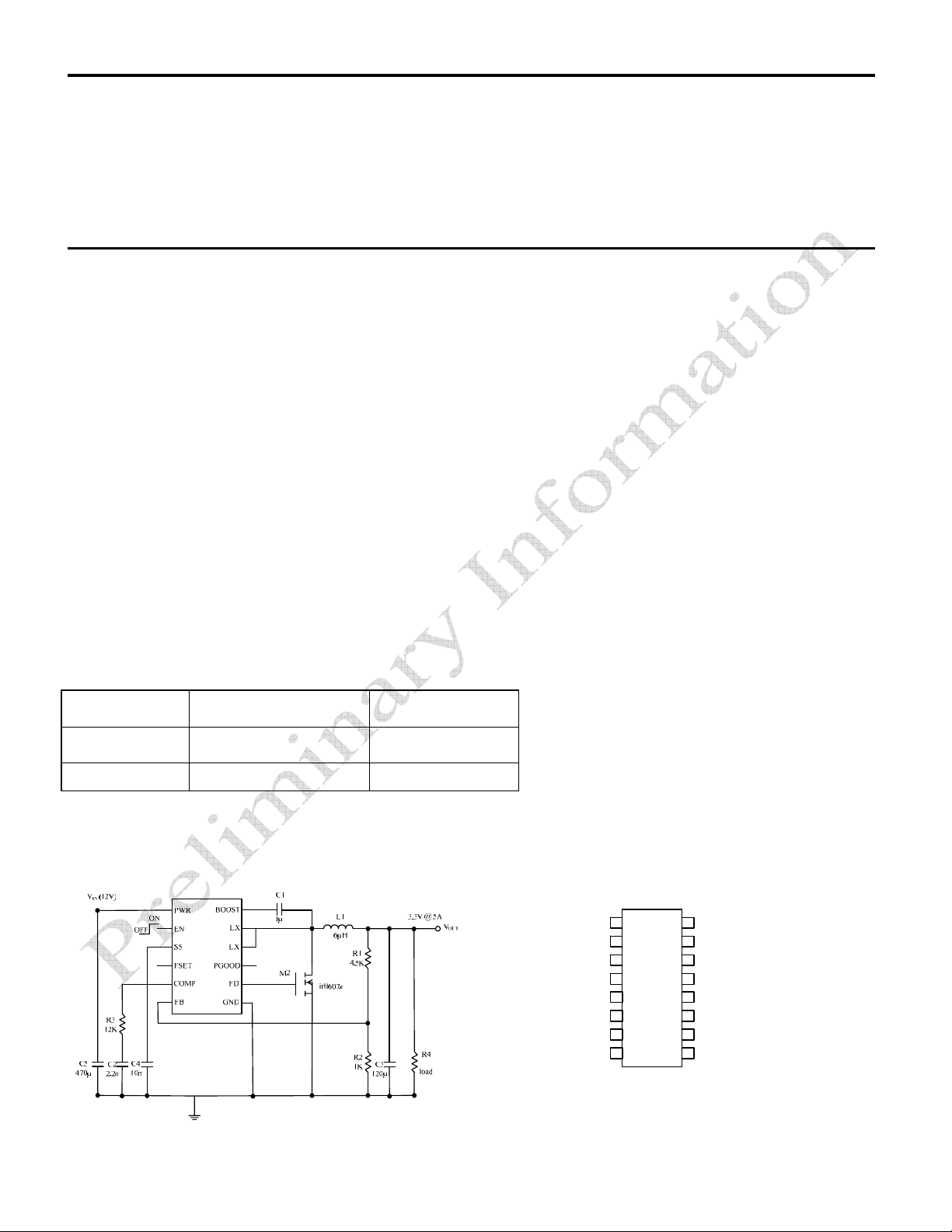
APPLICATION EXAMPLE
AMS4106
TESTING CONDITION FOR ABOVE CIRCUIT
Supply Working range 6-20V Maximum 5A input voltage @23V
Gate drive voltage max 8V Nominal frequency 258 kHz
Gate and output wave form.
Small kick on gate drive present at 20V in 5V/4A output
Advanced Monolithic Systems, Inc.

http://www.BDTIC.com/AMS
PACKAGE DIMENSIONS inches (millimeters) unless otherwise noted.
16 LEAD SOIC PACKAGE (S)
0.386-0.393*
(9.80-10.0)
AMS4106
0.228-0.244
(5.791-6.197)
0.053-0.069
(1.346-1.752)
0.013-0.020
(0.33-0.51)
*DIMENSION DOES NOT INCLUDE MOLD FLASH. MOLD FLASH
SHALL NOT EXCEED 0.006" (0.152mm) PER SIDE
**DIMENSION DOES NOT INCLUDE INTERLEAD FLASH. INTERLEAD
FLASH SHALL NOT EXCEED 0.010" (0.254mm) PER SIDE
0.050
(1.270)
TYP
0.150-0.157**
(3.810-3.988)
0.004-0.010
(0.101-0.254)
0.008-0.010
(0.203-0.254)
0.010-0.020
(0.254-0.508)
0.016-0.050
(0.406-1.270)
x 45°
0°-8° TYP
S (SO-16 ) AMS DRW# 0702021
Advanced Monolithic Systems, Inc.
 Loading...