

ROHM US6K1 Schematic [ru]
C
T
2.5V Drive Nch+Nch MOSFET
US6K1
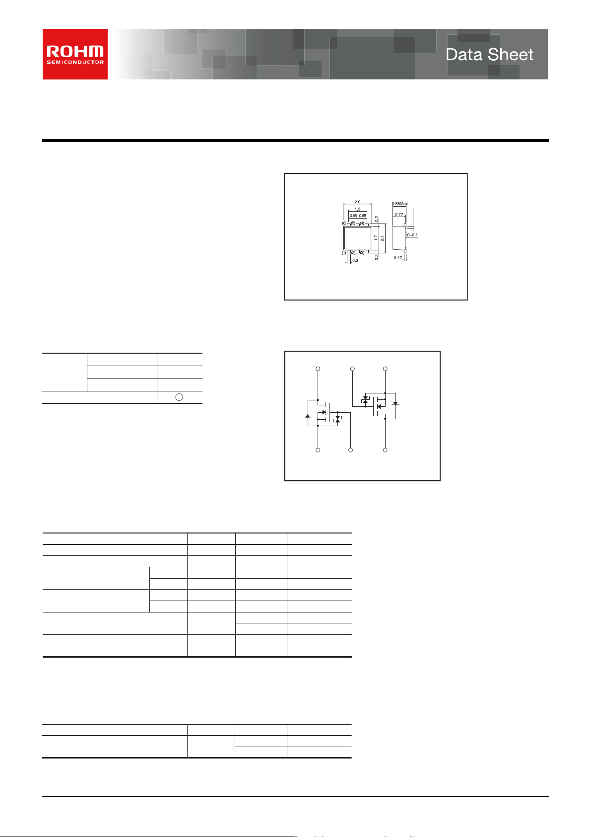
zStructure zDimensions (Unit : mm)
Silicon N-channel MOSFET
zFeatures
1) Low On-resistance.
2) Space savingsmall surface mount package (TUMT6).
3) Low voltage drive (2.5V drive).
zApplications
Switching
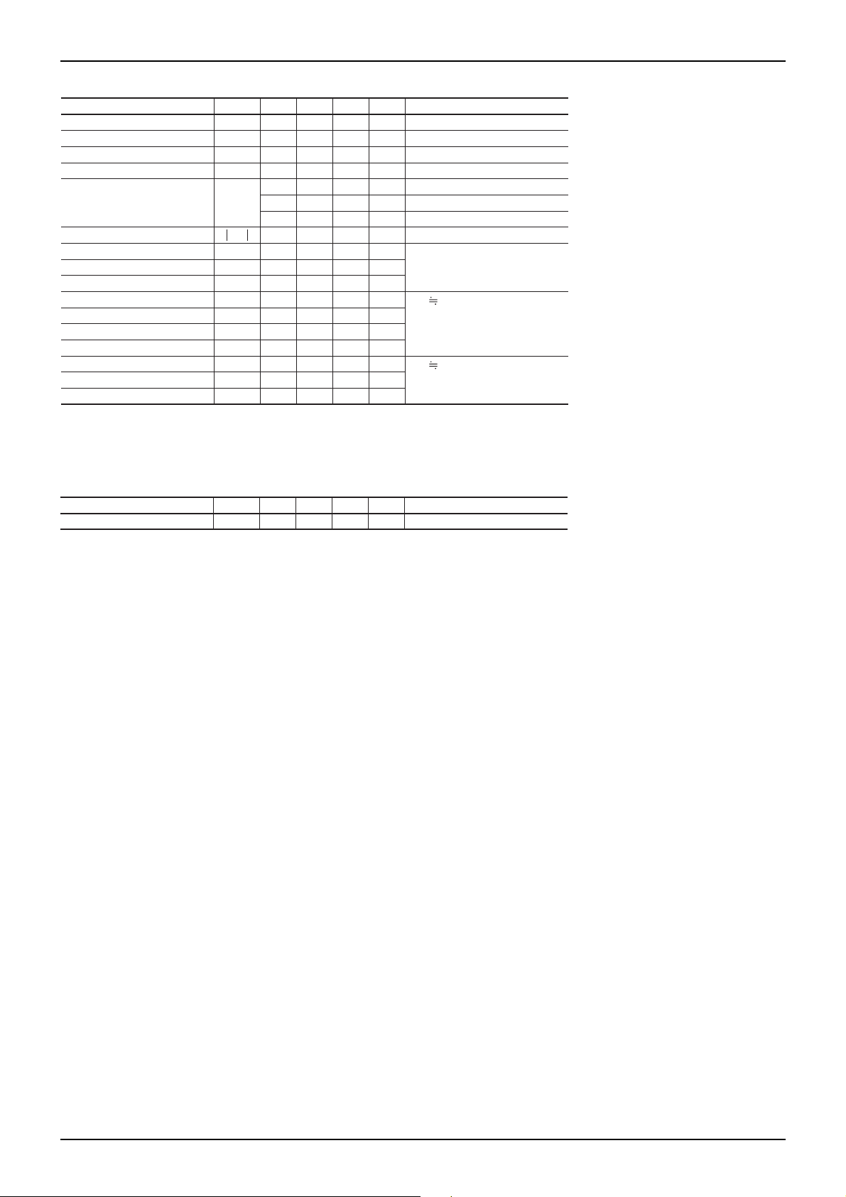
zPackaging specifications zInner circuit
TUMT6
0.2Max.
Abbreviated symbol : K01
Type
Package
Code
Basic ordering unit (pieces)
Taping
TR
3000
US6K1
zAbsolute maximum ratings (Ta=25°C)
Parameter
Drain-source voltage
Gate-source voltage
Drain current
Source current
(Body diode)
Total power dissipation
Channel temperature
Range of storage temperature
∗1 Pw≤10µs, Duty cycle≤1%
∗2 Mounted on a ceramic board
Continuous
Pulsed
Continuous
Pulsed
Symbol
zThermal resistance
Parameter
hannel to ambient
∗ Mounted on a ceramic board
Symbol Limits Unit
Rth(ch-a)
(6)
(5)
∗2
∗1
(1)
∗1 ESD PROTECTION DIODE
∗2 BODY DIODE
(2)
(4)
∗1
∗2
(1) Tr1 Source
(2) Tr1 Gate
(3) Tr2 Drain
(3)
(4) Tr2 Source
(5) Tr2 Gate
(6) Tr1 Drain
Limits Unit
P
DSS
GSS
D
DP
S
SP
D
∗1
∗1
∗2
30
12
±1.5
±6
0.6
6
1.0
150
−55 to +150
VV
VV
AI
AI
AI
AI
W / TOTAL
W / ELEMENT0.7
°CTch
°CTstg
125
∗
179
°C/W / TOTAL
°C/W / ELEMEN
www.rohm.com
c
○
2009 ROHM Co., Ltd. All rights reserved.
1/3
2009.03 - Rev.B
US6K1
zElectrical characteristics (Ta=25°C)
Parameter Symbol
Gate-source leakage
Drain-source breakdown voltage
V
(BR) DSS
Zero gate voltage drain current
Gate threshold voltage
Static drain-source on-state
resistance
V
R
Forward transfer admittance
Input capacitance
Output capacitance
Reverse transfer capacitance
Turn-on delay time
Rise time
Turn-off delay time
Fall time
Total gate charge
Gate-source charge
Gate-drain charge
∗Pulsed
zBody diode characteristics (Source-drain) (Ta=25°C)
Parameter Symbol
I
GSS
I
DSS
GS (th)
DS (on)
Y
fs
C
iss
C
oss
C
rss
t
d (on)
t
r
t
d (off)
t
f
Q
Q
gs
Q
gd
V
SD
∗
∗
∗
∗
∗
∗
∗
g
∗
∗
Min.−Typ. Max.
Unit
Conditions
− 10 µAVGS=12V, VDS=0V
30 −−VID= 1mA, VGS=0V
−−1 µAV
0.5 − 1.5 V V
− 170 240 I
mΩ
− 180 250 mΩ
− 240 340 I
mΩ
1.5 −−SV
− 80 − pF V
− 1312− pF V
−
−
−
−
−
−
−
−−nC I
Min. Typ. Max.
− pF f=1MHz
7
− ns
9
− ns
15
− ns
6
− ns
1.6
2.2 nC
0.5
− nC V
0.3
Unit
= 30V, VGS=0V
DS
= 10V, ID= 1mA
DS
= 1.5A, VGS= 4.5V
D
= 1.5A, VGS= 4.0V
I
D
= 1.5A, VGS= 2.5V
D
= 10V, ID= 1.5A
DS
= 10V
DS
=0V
GS
VDD 15V
ID= 0.75A
GS
= 4.5V
V
L
= 20Ω
R
G
=10Ω
R
15V
V
DD
= 4.5V
GS
= 1.5A
D
Conditions
−−1.2 V IS= 0.6A, VGS=0VForward voltage
Data Sheet
www.rohm.com
c
○
2009 ROHM Co., Ltd. All rights reserved.
2/3
2009.03 - Rev.B
 Loading...