

Transistors
2.5V Drive Nch+Nch MOS FET
UM5K1N
zStructure
Silicon N-channel MOS FET
zFeatures
1) Tw o 2SK3018 transistors in a single UMT package.
2) Mounting cost and area can be cut in half.
3) Low on-resistance.
4) Low voltage drive (2.5V) makes this device ideal for
portable equipment.
5) Drive circuits can be simple.
zApplica tions
Interfacing, switching (30V, 100mA)
zPackaging specifications zEquivalent circui
Type
UM5K1N
Package
Code
Basic ordering unit
(pieces)
Taping
TR
3000
zAbsolute maximum ratings (Ta=25°C)
<It is the same ratings for Tr1 and T r2.>
Parameter
Drain-source voltage
Gate-source voltage
Drain current
Total power dissipation
Channel temperature
Storage temperature
1 Pw≤10µs, Duty cycle≤50%
∗
2 With each pin mounted on the recommended lands.
∗
Continuous
Pulsed
Symbol
DSS
V
V
GSS
D
I
I
DP
∗
P
D
Tch
Tstg
∗
1
2
Limits Unit
30
±20
±100
±400
150
150
−55 to +150
zThermal resistance
Parameter
Channel to ambient
∗ With each pin mounted on the recommended lands.
Symbol Limits Unit
Rth(ch-a)
∗
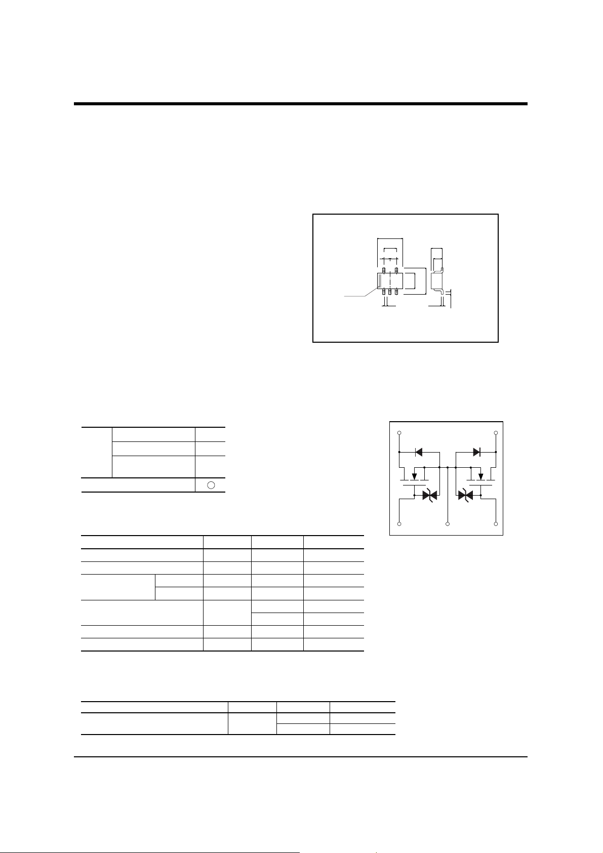
zExternal dimensions (Unit : mm)
UMT5
2.0
1.3
0.65
0.65
(5)
(4)
(1)
(2)
1pin mark
(3)
0.2
Abbreviated symbol : K1
Tr1 Tr2
(1)
(1) Tr1 Gate
(2) Source
V
V
mA
mA
mW / TOTAL
mW / ELEMENT120
˚C
˚C
(3) Tr2 Gate
(4) Tr2 Drain
(6) Tr1 Drain
833
1042
°C / W / TOTAL
°C / W / ELEMENT
1.25
Each lead has same dimensions
∗
Gate
Protection
Diode
UM5K1N
0.9
0.7
2.1
0.15
0.1Min.
(4)(6)
∗
Gate
Protection
Diode
(2) (3)
A protection diode has been built in between
∗
the gate and the source to protect against
static electricity when the product is in use.
Use the protection circuit when rated
voltagesare exceeded.
Rev.A 1/3
Transistors
zElectrical characteristics (Ta=25°C)
<It is the same characteristics for Tr1 and T r2.>
Parameter Symbol
Gate-source leakage
Drain-source breakdown voltage
Zero gate voltage drain curren
Gate threshold voltage
Static drain-source on-stage
resistance
Forward transfer admittance
Input capacitance
Output capacitance
Reverse transfer capacitance
Turn-on delay time
Rise time
Turn-off delay time
Fall time
I
V
(BR)DSS
I
t
V
R
R
C
C
t
t
GSS
DSS
GS(th)
DS(on)
DS(on)
Y
fs
C
iss
oss
rss
d(on)
r
t
d(off)
f
t
Min.
−
30
−
0.8
−
− 713
20
−
−
−
− 15 − ID=10mA, V
− 35 − V
− 80 − RL=500Ωns
− 80 − RG=10Ωns
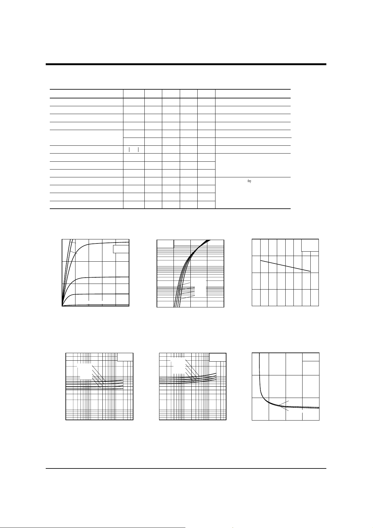
zElectrical characteristic curves
0.15
A)
D (
0.1
0.05
DRAIN CURRENT : I
4V
3V
3.5V
2.5V
2V
0
012345
DRAIN-SOURCE VOLTAGE : V
VGS=1.5V
Ta=25˚C
Pulsed
DS (
Fig.1 Typical output characteristics
V)
200m
100m
50m
A)
(
D
20m
10m
5m
2m
1m
0.5m
DRAIN CURRENT : I
0.2m
0.1m
Fig.2 Typical transfer characteristics
50
Ta=125˚C
20
(on) (Ω)
DS
10
5
75˚C
25˚C
−25˚C
V
GS=4V
Pulsed
(on) (Ω)
DS
Typ. Max. Unit Test Conditions
µAV
±1
−
−
−
1
−
1.5
−
8
5
−
−
9
4
1
Ta=125˚C
75˚C
25˚C
−25˚C
−
−
−
Ta=125˚C
2
75˚C
25˚C
−25˚C
13
V
DS
=3V
Pulsed
04
GATE-SOURCE VOLTAGE : V
50
20
10
5
V
µA
V
Ω
Ω
mS
pF
pF
pF
3
GS
(
V
GS=2.5V
Pulsed
V)
GS=±
I
D=
10µA, V
V
DS=
30V, V
V
DS=
3V, ID=100µA
I
D=
10mA, V
D=
1mA, V
I
I
D=
10mA, V
V
DS=
5V
GS=
0V
V
f
=
1MHz
GS=
5Vns
20V, V
DS=
0V
GS=
0V
GS=
0V
GS=
4V
GS=
2.5V
DS=
3V
DD
5Vns
2
(th) (V)
GS
1.5
1
0.5
GATE THRESHOLD VOLTAGE : V
0
−50 0
−25 25 50 75 100 125 150
CHANNEL TEMPERATURE : Tch (˚C)
Fig.3 Gate threshold voltage vs.
channel temperature
15
(on) (Ω)
DS
10
UM5K1N
V
DS
=3V
D
=0.1mA
I
Pulsed
Ta=25˚C
Pulsed
2
1
STATIC DRAIN-SOURCE
ON-STATE RESISTANCE : R
0.5
0.002 0.005 0.01 0.02 0.05 0.1 0.2 0.5
0.001
DRAIN CURRENT : ID (A)
Fig.4 Static drain-source on-state
resistance vs. drain current ( I )
2
1
STATIC DRAIN-SOURCE
ON-STATE RESISTANCE : R
0.5
0.001
0.002 0.005 0.01 0.02 0.05 0.1 0.2 0.5
DRAIN CURRENT : ID (A)
Fig.5 Static drain-source on-state
resistance vs. drain current ( II )
5
STATIC DRAIN-SOURCE
ON-STATE RESISTANCE : R
0
0 5 10 15 20
GATE-SOURCE VOLTAGE : V
Fig.6 Static drain-source on-state
resistance vs.
gate-source voltage
ID=0.1A
ID=0.05A
GS
(
V)
Rev.A 2/3
 Loading...