ROHM SH8K22 Technical data

4V Drive Nch+Nch MOSFET
SH8K22
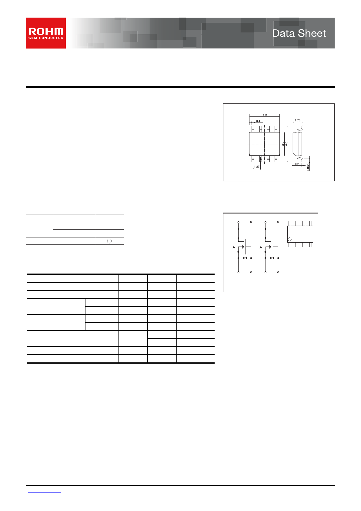
Structure Dimensions (Unit : mm)
Silicon N-channel MOSFET
Features
1) Built-in G-S Protection Diode.
2) Small surface Mount Package (SOP8).
Application
Power switching, DC / DC converter, Inverter
Packaging specifications Inner circuit
Type
SH8K22
Package
Code
Basic ordering unit (pieces)
Taping
TB
2500
Absolute maximum ratings (Ta=25C)
<It is the same ratings for the Tr1 and Tr2.>
Drain-source voltage
Gate-source voltage
Drain current
Source current
(Body diode)
Total power dissipation
Chanel temperature
Range of Storage temperature
*1 PW 10
*2 Mounted on a ceramic board
Parameter
s、
Duty cycle 1
Continuous
Pulsed
Continuous
Pulsed
Symbol Limits Unit
V
DSS
V
GSS
I
D
I
DP *1
I
S
I
SP *1
P
D *2
T
ch
T
stg
45 V
±20 V
±4.5 A
±18 A
1A
18 A
2 W / TOTAL
1.4 W / ELEMENT
150
-55 to +150
o
C
o
C
SOP8
Each lead has same dimensions
(8) (7)
∗2
∗1
(1) (2)
∗1 ESD PROTECTION DIODE
∗2 BODY DIODE
∗A protection diode is included between the gate and
the source terminals to protect the diode against static
electricity when the product is in use. Use the protection
circuit when the fixed voltages are exceeded.
(6) (5)
∗2
∗1
(3) (4)
(8) (7) (6) (5)
(1) (2) (3) (4)
(1) Tr1 Source
(2) Tr1 Gate
(3) Tr2 Source
(4) Tr2 Gate
(5) Tr2 Drain
(6) Tr2 Drain
(7) Tr1 Drain
(8) Tr1 Drain
www.rohm.com
1/4
c
○
2009 ROHM Co., Ltd. All rights reserved.
2009.12 - Rev.A

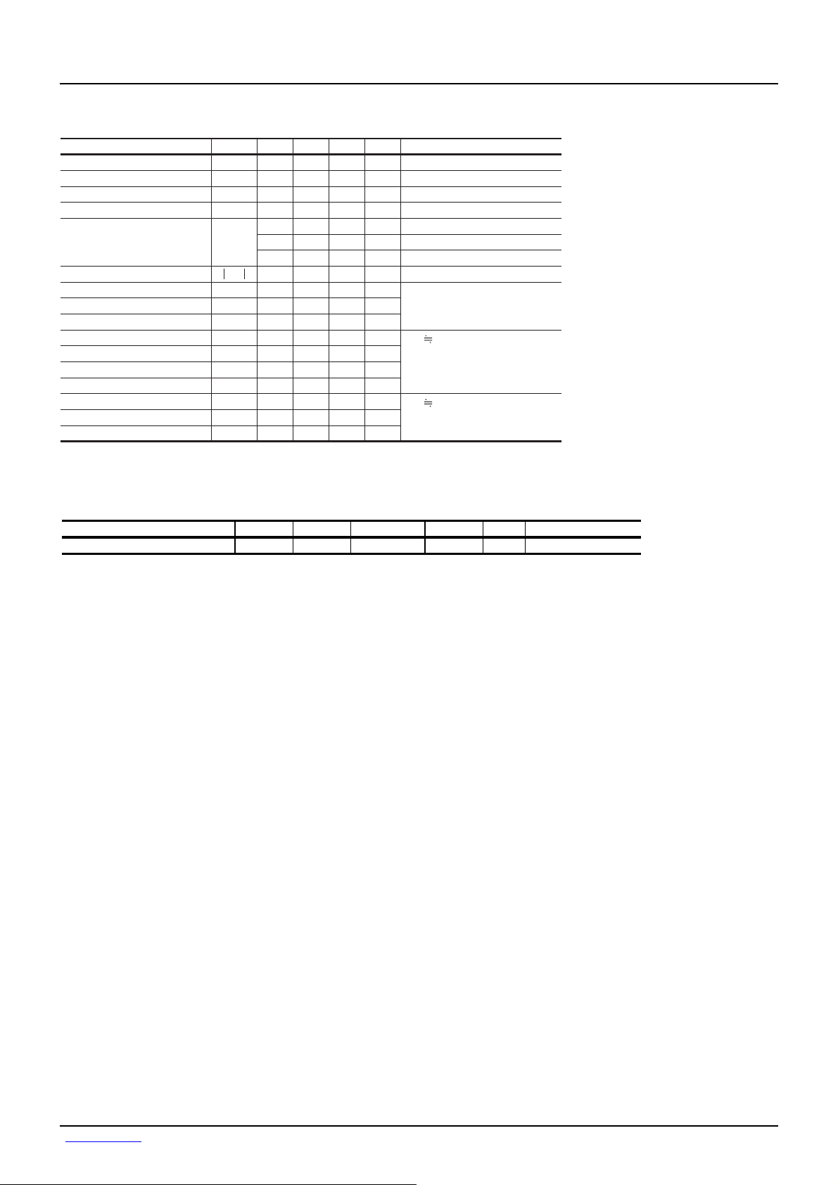
Electrical characteristics (Ta=25C)
<It is the same characteristics for the Tr1 and Tr2.>
Parameter Symbol
Gate-source leakage
Drain-source breakdown voltage
V
(BR) DSS
Zero gate voltage drain current
Gate threshold voltage
Static drain-source on-state
resistance
V
R
Forward transfer admittance
Input capacitance
Output capacitance
Reverse transfer capacitance
Turn-on delay time
Rise time
Turn-off delay time
Fall time
Total gate charge
Gate-source charge
Gate-drain charge
∗Pulsed
Body diode characteristics (Source-Drain) (Ta=25C)
<It is the same characteristics for the Tr1 and Tr2.>
Forward voltage
* pulsed
Parameter Condition
Min.−Typ. Max.
I
GSS
−±10 μAVGS=±20V, VDS=0V
45 −−VID= 1mA, VGS=0V
I
DSS
GS (th)
−−1 μAV
1.0 − 2.5 V V
− 33 46 I
∗
DS (on)
− 41 57 mΩ
− 46 64 I
∗
3.5 −−SV
Y
fs
C
C
C
t
d (on)
t
d (off)
Q
Q
Q
− 550 − pF V
iss
− 14070− pF V
oss
−
rss
∗
∗
t
r
∗
∗
t
f
∗
g
∗
gs
∗
gd
12
−
18
−
42
−
12
−
6.8
−
2.0
−
2.9
−−nC R
− pF f=1MHz
− ns
− ns
− ns
− ns
9.6 nC
− nC I
Symbol Min. Typ. Max. Unit
*
V
SD
--
Unit
mΩ
mΩ
D
I
D
D
V
ID= 2.5A
V
R
R
V
D
Conditions
= 45V, VGS=0V
DS
= 10V, ID= 1mA
DS
= 4.5A, VGS= 10V
= 4.5A, VGS= 4.5V
= 4.5A, VGS= 4.0V
= 10V, ID= 4.5A
DS
= 10V
DS
=0V
GS
DD
25V
GS
= 10V
L
= 10Ω
G
=10Ω
25V, VGS= 5V
DD
= 4.5A
= 5.6Ω, RG= 10Ω
L
1.2 V
I
=4.5A/VGS=0V
S
Data Sheet SH8K22
www.rohm.com
2/4
c
○
2009 ROHM Co., Ltd. All rights reserved.
2009.12 - Rev.A
 Loading...