

Page 1

Sensors Sensors
Sensors
Emitters
(1) Infrared LEDs
(1) Principle
In the absence of an externally applied voltage, the P-N
junction of a diode will be at thermal equilibrium and the
Fermi levels of the P layer and N layer will be equal (Fig.
1 (a)). In this case, the height of the potential barrier will
D.
be V
940 to 950 nm, and the response time is approximately
1µs.
GaAlAs infrared chips designed for higher output are
shown in Figure 3. The emitted wavelength of the chip of
Figure 3 (a) is 940 to 950 nm and the output is approximately 1.3 to 1.5 times that of the GaAs chip of Figure 2.
The chip of Figure 3 (b) is a so-called N-side up chip with
an emission wavelength of 880 nm. It produces a high
output, approximately 1.5 times that of the GaAs chip of
Figure 2. The response times of both chips of Figure 3
are approximately 1µs, the same as the chip of Figure 2.
When an external voltage V
rier falls to V
D - VF and electrons flow into the P layer and
F is applied, the potential bar-
holes into the N layer.
As carriers (holes and electrons) flow, they recombine,
and at that time the difference in energy before and after
recombination is released as light. The wavelength of the
emitted light is given by the following equation :
∆E = hν
Eg
ν = c / λ thus
hc
λ =
Eg
where λ is the wavelength of the emitted light, E
1.24
Eg
103 (nm)
g is the
energy band gap (1.35 ev in the case of GaAs), ∆E is the
energy difference before and after recombination, h is
Planck’s constant, ν is the frequency of the emitted light,
and c is the speed of light. The result is a peak emission
wavelength for GaAs of 940 to 950 nm.
The structure of a GaAs infrared chip is shown in Figure
2. The P-N junction of the GaAs-doped silicon is formed
by LPE (liquid crystal growth method). The luminous efficiency of the chip is 8 to 16%, the emitted wavelength is
(2) Structures
The structures of infrared LEDs can be divided into the
two following types.
161
Page 2
Sensors Sensors
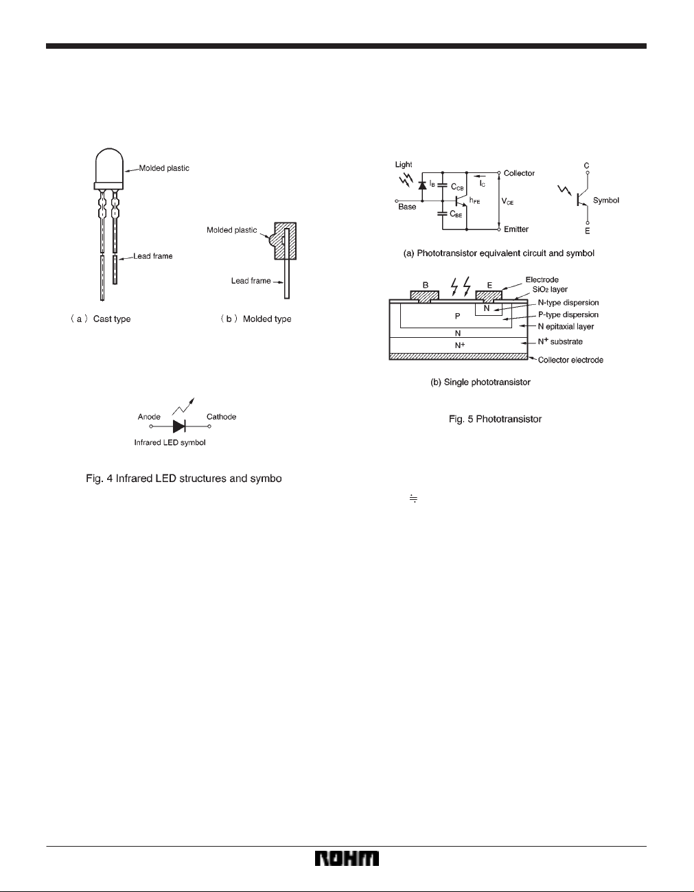
1. Cast type
The chip is mounted on a lead frame and then liquid resin
is poured into the mold and allowed to harden.
2. Molded type
This type is packaged by transfer molding.
Detectors
(1) Phototransistors
(1) Principle
As shown by the equivalent circuit in Figure 5 (a), a phototransistor can be thought of as a photodiode connected
to a normal silicon planar transistor.
Actual phototransistor structures are as shown in (b) of
Figure 5, and consist of a single type. The principle of operation is essentially amplification by an NPN transistor
of photo current generated by light irradiation.
C hFEIB
I
IB : Photo current of photodiode
FE : Transistor amplification of direct current
h
Like photodiodes, phototransistors are sensitive to a
wavelength of approximately 1100 nm.
(2) Structure
Like photodiodes, phototransistors are housed in the following three types of packages :
1. Cast type
2. Mold type
These are explained in detail on the infrared LED page.
162
Page 3

Sensors Sensors
(2) Photo ICs
(1) Principle
A photo IC is an integration of a photodiode, constant
voltage circuit, Schmitt trigger and other elements into a
single chip using bipolar IC technology . The structure of
a photodiode is shown in Figure 6 and a block diagram
is shown in Figure 7.
Multi-element devices
(1) Photointerrupters
Photointerrupters are also called transparent photosen-
sors, and they consist of an emitter and a detector facing
each other. Detection occurs when an object interrupts
the light beam passing from the emitter to the detector.
ROHM calls this transparent type of photosensor an interrupter.
The emitter is a high-output GaAs infrared LED with long
life, and the detector is normally a single phototransistor
or a photo IC.
Interrupters are generally housed in case-insertion packages or double-layer molding packages (Figure 8).
Case-insertion types are most commonly used, and consist of an emitter and detector inserted in an injection
molded case. The double-layer molding package responds to recent needs for increasingly compact devices.
This photo IC is a detector with digital output. When irradiated by light, one type has high transistor output and
another type has low output. Both types can be directly
connected to TTL, CMOS and other logic circuits with the
advantages of easy circuit design, space conservation,
and low cost.
(2) Structure
The external dimensions of a photo IC are shown in Figure 12. As there are normally three leads, V
GND, molded packages are the most common.
CC, VO and
The double-layer molding is carried out by injection
which makes it easy to achieve a compact package. This
device is ideal for cameras, floppy disk drives, handy
copy machines, and other applications where compactness is required.
(2) Photoreflectors
Photoreflectors are reflective-type photosensors consisting of an emitter and a detector facing the same direction. As light reflected from an object is detected, the output level is generally low. Thus a single silicon
phototransistor is used for the detector. The principal
structures are shown in Figure 9.
163
Page 4

Sensors Sensors
(3) Photo IC interrupters
Photo IC interrupters essentially take the output of a phototransistor (single or Darlington) and convert it to photo
IC output. The output is digital, with one type high and
another type low when irradiated with light.
In addition, there is a type with a connector attached for
easy handling as shown in (b) of Figure 10, and these are
used in facsimile machines and copiers.
164
Page 5

Appendix
No technical content pages of this document may be reproduced in any form or transmitted by any
means without prior permission of ROHM CO.,LTD.
The contents described herein are subject to change without notice. The specifications for the
product described in this document are for reference only. Upon actual use, therefore, please request
that specifications to be separately delivered.
Application circuit diagrams and circuit constants contained herein are shown as examples of standard
use and operation. Please pay careful attention to the peripheral conditions when designing circuits
and deciding upon circuit constants in the set.
Any data, including, but not limited to application circuit diagrams information, described herein
are intended only as illustrations of such devices and not as the specifications for such devices. ROHM
CO.,LTD. disclaims any warranty that any use of such devices shall be free from infringement of any
third party's intellectual property rights or other proprietary rights, and further, assumes no liability of
whatsoever nature in the event of any such infringement, or arising from or connected with or related
to the use of such devices.
Upon the sale of any such devices, other than for buyer's right to use such devices itself, resell or
otherwise dispose of the same, no express or implied right or license to practice or commercially
exploit any intellectual property rights or other proprietary rights owned or controlled by
ROHM CO., LTD. is granted to any such buyer.
Products listed in this document use silicon as a basic material.
Products listed in this document are no antiradiation design.
Notes
The products listed in this document are designed to be used with ordinary electronic equipment or devices
(such as audio visual equipment, office-automation equipment, communications devices, electrical
appliances and electronic toys).
Should you intend to use these products with equipment or devices which require an extremely high level of
reliability and the malfunction of with would directly endanger human life (such as medical instruments,
transportation equipment, aerospace machinery, nuclear-reactor controllers, fuel controllers and other
safety devices), please be sure to consult with our sales representative in advance.
About Export Control Order in Japan
Products described herein are the objects of controlled goods in Annex 1 (Item 16) of Export Trade Control
Order in Japan.
In case of export from Japan, please confirm if it applies to "objective" criteria or an "informed" (by MITI clause)
on the basis of "catch all controls for Non-Proliferation of Weapons of Mass Destruction.
Appendix1-Rev1.0
 Loading...