How it Works
Log In / Sign Up
Buy Points
How it Works
FAQ
Contact Us
Questions and Suggestions
Users
ROHM
Loading...
R
RSD150N06
RSD175N10
RSD200N05
RSE002N06
RSE002P03
RSF010P05
RSF014N03
RSH065N06
RSH070N05
RSH070P05
RSJ250P10
RSJ300N10
RSJ450N04
RSJ550N10
RSJ650N10
RSM002N06
RSM002P03
RSQ015N06
RSQ015P10
RSQ020N03
RSR010N10
RSR015P03
RSR020N06
RSR020P03
RSR025N03
RSR030N06
RSU002N06
RSU002P03
RT1A045AP
RT1A050ZP
RT1A060AP
RT1C060UN
RT1E040RP
RT1E050RP
RT1E060XN
RTF015N03
RTF016N05
RTF025N03
RTL035N03
RTQ020N03
RTQ020N05
RTQ025P02
RTQ030P02
RTQ035N03
RTQ045N03
RTR020N05
RTR025N03
RTR025N05
RTR040N03
RU1C002UN
RU1C002ZP
RU1E002SP
RU1L002SN
RUC002N05
RUE002N02
RUE002N05
RUF015N02
RUF020N02
RUF025N02
RUL035N02
RUM002N05
RUQ050N02
RUR040N02
RUU002N05
RVQ040N05
RW1A013ZP
RW1A020ZP
RW1A025AP
RW1A030AP
RW1C015UN
RW1C020UN
RW1C025ZP
RW1E015RP
RW1E025RP
RXH070N03
RXH090N03
RXH100N03
RXH125N03
RXQ040N03
RXR035N03
RYC002N05
RYE002N05
RYM002N05
RYU002N05
RZE002P02
RZF013P01
RZF020P01
RZF030P01
RZL025P01
RZM002P02
RZP
RZP-A
RZQ045P01
RZQ050P01
RZR020P01
RZR025P01
RZR040P01
S
SBGA024W040
SBGA063W060
SBGA099W070
Loading...
Loading...
Nothing found
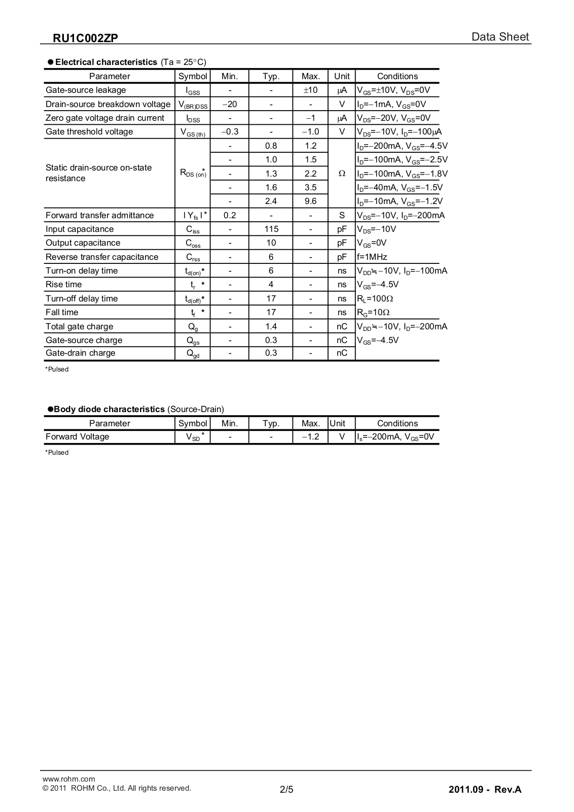
RU1C002ZP
Technical data
6 pgs
992.55 Kb
0
Table of contents
Loading...
ROHM RU1C002ZP Technical data
...
ROHM Technical data
Download
Specifications and Main Features
Frequently Asked Questions
User Manual
Download
Loading...
+
hidden pages
Unhide
You need points to download manuals.
1 point = 1 manual.
You can buy points or you can get point for every manual you upload.
Buy points
Upload your manuals
 Loading...