

Transistor
DC-DC Converter (−20V, −3.0A)
RTQ030P02
zFeatures
1) Low On-resistance.(110mΩ at 2.5V)
2) High Power Package.
3) High speed switching.
4) Low voltage drive.(2.5V)
zApplications
DC-DC converter
zStructure
Silicon P-channel
MOSFET
zPackaging specifications
Package
Type
RTQ030P02
Code
Basic ordering unit
(pieces)
Taping
TR
3000
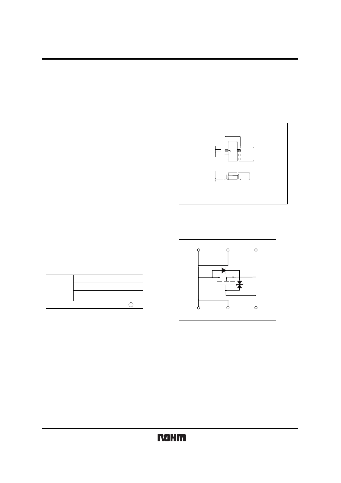
zExternal dimensions (Units : mm)
TSMT6
2.8
1.6
)
1
(
)
2
(
0.4
)
3
(
0.16
Abbreviatedsymbol : TS
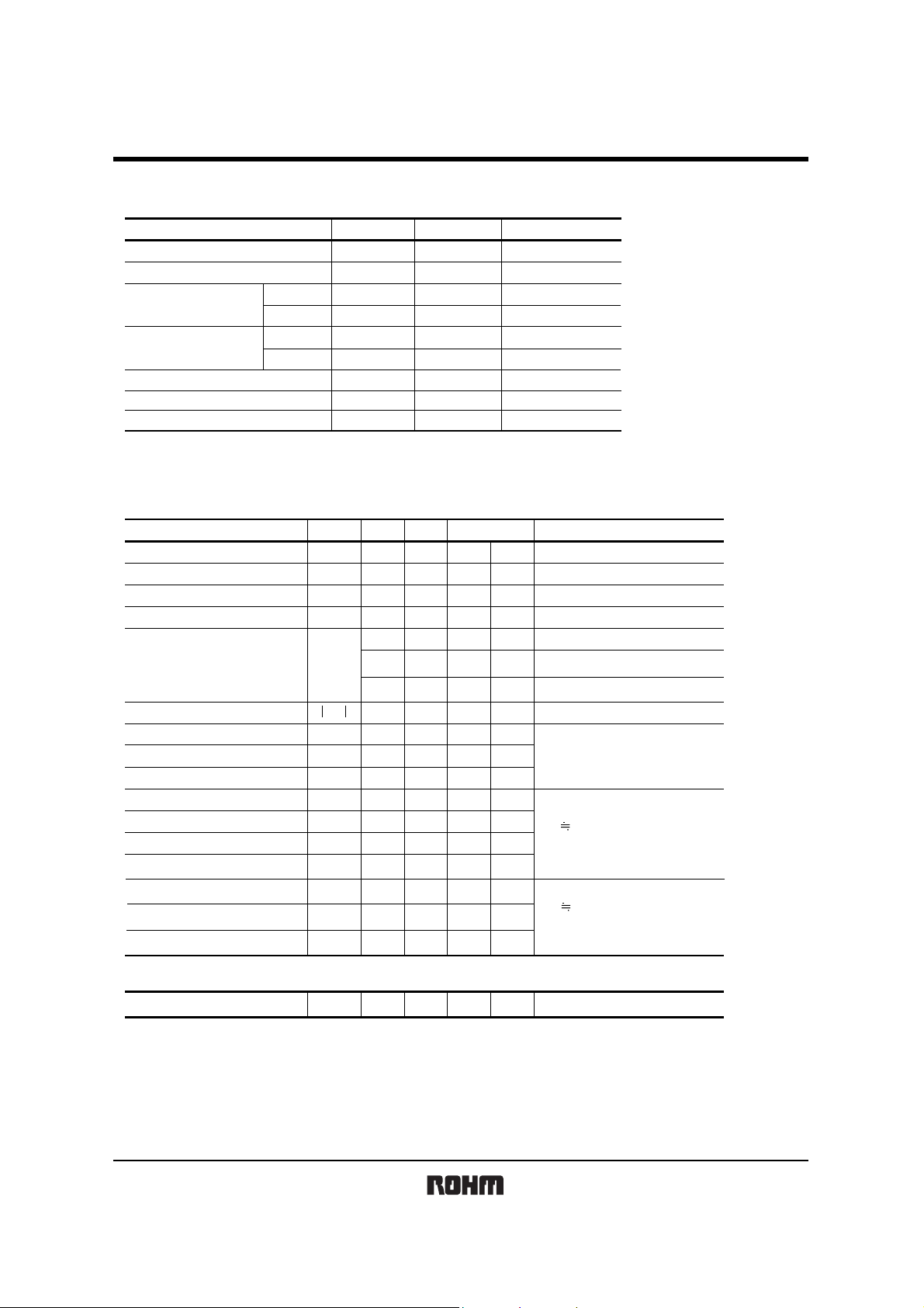
zEquivalent circuit
∗2
(1)
∗1 ESD PROTECTION DIODE
∗2 BODY DIODE
(2) (3)
RTQ030P02
(6)(5)(4)
2.9
0.85
Each lead has same dimensions
(4)(5)(6)
∗1
(1)DRAIN
(2)DRAIN
(3)GATE
(4)SOURCE
(5)DRAIN
(6)DRAIN
1/4
Transistor
zAbsolute maximum ratings (Ta=25°C)
I
V
(BR)DSS
I
V
R
DS(on)
Y
C
C
C
d(on)
t
t
d(off)
Qg
Qgs
Qgd
VSD
GSS
DSS
GS(th)
fs
iss
oss
rss
r
t
t
f
Symbol
V
V
I
I
P
Tch
Tstg
∗
∗
∗
∗
∗
∗
DSS
GSS
I
D
DP
I
S
SP
D
Min.
−20
−0.7
2.0
−
−
−
−
−
−
−
−
−
−
−
−
−
−
−
−
Parameter
Drain−source voltage
Gate−source voltage
Drain current
Source current
(Body diode)
Continuous
Pulsed
Continuous
Pulsed
Total power dissipation
Channel temperature
Range of Storage temperature
<
∗1 Pw 10µs, Duty cycle 1%
=
∗2 Mounted on a ceramic board
<
=
zElectrical characteristics (Ta=25°C)
Parameter Symbol
Gate-source leakage
Drain-source breakdown voltage
Zero gate voltage drain current
Gate threshold voltage
Static drain-source on-state
resistance
Foward transfer admittance
Input capacitance
Output capacitance
Reverse transfer capacitance
Turn-on delay time
Rise time
Turn-off delay time
Fall time
Total gate charge
Gate-source charge
Gate-drain charge
∗PULSED
Body diode characteristics (source-drain characteristics)
Forward voltage
Limits Unit
−20
±12
±3
±12
−1
−4
1.25
150
−55~+150
Typ. Max.
−
−
−
−
60
Unit
±10
−
−1
−2.0
80
65 90
110
150
−
−
800
150
100
15
27
50
20
9.0
1.6
4.6
−
−
−
−
−
−
−
−
−
−
−1.2
−
µA
V
µA
V
mΩ
mΩ
mΩ
S
pF
pF
pF
ns
ns
ns
ns
nC
nC
nC
V
V
I
V
V
I
I
V
V
V
A
∗1
A
A
∗1
A
∗2
W
°C
°C
Conditions
GS
=±12V, VDS=0V
mA,
D
=−1 , VGS=0V
DS
=−20V, VGS=0V
DS
=−10V, ID=−1
D
=−3A, VGS=−4.5V
D
=−3A, VGS=−4V
D
=−1.5A, VGS=−2.5V
I
DS
=−10V, ID=−1.5A
V
GS
DS
=−10V,
V
=1MHz
f
D
=−1.5A
I
DD
V
V
GS
=−4.5V
L
=10Ω
R
R
GS
=10Ω
V
DD
GS
=−4.5V
V
I
D
=−3A
I
S
=−1A, VGS=0V
=0V
−15V
−15V
RTQ030P02
mA
2/4
 Loading...