

Data Sheet
4V Drive Nch MOSFET
RSD175N10
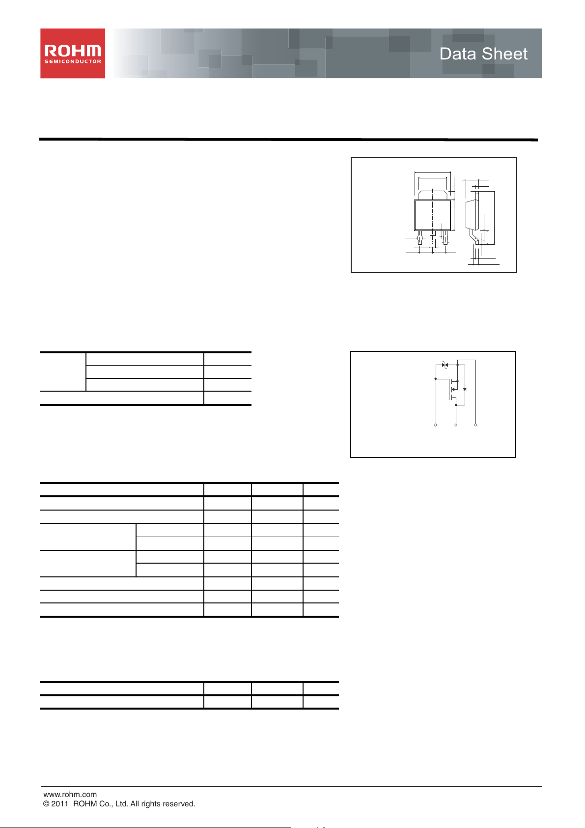
Structure Dimensions (Unit : mm)
Silicon N-channel MOSFET
Features
1) Low on-resistance.
4) 4V drive.
4) High power package.
Application
Switching
CPT3
(SC-63)
<SOT-428>
0.75
6.5
5.1
0.9
0.65
2.30.9
(1)
(3)
(2)
2.3
0.5
1.5
5.5
2.3
1.5
0.8Min.
0.5
1.0
9.5
2.5
Packaging specifications Inner circuit
Package Taping
Type
Code TL
Basic ordering unit (pieces) 2500
RSD175N10
(1) Gate
(2) Drain
(3) Source
Absolute maximum ratings (Ta = 25C)
Parameter
Drain-source voltage V
Gate-source voltage V
Drain current
Source current
(Body Diode)
Continuous I
Pulsed I
Continuous I
Pulsed I
Power dissipation P
Symbol Limits Unit
DSS
GSS
D
DP
S
SP
D
*3
*1
*3
*1
*2
100 V
20 V
17.5 A
35 A
17.5 A
35 A
20 W
Channel temperature Tch 150 C
Range of storage temperature Tstg 55 to 150 C
*1 PW10s, Duty cycle1%
=25°C
*2 T
C
*3 Please use within the range of SOA.
∗1
∗2
(1) (2) (3)
∗1 ESD PROTECTION DIODE
∗2 BODY DIODE
Thermal resistance
Parameter
Channel to Case Rth (ch-c) 6.25 C / W
* TC=25°C
www.rohm.com
© 2011 ROHM Co., Ltd. All rights reserved.
Symbol Limits Unit
*
1/6
2011.06 - Rev.A
www.rohm.com
© 2011 ROHM Co., Ltd. All rights reserved.
Data Sheet
RSD175N10
Electrical characteristics (Ta = 25C)
Parameter
Symbol Min. Typ. Max. Unit
Gate-source leakage I
Drain-source breakdown voltage V
Zero gate voltage drain current I
Gate threshold voltage V
GSS
(BR)DSS
DSS
GS (th)
--10 AVGS=20V, VDS=0V
100 - - V ID=1mA, VGS=0V
--1AVDS=100V, VGS=0V
1 - 2.5 V VDS=10V, ID=1mA
Conditions
- 75 105 ID=8.8A, VGS=10V
Static drain-source on-state
resistance
R
DS (on)
*
- 80 112 ID=8.8A, VGS=4.5V
m
- 85 119 ID=8.8A, VGS=4V
*
iss
oss
rss
d(on)
d(off)
gd
*
- 950 - pF VDS=25V
- 85 - pF VGS=0V
- 55 - pF f=1MHz
- 10 - ns VDD 50V, ID=8.8A
*
*
- 25 - ns VGS=10V
*
*
r
- 60 - ns RL=5.7
*
*
- 50 - ns RG=10
*
*
f
- 24 - nC VDD 50V, ID=17.5A
*
*
g
-3-nCV
*
*
gs
-6-nC
*
*
GS
=10V
Forward transfer admittance l Yfs l5 - - SVDS=10V, ID=8.8A
Input capacitance C
Output capacitance C
Reverse transfer capacitance C
Turn-on delay time t
Rise time t
Turn-off delay time t
Fall time t
Total gate charge Q
Gate-source charge Q
Gate-drain charge Q
*Pulsed
Body diode characteristics (Source-Drain)
Parameter
Forward Voltage V
*Pulsed
Symbol Min. Typ. Max. Unit
*
SD
Conditions
- - 1.5 V Is=17.5A, VGS=0V
2/6
2011.06 - Rev.A
www.rohm.com
© 2011 ROHM Co., Ltd. All rights reserved.
Data Sheet
RSD175N10
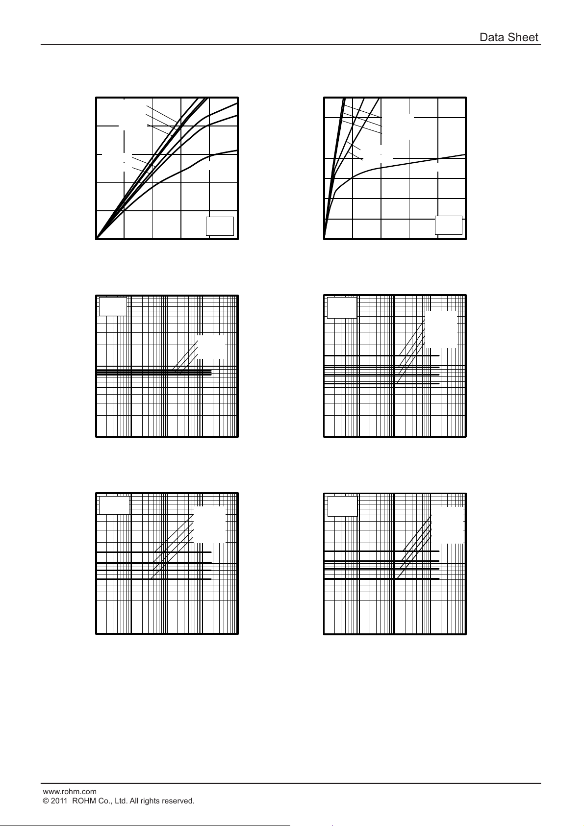
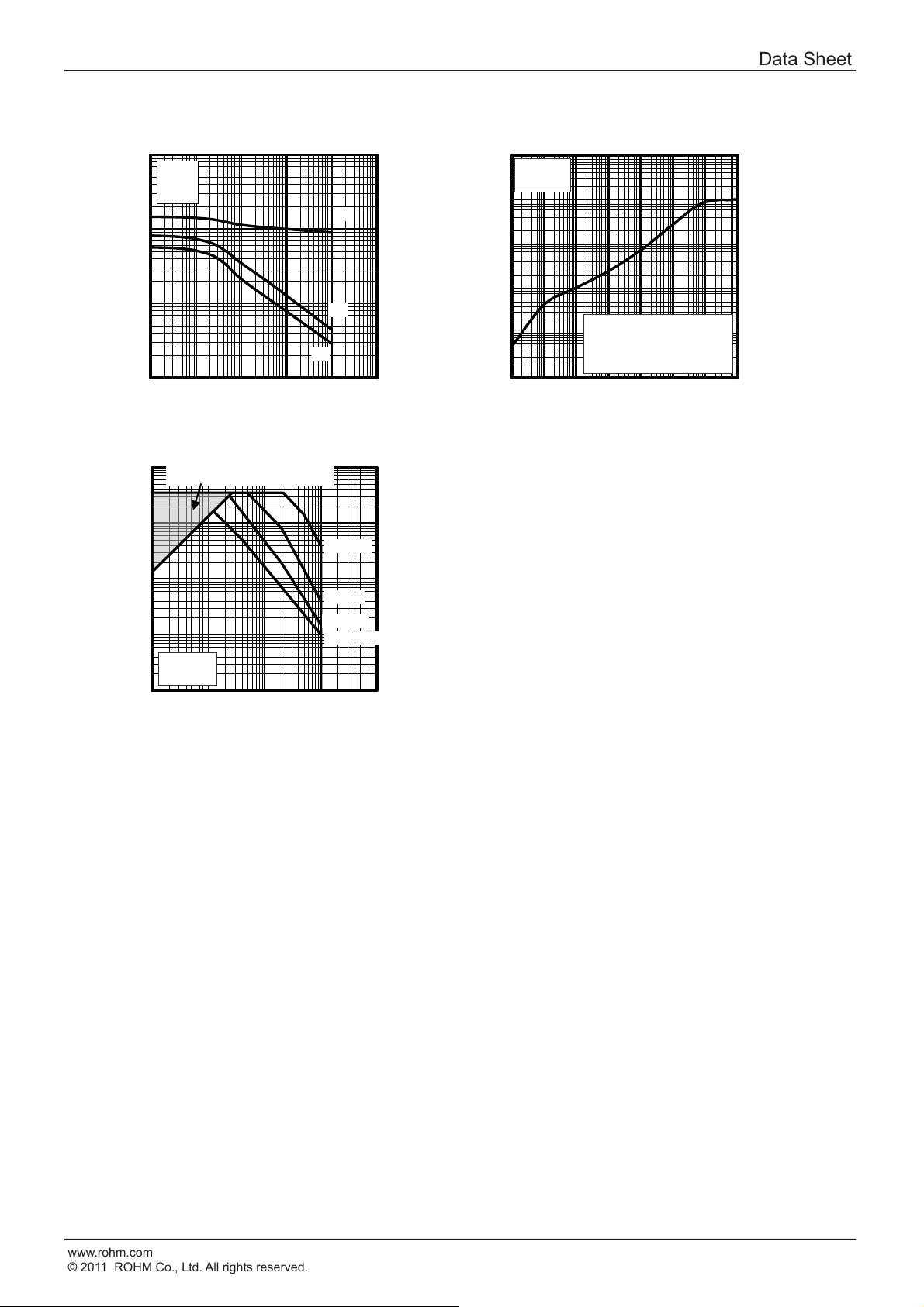
Electrical characteristic curves (Ta=25C)
0
2
4
6
8
10
0 0.2 0.4 0.6 0.8 1
Drain Current : I
D
[A]
Drain-Source Voltage : VDS [V]
Fig.1 Typical Output Characteristics (Ⅰ)
VGS=2.5V
Ta=25°C
pulsed
VGS=10.0V
VGS=4.0V
VGS=4.5V
VGS=2.8V
VGS=3.0V
0
2.5
5
7.5
10
12.5
15
17.5
0 2 4 6 8 10
Drain Current : I
D
[A]
Drain-Source Voltage : VDS [V]
Fig.2 Typical Output Characteristics (Ⅱ)
VGS=2.5V
VGS=10.0V
VGS=4.0V
VGS=4.5V
VGS=2.8V
VGS=3.0V
Ta=25°C
pulsed
10
100
1000
0.01 0.1 1 10 100
Static Drain-Source On-State Resistance
R
DS(on)
[mΩ]
Drain Current : ID [A]
Fig.3 Static Drain-Source On-State Resistance vs. Drain Current
VGS=4.0V
VGS=4.5V
VGS=10V
Ta=25°C
pulsed
10
100
1000
0.01 0.1 1 10 100
Static Drain-Source On-State Resistance
R
DS(on)
[mΩ]
Drain Current : ID [A]
Fig.4 Static Drain-Source On-State Resistance vs. Drain Current
VGS=10V
pulsed
T
a
=125°C
T
a
=75°C
T
a
=25°C
T
a
=-25°C
10
100
1000
0.01 0.1 1 10 100
Static Drain-Source On-State Resistance
R
DS(on)
[mΩ]
Drain Current : ID [A]
Fig.5 Static Drain-Source On-State Resistance vs. Drain Current
V
GS
=4.5V
pulsed
Ta=125°C
Ta=75°C
Ta=25°C
Ta=-25°C
10
100
1000
0.01 0.1 1 10 100
Static Drain-Source On-State Resistance
R
DS(on)
[mΩ]
Drain Current : ID [A]
Fig.6 Static Drain-Source On-State Resistance vs. Drain Current
V
GS
=4V
pulsed
Ta=125°C
Ta=75°C
Ta=25°C
Ta=-25°C
3/6
2011.06 - Rev.A
www.rohm.com
© 2011 ROHM Co., Ltd. All rights reserved.
Data Sheet
RSD175N10
0.01
0.1
1
10
100
0.01 0.1 1 10 100
Forward Transfer Admittance
Y
fs
[S]
Drain Current : ID [A]
Fig.7 Forward Transfer Admittance vs. Drain Current
VDS=10V
pulsed
Ta=125°C
Ta=75°C
Ta=25°C
Ta=-25°C
0.001
0.01
0.1
1
10
100
0.0 0.5 1.0 1.5 2.0 2.5 3.0 3.5
Drain Currnt : I
D
[A]
Gate-Source Voltage : VGS [V]
Fig.8 Typical Transfer Characteristics
VDS=10V
pulsed
Ta=125°C
Ta=75°C
Ta=25°C
Ta=-25°C
0.01
0.1
1
10
100
0.0 0.5 1.0 1.5 2.0
Source Current : Is [A]
Source-Drain Voltage : VSD [V]
Fig.9 Source Current vs. Source-Drain Voltage
VGS=0V
pulsed
Ta=125°C
Ta=75°C
Ta=25°C
Ta=-25°C
0
50
100
150
200
250
0 2 4 6 8 10
Static Drain-Source On-State Resistance
R
DS(on)
[mΩ]
Gate-Source Voltage : VGS [V]
Fig.10 Static Drain-Source On-State Resistance vs. Gate-Source
Voltage
ID=8.8A
ID=17.5A
Ta=25°C
pulsed
1
10
100
1000
10000
0.01 0.1 1 10 100
Switching Time : t [ns]
Drain Current : ID [A]
Fig.11 Switching Characteristics
t
d(on)
t
r
t
t
VDD≒50V
VGS=10V
RG=10Ω
Ta=25°C
Pulsed
0
2
4
6
8
10
0 5 10 15 20 25
Gate-Source Voltage : V
GS
[V]
Total Gate Charge : Qg [nC]
Fig.12 Dynamic Input Characteristics
T
a
=25°C
VDD=50V
I
D
=17.5A
Pulsed
4/6
2011.06 - Rev.A
www.rohm.com
© 2011 ROHM Co., Ltd. All rights reserved.
Data Sheet
RSD175N10
10
100
1000
10000
0.01 0.1 1 10 100 1000
Capacitance : C [pF]
Drain-Source Voltage : VDS [V]
Fig.13 Typical Capacitance vs. Drain-Source Voltage
Ta=25°C
f=1MHz
VGS=0V
C
iss
C
oss
C
rss
0.0001
0.001
0.01
0.1
1
10
0.0001 0.001 0.01 0.1 1 10 100 1000
Normalized Transient Thermal Resistance : r(t)
Pulse width : Pw (s)
Fig.14 Normalized Transient Thermal Resistance v.s. Pulse Width
T
a
=25°C
Single Pulse
Mounted on a recommended land.
(20mm
× 20mm × 0.8mm)
Rth
(ch-a)
=103.5°C/W
Rth
(ch-a)
(t)=r(t)×Rth
(ch-a)
0.01
0.1
1
10
100
0.1 1 10 100 1000
Drain Current : I
D
[ A ]
Drain-Source Voltage : VDS [ V ]
Fig.15 Maximum Safe Operating Area
T
c
=25°C
Single Pulse
Operation in this area is limited
by R
DS(on)
(VGS = 10V)
PW = 100μs
PW = 1ms
PW = 10ms
DC Operation
5/6
2011.06 - Rev.A
www.rohm.com
© 2011 ROHM Co., Ltd. All rights reserved.
Data Sheet
RSD175N10
S
%
V
V
V
S
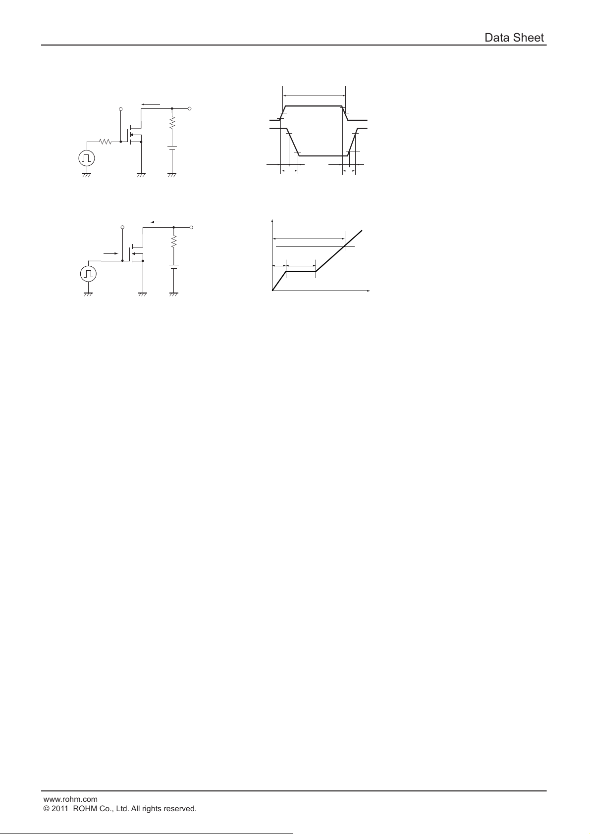
Measurement circuits
V
GS
R
G
D.U.T.
Pulse width
D
I
V
D
R
L
V
DD
50%
10%
GS
DS
10% 10%
t
d(on)
t
on
90%
50%
90% 90
t
d(off)
t
r
t
off
t
f
Fig.1-1 Switching Time Measurement Circuit
VGS
IG(Const.)
D.U.T.
D
I
VD
RL
VDD
Fig.2-1 Gate Charge Measurement Circuit
Fig.1-2 Switching Waveforms
V
G
Q
g
GS
QgsQ
gd
Charge
Fig.2-2 Gate Charge Waveform
6/6
2011.06 - Rev.A
Notes
Notice
www.rohm.com
© 2011 ROHM Co., Ltd. All rights reserved.
Thank you for your accessing to ROHM product informations.
More detail product informations and catalogs are available, please contact us.
ROHM Customer Support System
http://www.rohm.com/contact/
R1120A
 Loading...