

RPM972-H14
Photo Link Module
IrDA Infrared Communication Module
RPM972-H14
RPM972-H14 is an infrared communication module for IrDA Ver . 1.4 (Low Power). The infrared LED, PIN photo diode,
and waveform shaping LSI are all integrated into one single package. This module is designed for low power
consumption. The very small package makes it a perfect fit for mobile devices.
Also it provides the capability of IR remote control transmission for universal remote control applications.
zFeatures
1) Infrared LED, PIN photo diode, LED driver and receiver frequency formation circuit built in.
Improvement of EMI noise protection by Shield Case.
2) Applied to SIR (9.6k to 115.2kbps), MIR (0.576M, 1.152Mbps) and FIR(4Mbps).
3) Surface mount type.
4) Power down function bui lt in.
5) Adjustable communication distance by LED load resistance value.
6) Infrared remote control transmission driver built-in.
zApplications
Cellular phone, PDA, DVC, Digital still camera, Printer, Handy terminal etc.
zAbsolute maximum ratings (Ta=25°C)
Parameter Symbol Limits Unit
Supply voltage Vcc
Input voltage
Operation temperature
Storage temperature
∗1) This applies to all pins basis ground pin (8pin).
/
V
LEDA
/
Vin(3,4,5pin)
Topr
Tstg
V
zRecommended operating conditions
Parameter Symbol Min. Typ. Max. Unit
CC
V
Supply voltage
V
LEDA
V
IO
IO
−0.3 to V
∗1
6.5
IO
+0.3
−25 to 85
−30 to 100
3.0 V2.4 3.6
3.0 V2.7 5.5
3.0 V1.7 V
V
V
°C
°C
CC
1/9
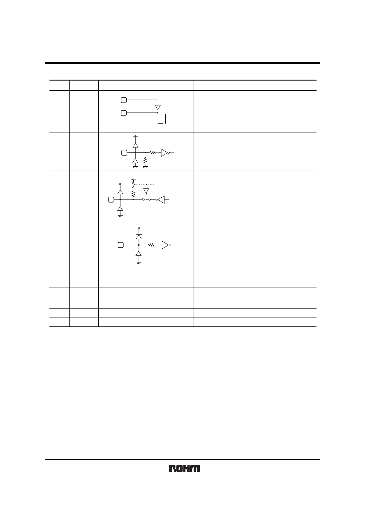
Photo Link Module
zT ermina l description
Terminal Circuit FunctionPin No
1 LEDA
RPM972-H14
1
LED
2
LED Anode Terminal
LED drive power supply.
Other power source can be used difference between
CC
and VCC.
LEDV
2 LEDC
3
TXD
RXD
4
PWDOWN
5
/Mode
V
CC
6
V
IO
7
8 GND
Shield Case
−
LED Cathode Terminal
IO
V
Transmitting Data Input Terminal
H:LED radiant (PWDOWN='L')
CMOS Logic Level Input.
Holding TXD="H"status, LED will be turn off
600k
V
300k
IO
V
PWDOWN
IO
V
IO
approximately 48 µs.
Receiving Data Output Terminal
When PWDOWN(5pin)='H', the RXD output will be pulled
up to V
IO
at approximately 300 kΩ.
Power-down Control and Mode SettingTerminal
H: POWERDOWN
L : OPERATION
CMOS Logic Level Input.
When input is "H", it will stop the receiving circuit, Pin−PD
current and transmitting LED operation.
V
CC
Supply voltage for Transceiver circuits.
V
IO
Supply voltage for I / O pins
(PWDOWN,RXD,TXD).
GROUND
Connect to Ground.
2/9
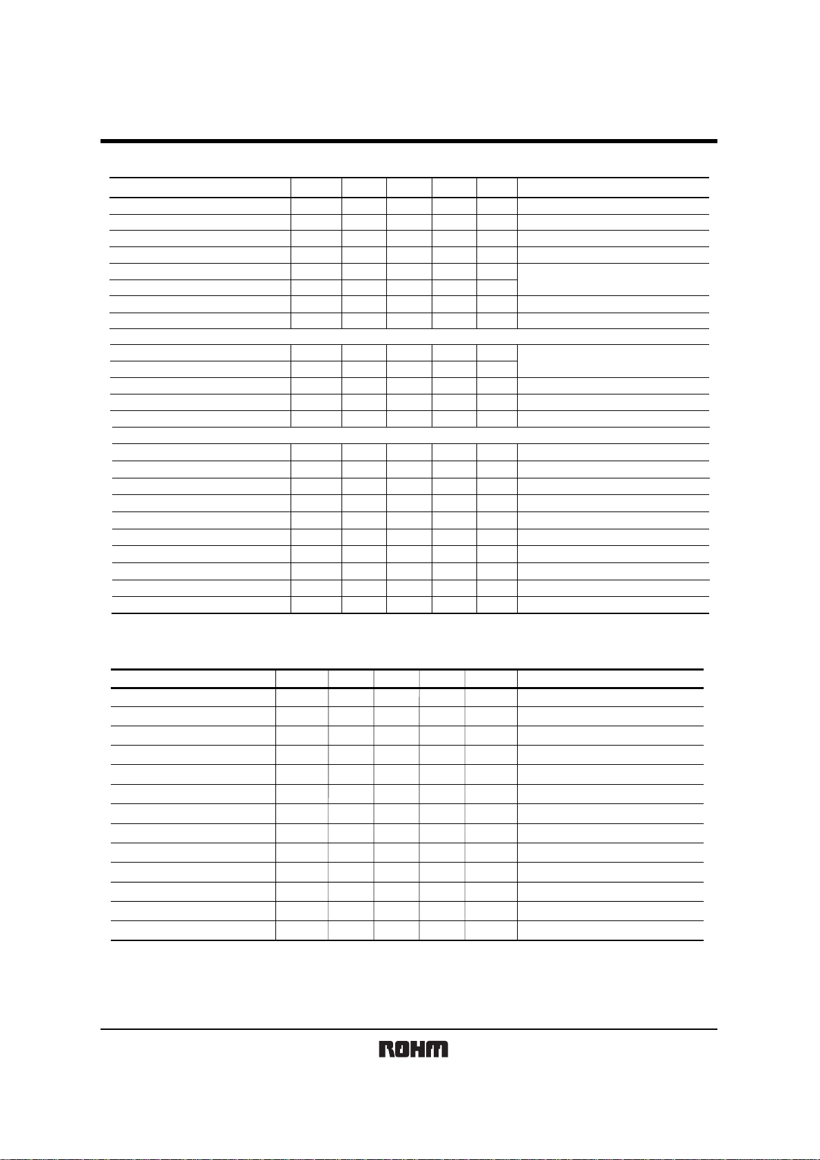
Photo Link Module
zElectrical characteristics (Unless otherwise noted, V
Parameter Symbol Min. Typ. Max. Unit Conditions
Consumption current 1(SIR / MIR mode)
Consumption current 2(FIR mode)
Consumption current 3(at PWDOWN) 0.01
ICC1
I
CC2
I
CC3
Transmission rate
PWDOWN input high voltage
PWDOWN input low voltage
PWDOWN input high current
PWDOWN input low current
VPDH
VPDL
IPDH
IPDL
< Transmitter >
TXD input high voltage
TXD input low voltage
TXD input high current
TXD input low current
LED anode current
VTXH
VTXL
ITXH
ITXL
ILED1
< Receiver >
RXD output high voltage
RXD output low voltage
RXD output rise time
RXD output fall time
RXD output pulse width(SIR)
VRXH
VRXL
tRR
tFR
twRXDS
RXD output pulse width(MIR1) twRXDM1 200 434 ns800
RXD output pulse width(MIR2) twRXDM2 100 217 ns500
twRXDF1
RXD output pulse width(FIR2)
Receiver latency time
twRXDF2
tRT
zOptical characteristics (Unless otherwise noted, V
Parameter Symbol Min. Typ. Max. Unit Conditions
Peak wave length
Intensity
Half−angle
Rise time / Fall time
λP
IE
θL / 2
Tr / Tf
880
Optical over shoot
Edge jitter
Optical pulse width(MIR)
Optical pulse width(FIR)
Minimum irradiance in angular 1
Minimum irradiance in angular 2
Maximum irradiance in angular
Input half−angle
Maximum emitting time
1. This product is not designed for protection against radioactive rays.
2. This product dose not include laser transmitter.
3. This product includes one PIN photo diode.
4. This product dose not include optical load.
Tj
TweM 172 217 256
TweF 115 125 135
Eemin1
Eemin2
Eemax
θD / 2
TLEDmax
−25
500
±15
CC=3V , VL EDV
400
400
800
1000
−µA
0.0096
2/3∗V
0
−1.0
−1.0
2/3∗V
0
2.5
−1.0
180
V
IO
−0.4
0
−
−
1.0
−
−
IO
−
1/3∗V
0
0
−
IO
−
1/3∗V
5
0
250
−
−
20
20
2.3
125RXD output pulse width(FIR1)
195 250 290
100
−
CC=3V , VLEDV
890 nm
10025
−
−
−
−
900
−
−
−
−
−
−
−
−
−±15
40
25
25
8
20
−
−−
16
48
120
=3V , VIO=3V, Ta=25°C)
CC
1600
1600
0.2
µA PWDOWN=0V, At no input light
µA
PWDOWN=0V, At no input light
PWDOWN=V
Mbps4
V
1.0
1.0
V
10
1.0
300
V
0.4
−
−
4.0
16585
200
CC
V
IO
IO
IO
IO
V
µA
µA
V
V
µA
µA
VIO=1.7 to 3.6 V
(V
PWDOWN=V
PWDOWN=0V
VIO=1.7 to 3.6 V
(VIO VCC)
TXD=V
TXD=0V
mA
V
IO
IRXH= −200µA
V
IRXL=200µA
ns
C
L=15pF
ns
C
L=15pF
µs
C
L=15pF, 9.6k to 115.2 kbps, duty19%
C
L=15pF, 0.576 Mbps, duty25%
L=15pF, 1.152 Mbps, duty25%
C
ns
L=15pF, 4 Mbps(125ns pulse)
C
ns
C
L=15pF, 4 Mbps(250ns pulse)
µs
=3V , VIO=3V, Ta=25°C)
−15 deg θ L 15 deg
/
sr
mW
deg
ns
10% to 90%
%
ns
ns
tTXD=217ns
ns
tTXD=125ns
2
µW / cm
µW
mW
−15 deg θ L 15 deg, 115.2kbps
2
−15 deg θ L 15 deg, 115.2kbps
/
cm
2
−15 deg θ L 15 deg
/
cm
deg
TXD=V
µs
RPM972-H14
IO
, At no input light
<
IO
VCC)
−
IO
<
−
IO
<−<
−
<−<
<−<
<−<
IO
−
−
−
<
−
<
3/9

RPM972-H14
Photo Link Module
zTiming chart
1. Mode Setting (SIR / MIR / FIR)
With RPM972-H14 there is a need for mode s witch accor ding to c ommun icati on rate. F or th e mode s etting, ther e
are “PWDOWN/Mode” and “TXD”. Please see below diagram for the set up of mode.
(a) FIR Mode
(b) SIR / MIR Mode
PWDOWN
/
Mode
TXD
Mode
>
ts 200ns
=
>
ts 200ns
=
tdmax=200µs
FIR Mode
(4Mbps)
PWDOWN
/
Mode
TXD
Mode
tdmax=200µs
Fig. 1
2. Remote control transmitting
When remote control signal is input to the TXD terminal, remote control is transmitted.
3. Timing chart (use example)
(a) Emitting
When a pulse is inputted to TXD terminal, LED is emitting, and a signal is transmitted.
But, when “H” condition follows TXD terminal , LED turns of f the lights in the range of TLEDmax.
SIR / MIR Mode
(9.6k-1.152Mbps)
TXD
more than TLEDmaxless than TLEDmax
(IrDA/RC emitting)(IrDA/RC emitting)(IrDA/RC emitting)
LED emitting
TLEDmax
PWDOWN
4/9

RPM972-H14
Photo Link Module
(b) Detecting
When it is received an optical si gnal, a signal outpu ts from RXD termina l at the following timi ng.
It is outputted in the pulse width fixed at the time of SIR mode (9.6k to 115.2kbps).
It is outputted in the pulse width which is the same as the input signal at the time of MIR mode (0.576M, 1.152Mbps)
and FIR mode (4Mbps).
But, as for the pulse width of the input signal, it is based on IrDA Physical Layer Specification.
1 SIR mode (output example)
Light input
RXD
PWDOWN
2 MIR mode (output example)
Light input
RXD
PWDOWN
3 FIR mode (output example)
less than 2.3µs
∗ more than 1.41µS
approximately 2.3µs
434ns 217ns
434ns 217ns
more than 2.3µs
300kΩ pull up
300kΩ pull up
Light input
RXD
PWDOWN
125ns 250ns
300kΩ pull up
125ns 250ns
5/9

Photo Link Module
zDimensions (Unit : mm)
RPM972-H14
R1.0
2.2
1.0
2.67
LED
0.6±0.1
1.1
1.4
2.8
4.0
A
P0.95×7=6.65
0.6
8.0
PinPD
0.37±0.1
0.95
0.48
R1.1
2.2
0.15±0.1
0.78
2.59
0.15±0.1
2.9
81
(0.13)
0.68±0.1
A Part Size (Shield Case underside size)
NOTE
1. TOLERANCE : ±0.2mm
2. COPLANARITY : 0.1mmMAX
UNIT : mm
ETH871
0.76
2.2
0.75
6/9

Photo Link Module
zBlock diagram and application circuit
RPM972-H14
AMP
AMP
AMP
POWER
DOWN
/Mode
LEDA
18765432
LEDC
TXD
RXD
PWDOWN/Mode
V
CC
C1
V
IO
GND
Transmitter
signal
Receiver
signal
LEDV
IrDA/RC
Controller
V
CC
V
IO
GND
CC
zAttac hed components
Part symbol Recommended value
C1
6.8µF, Ceramic or tantalum
Ex.)TCFGA1A685M8R(ROHM)
Notice
Bigger capacitance is recommended with
much noise from power supply.
7/9

RPM972-H14
Photo Link Module
zNotes
1) VLEDV
•
There is no problem even if it is supplied separately from each power supply such as a fix voltage power supply and a
battery power supply. (V
But, use it in the recommendation power supply voltage range.
2) Caution in designing bo ard lay-out
T o get maximum potential from RPM972-H14, please keep in mind following instruction.
•
The line of RXD (4pin) should be connected at backside via through hole close to RPM972-H14 pin lead. Better not
to be close to photo diode side (8pin side).
⇒This is to mini mize feedback supplied to photo diode from RXD.
•
The parts which generate noise such as DC / DC converter should be one’s placed at more than a radius of 1.0cm
away from photo diode (8pin side).
•
As for C1 between 6 - 8 pins, it should be one’s placed close to RPM972-H14.
3) Notes
•
Please be sure to set up the TXD (3pin) input to be “L” (under 0.6V) except transmitting data.
(For < 90µ sec. ON duty < 25%).
•
Powerdown current might increase if exposed by strong light (ex. direct sunlight) at powerdown mode.
•
Please use by the signal format which is specified by IrDA Ver1.3 (Low Power).
There might be on error if used by different signal format.
<Communication rate and pulse continuous time>
(1pin), VCC (6pin) and VIO (7pin)
CC
IO < Vcc + 0.3V)
Signaling Rate Modulation
9.6kbit/s RZI
19.2kbit/s RZI
38.4kbit/s RZI
57.6kbit/s RZI
115.2kbit/s RZI
0.576Mbit/s RZI
1.152Mbit/s RZI
4.0Mbit/s
single pulse
double pulse
4PPM
4PPM
Rate Tolerance
% of Rate
+/− 0.87 1.41µs 19.53µs 22.13µs
+/− 0.87 1.41µs 9.77µs 11.07µs
+/− 0.87 1.41µs 4.88µs 5.96µs
+/− 0.87 1.41µs 3.26µs 4.34µs
+/− 0.87 1.41µs 1.63µs 2.23µs
+/− 0.1 295.2ns 434.0ns 520.8ns
+/− 0.1 147.6ns 217.0ns 260.4ns
+/− 0.01 115.0ns
+/− 0.01 240.0ns 250.0ns 260.0ns
Pulse Duration
Minimum
Pulse Duration
Nominal
Pulse Duration
Maximum
125.0ns 135.0ns
•
Please pay attention to the lens carefully .
Dusts or scratch on the lens may effect the characteristics of product, please handle it with care.
4) Eye safe
•
Eye safe is based on EN60825-1(IEC60825-1 amendment 2), Class1 Eye safe.
8/9

RPM972-H14
Photo Link Module
5) Reference
•
Please insert external resista nce (R1, 1 /4W) betw een LED anode terminal an d VLEDVcc to limit th e LED ave rage
consumption current for current limitation.
In case of using R1, formula is as follows :
LED resistance value : R1 [Ω], LED average consumption current : ILED [mA],
Supply voltage : VLEDV
R1 = 1 10 × (VLEDV
ILED = Duty × (VLEDVCC − 1.36) / (R1+4) [A]
Duty : LED duty at emitting
∗ Please set up to be ILED < 180[mA] (Duty ≤ 25 %).
CC [V], minimum necessary of irradiant intensity Ie1 [mW/sr]
CC − 1.45) / Ie1 −5 [Ω]
AMP
AMP
AMP
POWER
DOWN
/Mode
LEDA
18765432
LEDC
TXD
RXD
PWDOWN/Mode
V
CC
C1
V
IO
GND
R1
CC
LEDV
TXD
RXD
PWDOWN
/Mode
CC
V
V
IO
GND
9/9

Appendix
No technical content pages of this document may be reproduced in any form or transmitted by any
means without prior permission of ROHM CO.,LTD.
The contents described herein are subject to change without notice. The specifications for the
product described in this document are for reference only. Upon actual use, therefore, please request
that specifications to be separately delivered.
Application circuit diagrams and circuit constants contained herein are shown as examples of standard
use and operation. Please pay careful attention to the peripheral conditions when designing circuits
and deciding upon circuit constants in the set.
Any data, including, but not limited to application circuit diagrams information, described herein
are intended only as illustrations of such devices and not as the specifications for such devices. ROHM
CO.,LTD. disclaims any warranty that any use of such devices shall be free from infringement of any
third party's intellectual property rights or other proprietary rights, and further, assumes no liability of
whatsoever nature in the event of any such infringement, or arising from or connected with or related
to the use of such devices.
Upon the sale of any such devices, other than for buyer's right to use such devices itself, resell or
otherwise dispose of the same, no express or implied right or license to practice or commercially
exploit any intellectual property rights or other proprietary rights owned or controlled by
ROHM CO., LTD. is granted to any such buyer.
Products listed in this document are no antiradiation design.
Notes
The products listed in this document are designed to be used with ordinary electronic equipment or devices
(such as audio visual equipment, office-automation equipment, communications devices, electrical
appliances and electronic toys).
Should you intend to use these products with equipment or devices which require an extremely high level of
reliability and the malfunction of with would directly endanger human life (such as medical instruments,
transportation equipment, aerospace machinery, nuclear-reactor controllers, fuel controllers and other
safety devices), please be sure to consult with our sales representative in advance.
About Export Control Order in Japan
Products described herein are the objects of controlled goods in Annex 1 (Item 16) of Export Trade Control
Order in Japan.
In case of export from Japan, please confirm if it applies to "objective" criteria or an "informed" (by MITI clause)
on the basis of "catch all controls for Non-Proliferation of Weapons of Mass Destruction.
Appendix1-Rev1.1
 Loading...