

RPM870-H14
Photo Link Module
IrDA wireless communication transceiver
IC (supports Ver. 1.2 Low Power)
RPM870-H14
The RPM870-H14 is an Module that supports IrDA V er . 1.2 (Low Power), and is ideal for wireless communications.
An infrared LED, a pin-photo diode, and LSI are all contained in a very small single package. It is also equipped with low
power consumption and power down functi ons making this IC perfect for mobile se ts.
zFeatures
1) Applied to IrDA V er . 1.2. (Low Power)
2) Low power consumption while waiting mode. (90µA Typ.).
3) A power-down function is perfect for batte ry applications.
4) Supports a board power supply voltage range fro m 2.6V to 3.6V.
5) Only 1 external capacitor required.
zApplications
Mobile phones, PDAs, and others
zAbsolute maximum ratings (Ta = 25°C)
Parameter Symbol Limits Unit
Supply voltage V
Input voltage Vin
Operating temperature
Storage temperature
Power dissipation
zRecommended operating conditions (Ta = 25°C)
Parameter Symbol Min. Typ. Max. Unit
Supply voltage
V
V
LEDA
Topr
Tstg
Pd
CC
CC
7.0
−0.3 to V
−20 to +85
−30 to +100
100
3.0 V2.6 3.6
3.0 V2.6 5.5
V
CC
+0.3
V
°C
°C
mW
1/6
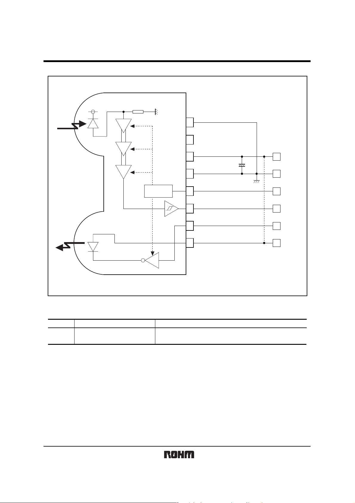
Photo Link Module
zBlock diagram and application circuit
AMP
RPM870-H14
GND
1
NC
234567
Recommended values
Part symbol
C1
Recommended value
1µF, tantalum
Ex.) TCFGA1A105M8R (ROHM)
AMPAMP
V
POWER
DOWN
CC
GND
PWDOWN
RXD
TXD
LEDA
8
C1
V
CC
GND
PWDOWN
RXD
TXD
(LEDV
Notice
Bigger capacitance is recommended with much noise from power supply
CC
)
2/6
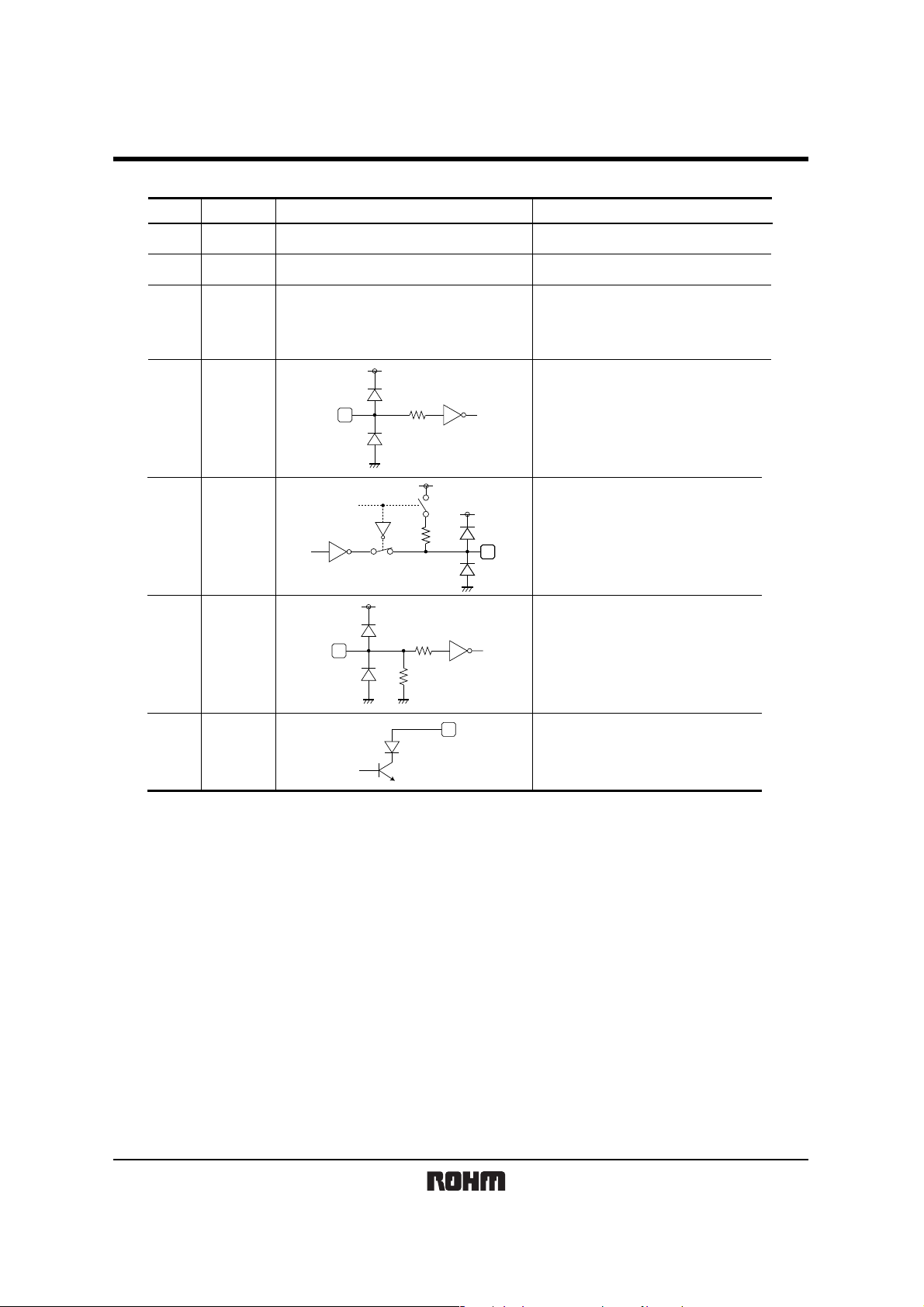
Photo Link Module
zT ermina l description
Circuit Function
V
CC
V
CC
300k
3
5
6
Terminal
CC
V
PWDOWN
RXD
PWDOWN
Pin No
1, 4 GND GND
RPM870-H14
This terminal must be left open.2NC
V
CC
For preventing from ripple noise.
connect a capacitor between
V
CC
(3pin) and GND (4pin).
Power-down control terminal
H : POWERDOWN
L : OPERATION
CMOS logic level input
When input is H, it will stop
the receiving circuit, Pin-PD
current and transmitting LED operation.
V
CC
Receiving data output terminal
CMOS logic level input
When PWDOWN (5pin) = H, the RXD
output will be pulled up to
V
CC
at approximately 300kΩ.
V
CC
7
8
TXD
LEDA
200K
LED
Transmitting data input terminal
H : LED Drive (PWDOWN = L)
CMOS logic level output
Holding TXD = "H"status, LED will
be turn off approximately 48µsec.
LED ANODE terminal
Other power source can be used
difference between LEDV
CC
and VCC.
3/6

Photo Link Module
zElectrical characteristics (Unless otherwise noted, VCC=3V, VL EDVCC=3V , T a=25°C)
Parameter
Consumption Current 1
Consumption Current 2
Transmission rate
PWDOWN INPUT High Voltage
PWDOWN INPUT Low Voltage
PWDOWN INPUT High Current
PWDOWN INPUT Low Current
<Transmitter>
TXD INPUT High Voltage
TXD INPUT Low Voltage
TXD INPUT High Current
TXD INPUT Low Current
LED ANODE Current
<Receiver>
RXD OUTPUT High Voltage
RXD OUTPUT Low Voltage
RXD OUTPUT Rise Time
RXD OUTPUT Fall Time
RXD OUTPUT Pulse Width
Receiver Latency Time
zOptical characteristics (Unless otherwise noted, V
Parameter
Peak wave length
Intensity
Half-Angle
Rise time / Fall time
Optical over shoot
Edge jitter
Irradiance in angular
INPUT Half-Angular
Maximum Emitting Time
1.This product is not designed for protection against radioactive rays.
2.This product dose not include laser transmitter.
3.This product includes one pin photo diode.
4.This product dose not include optical load.
Symbol Min. Typ. Max. Unit Conditions
I
CC
1
I
CC
2
VPDH
VPDL
IPDH
IPDL
VTXH
VTXL
ITXH
ITXL
ILEDA
VRXH
VRXL
tRR
tFR
twRXD
tRT
−
−
2.4
CC
−0.5
V
−
−1.0
−1.0
VCC−0.55
−
7.5
−1.0
−
V
CC
−0.5
−
−
−
1.5
−
90
0.01
15
50
70
30
2.3
100
CC=3V , VLEDVCC=3V, T a=25°C)
120
0.2
−
−
−
0
0
−
−
0
−
−
−
0.55
1.0
1.0
−
0.55
30
1.0
−
−
0.4
−
−
3.6
200
Waiting mode, no input light.
µA
PWDOWN
µA
kbps115.2
V
V
µA
PWDOWN
PWDOWN
µA
V
V
µA
TXD
=
µA
TXD
=
mA
IRXH
V
V
nsec
nsec
µsec
µsec
=
IRXL
=
C
L
=
15pF
C
L
=
15pF
L
=
15pF, 2.4 to 115.2Kbps
C
Symbol Min. Typ. Max. Unit
λP
IE1
θL / 2
Tr / Tf
Tj
Ee
θD / 2
TLEDmax
850
±15
−
−40
0.0068
±15
16
870 nm
104.0
48
900
deg
%25
deg
−15˚ ≤ θL ≤ 15˚
10% to 90%
2
−15˚ ≤ θL ≤ 15˚
TXD=V
mW / sr26
−
−
−
100
nsec
−−
−
500
−
−
−
96
nsec40
mW / cm
µsec
RPM870-H14
=
VCC [V] , no input light.
=
VCC [V]
=
0 [V]
VCC [V]
0 [V]
−50µA
200µA
Conditions
CC
4/6

Photo Link Module
zTiming chart
(Emitting side)
TXD
(7pin)
Internal LED
(Light output)
(Detecting side)
Light input
RXD
(6pin)
less than 48 µsec
more than 48 µsec
(emitting) (emitting) (emitting)
approximately 48 µsec
less than 2.3 µsec more than 2.3 µsec
approximately 2.3 µsecapproximately 2.3 µsec
RPM870-H14
pull up to V
approximately 300kΩ
CC
at
PWDOWN
(5pin)
zNotes
1) LEDV
CC (8pin) and VCC (3pin)
•
Other power source can be used dif ference betw een LEDVCC and VCC.
2) Caution in designing bo ard lay-out
T o get maximum potential from RPM870-H14, please keep in mind following instruction.
•
The line of RXD (6pin) should be connected at backside via through hole close to RPM870-H14 pin lead. Better not
to be close to photo diode side (1pin).
⇒This is to mini mize feedback supplied to photo diode from RXD.
•
As for C1 between 3-4 pin should be placed close to RPM870-H14.
•
Better to be placed more than 1.0cm in radius from photo diode (pin1 side) and also away from the parts which
generates noise, such as DC / DC converter .
3) Others
•
Please be sure to set up the TXD (7pin) input to be “L” (under 0.5V) except transmitting data
(for < 90µsec. on duty < 20%).
•
Powerdown current might increase if exposed by strong light (ex. direct sunlight) at powerdown mode.
•
Please use by the signal format which is specified by IrDA Ver1.2 (Low Power). There might be on error if used by
different signal format.
•
Please pay attention to the lens carefully. Dusts of scratch on the lens may effect the characteristics of product. Please
handle it with care.
4) Eye Safe
•
IEC825-1 (EN60825-1) Class 1 Eye Safe .
5/6

Photo Link Module
zDimensions (Unit : mm)
RPM870-H14
R1.1
2.2
8.0
PinPD
1.0
2.9
0.68±0.1
1.1
1.4
2.8
4.0
A
18
P0.95×7=6.65
0.6 0.48
LED
0.37±0.1
0.95
R1.0
0.15±0.1
2.67
(0.13)
2.2
0.15±0.1
0.78
2.59
0.6±0.1
NOTE
1.TOLERANCE : ±0.2mm
2.COPLANARITY : 0.1mmMAX
UNIT : mm
0.76
A Part Size (Shield Case underside size)
ETH839
2.2
0.75
6/6

Appendix
No technical content pages of this document may be reproduced in any form or transmitted by any
means without prior permission of ROHM CO.,LTD.
The contents described herein are subject to change without notice. The specifications for the
product described in this document are for reference only. Upon actual use, therefore, please request
that specifications to be separately delivered.
Application circuit diagrams and circuit constants contained herein are shown as examples of standard
use and operation. Please pay careful attention to the peripheral conditions when designing circuits
and deciding upon circuit constants in the set.
Any data, including, but not limited to application circuit diagrams information, described herein
are intended only as illustrations of such devices and not as the specifications for such devices. ROHM
CO.,LTD. disclaims any warranty that any use of such devices shall be free from infringement of any
third party's intellectual property rights or other proprietary rights, and further, assumes no liability of
whatsoever nature in the event of any such infringement, or arising from or connected with or related
to the use of such devices.
Upon the sale of any such devices, other than for buyer's right to use such devices itself, resell or
otherwise dispose of the same, no express or implied right or license to practice or commercially
exploit any intellectual property rights or other proprietary rights owned or controlled by
ROHM CO., LTD. is granted to any such buyer.
Products listed in this document are no antiradiation design.
Notes
The products listed in this document are designed to be used with ordinary electronic equipment or devices
(such as audio visual equipment, office-automation equipment, communications devices, electrical
appliances and electronic toys).
Should you intend to use these products with equipment or devices which require an extremely high level of
reliability and the malfunction of with would directly endanger human life (such as medical instruments,
transportation equipment, aerospace machinery, nuclear-reactor controllers, fuel controllers and other
safety devices), please be sure to consult with our sales representative in advance.
About Export Control Order in Japan
Products described herein are the objects of controlled goods in Annex 1 (Item 16) of Export Trade Control
Order in Japan.
In case of export from Japan, please confirm if it applies to "objective" criteria or an "informed" (by MITI clause)
on the basis of "catch all controls for Non-Proliferation of Weapons of Mass Destruction.
Appendix1-Rev1.1
 Loading...