

RPM841-H11
Photo Link Module
IrDA Infrared Communication Module
RPM841-H11
RPM841-H1 1 is an infrared communication module for IrDA V er. 1.2 (Low Power). The infrared LED, PIN photo diode,
LSI are all integrated into a single package. This module is designed with power dow n function and low current
consumption at stand-by mode. The ultra small package makes it a perfect fit for mobile devices.
zFeatures
1) Infrared LED, PIN photo diode, LED driv er & Receiv er freq uency form ation circ uit built in. Impr ovement of EMI noise
protection because of Shield Case.
2) Applied to SIR (2.4 to 115.2kbps)
3) Surface mount type.
4) Power down function built in.
5) Super small package (W=6.8mm, D=2.44mm, H=1.5mm).
6) Infrared remote control transmission driver built-in.
zApplica tions
Mobile phone, PDA, DVC, Digital Still Camera, Printer, Handy Terminal etc.
zAbsolute maximum ratings (Ta=25°C)
Parameter Symbol
in
(3, 4, 5pin)
V
Topr
Tstg
max
−40 to +100
Supply voltage V
Input voltage
Operation temperature
Storage temperature
∗ This applies to all pins basis ground pins (7pin)
zRecommended operating conditions (Ta=25°C)
Parameter Symbol Min. Typ. Max. Unit
Supply voltage
LED supply voltage
CC
V
VLEDV
CC
Limits
∗
7.0
CC
+0.3
−30 to +85
3.0 V2.4 3.6
3.0 V2.6 5.5
Unit
V
V−0.3 to V
°C
°C
1/9
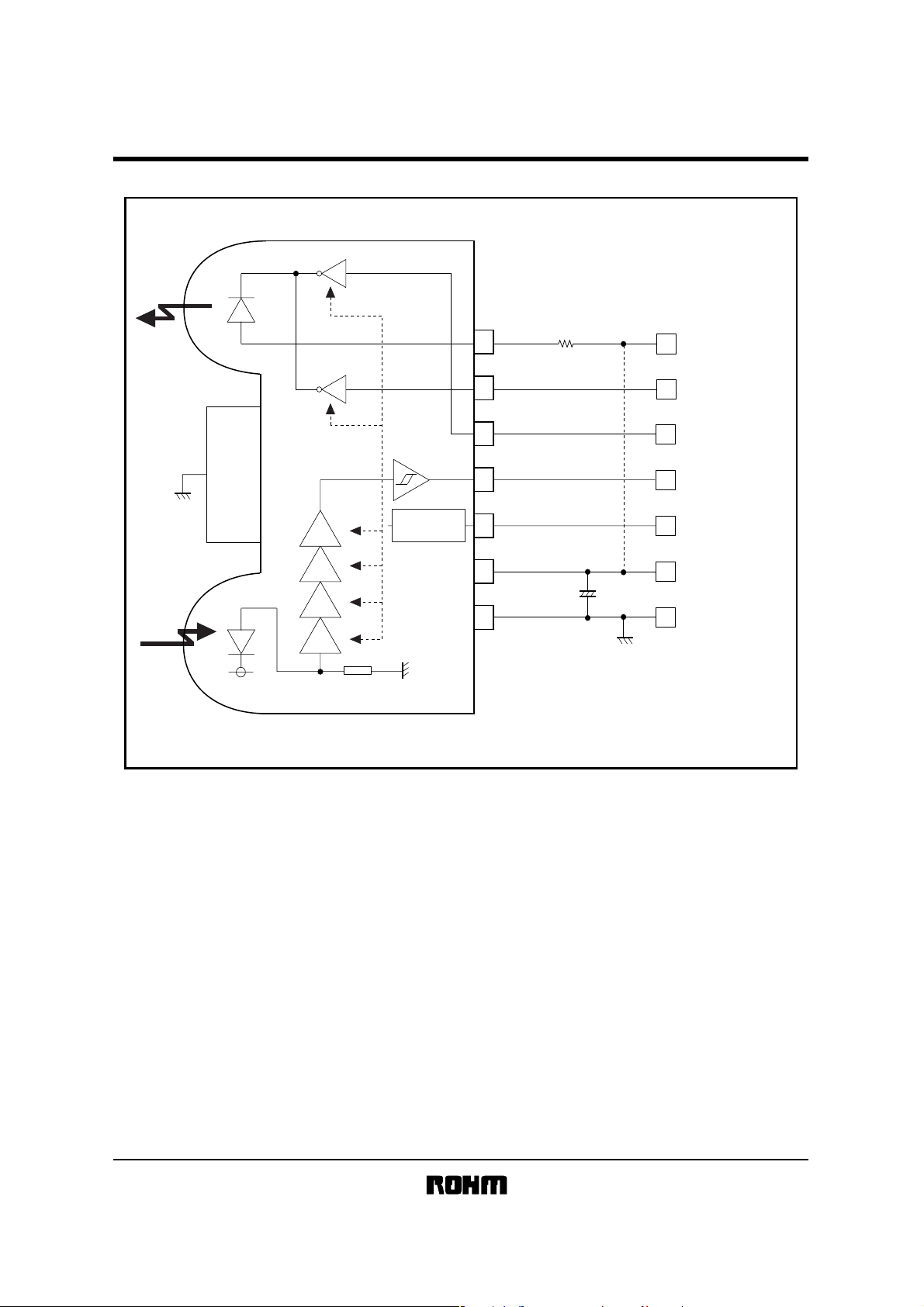
Photo Link Module
zBlock diagram and application circuit
1
2
3
4
LEDA
TX-RC
TXD
RXD
R1
RPM841-H11
CC
)
(LEDV
TX-RC
TXD
RXD
AMP
AMP
AMPAMP
POWER
DOWN
PWDOWN
5
V
CC
6
GND
7
PWDOWN
V
+
C1
VCC (6pin) and LEDVCC (1pin)
can be used on either common power source
or different one
CC
GND
2/9
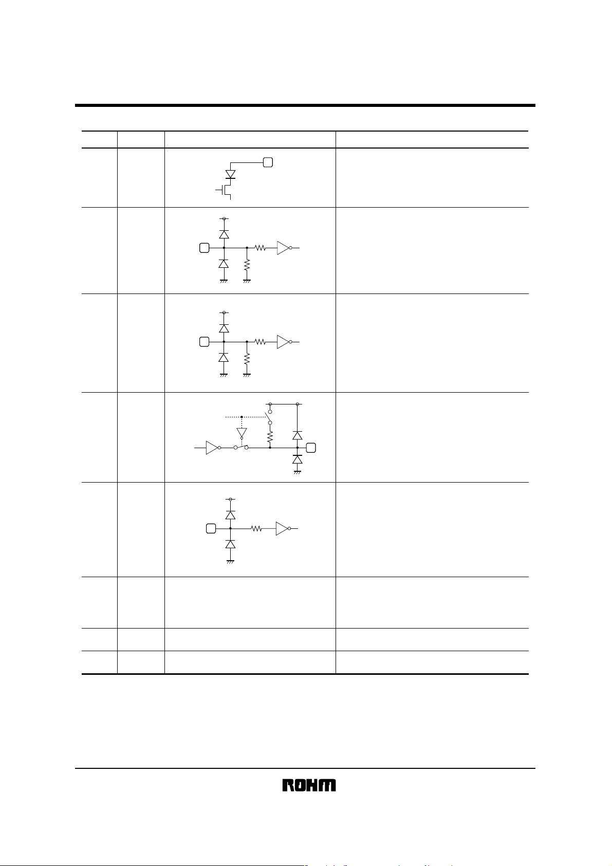
Photo Link Module
zT erminal description
Pin No
Terminal
RPM841-H11
Circuit Function
1
1
LEDA
LED
V
CC
LED ANODE Terminal
Other power source can be used
difference between LEDV
CC and VCC.
RC Transmitting Data Input Terminal
H : LED Emitting (Remote Control Mode)
2
TX-RC
240k
CMOS Logic Level Input
Holding TX-RC='H' status, LED will be
turn off approximately 48µs.
V
CC
Transmitting Data Input Terminal
TXD input at PWDOWN=L
3
TXD
240k
H : LED Emitting
CMOS Logic Level Input
Holding TXD="H" status, LED will be
turn off approximately 48µs.
V
CC
PWDOWN
4
RXD
300k
Receiving Data Output Terminal
CMOS Logic Level Output
When PWDOWN (5pin)= 'H', the RXD
CC
output will be pulled up to V
at
approximately 300kΩ.
V
CC
Power-down Control Terminal
H : POWERDOWN
5
PWDOWN
L : OPERATION
CMOS Logic Level Input
When input is 'H', it will stop the receiving
circuit and Pin-PD current.
Power Supply Terminal
6
V
CC
For preventing from infection, connect
a capacitor between V
CC (6pin) and
GND (7pin).
7
−
GND
Shield Case
Ground Termianl
Connect to Ground.
3/9
Photo Link Module
zElectrical characteristics (Unless otherwise noted, V
Parameter
Consumption current1
Consumption current2
Data rate
PWDOWN input high voltage
PWDOWN input low voltage
PWDOWN input high current
PWDOWN input low current
<Transmitter>
TXD input high voltage
TXD input low voltage
TX-RC input high voltage
TX-RC input low voltage
TXD/TX-RC input high current
TXD/TX-RC input low current
LED anode current (IrDA Mode)
LED anode current (RC Mode)
<Receiver>
RXD output high voltage
RXD output low voltage
RXD output rise Time
RXD output fall Time
RXD output pulse width
Receiver latency time
Symbol Min. Typ. Max. Unit Conditions
I
CC
1
I
CC
2
−
−
2.4
2/3∗V
−1.0
−1.0
2/3∗V
1.5
6.2
−1.0
V
CC
1.7
CC
0
CC
0
0
−
−
−0.4
0
−
−
−
VPDH
VPDL
IPDH
IPDL
VTXH
VTXL
VTX-RCH
VTX-RCL
ITXH
ITXL
ILEDA1
ILEDA2
VRXH
VRXL
tRR
tFR
twRXD
tRT
zOptical characteristics (Unless otherwise noted, V
Parameter
Peak wave length1 (IrDA Mode)
Peak wave length2 (RC Mode)
Optical pulse width1 (IrDA Mode)
Optical pulse width2 (RC Mode)
Rise time / Fall time
Optical over shoot
Edge jitter
Input half-angle
Maximum emitting time
1. This product is not designed for protection against radioactive rays.
2. This product dose not include laser transmitter.
3. This product includes one PIN photo diode.
4. This product dose not include optical load.
Symbol
λP1
λP2
IE1Intensity1 (IrDA Mode) 124 mW/sr28
IE2Intensity2 ( RC Mode) 5025 mW/sr120
θL/2Half-angle −±15 deg−
TWLED1
TWLED2
Tr/Tf
Tj
EeminMinimum Irradiance in angular
EemaxMaximum Irradiance in angular
θD/2
TLEDmax
CC= 3.0V , VLEDVCC=3.0V, Ta=25°C)
Min. Typ. Max. Unit
880
850 900
9.5 10
−40
− 8.1
500 −
±15
20.5
CC= 3.0V , VLEDVCC=3.0V, Ta=25°C)
120
90
0.01
0.2
−
−
V
−
1/3∗V
1.0
0
1.0
0
−
V
1/3∗V
−
−
V
−
0.5
12.5
50
211 mA
25
25
2.6
40
888 nm
25
1.0
0
70
245
−
V
0.4
−
100
100
3.5
200
892
− nm
890880
920
µA
PWDOWN=0V At no input light
µA
PWDOWN=V
kbps115.2
CC
CC
CC
V
VCC=2.4 to 3.6V
CC
V
V
CC
=2.4 to 3.6V
PWDOWN=V
µA
PWDOWN=0V
µA
V
V
CC
=2.4 to 3.6V
CC
V
CC
=2.4 to 3.6V
V
CC
V
V
µA
µA
mA
=2.4 to 3.6V
V
V
CC
=2.4 to 3.6V
TXD=V
CC
or TX-RC=V
TXD=0V or TX-RC=0V
TXD=V
CC
TX-RC=VCC, R1=2.2Ω
V
V
ns
ns
µs
IRXH=
−200µA
IRXL=200µA
C
L
=15pF
C
L
=15pF
C
L
=15pF, 2.4 to 115.2kbps
CC
µs
ILED=50mA, Duty20%
ILED=50mA, Duty20%, −20 to 60°C
nm
ILED=200mA, Duty20%
−15° θL 15° R1=2.2Ω
−15° θL 15° R1=2.2Ω
µs
1.631.42
20−
4.0
48
2.02
10.5
−−
−
µW/cm
−
−
mW/cm
−
96
TXD=1.63µs pulse input R1=2.2Ω
µs
TX-RC=10µs pulse input R
10% to 90%
ns120
%25
ns40
2
−15° θL +15°
2
−15° θL +15°
deg
TXD=0 V
µs
RPM841-H11
CC
At no input light
CC
CC
Conditions
1
CC
or TX-RC=0 V
=2.2Ω
CC
4/9
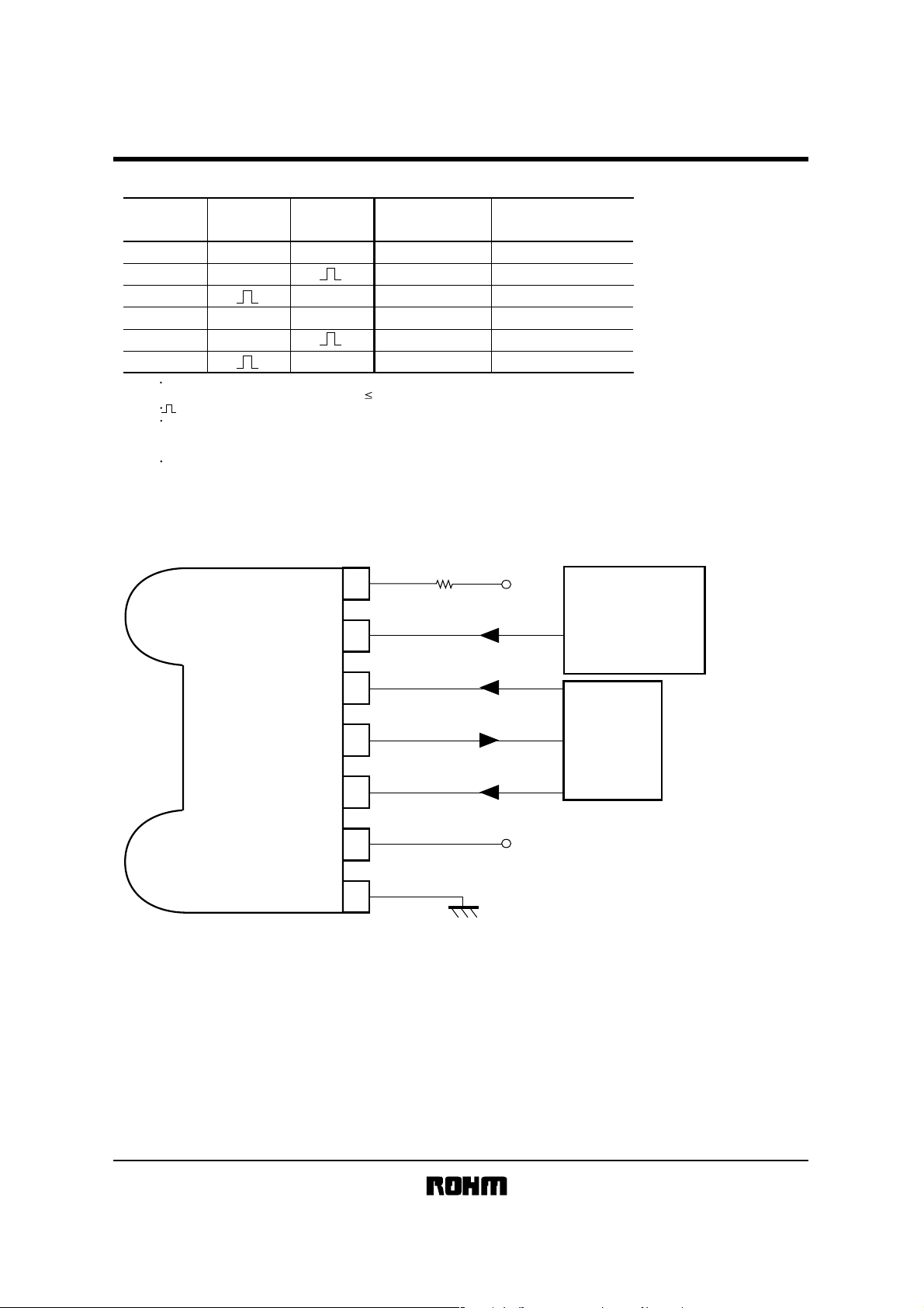
Photo Link Module
zLED Operation Mode Table
PWDOWN
(5pin)
L
L
L
H
H
H
Notes) Please be sure to set up the TX-RC (2pin) and the TXD (3pin) input to be ''L'' (under 0.3V)
except transmitting data (for
of TX-RC (2pin) and TXD (3pin) in the table above is supposed to be the pulse input.
When either TX-RC (2pin) input TXD (3pin) input keeps the state of ''H'' (more than appproximately 48µs),
LED will be turned off due to LED pulse width limiting circuit if the pulse is input from the other terminal.
Therefore, don't use as the normal transmitting is impossible.
Please input the pulse when both TX-RC (2pin) and TXD (3pin) are ''L''.
TX-RC
(4pin)
L
L
L
L
TXD
(7pin)
L
L
L
L
<
90µs. ON Duty 50%).
LED
Emitting Mode
OFF
IrDA
RC
OFF
OFF
RC
IrDA Receiver
Operation Condition
zInterface operating timing
(Emitting side)
(1) When TXD output for IrDA and TXD output for controller are different lines.
1
LEDA
TX-RC
LEDV
RPM841-H11
ON
ON
ON
OFF
OFF
OFF
CC
RC Transmitting
Controller
(BU787X etc)
TXD
RXD
IrDA
Controller
PWDOWN
V
CC
GND
V
CC
7
5/9

Photo Link Module
(2-a) RC transmitting mode at IrDA receiver active condition.
Input Condition
TX-RC
(2pin)
TXD
(3pin)
PWDOWN
(5pin)
PWDOWN
L
L
L
H
TX-RC LED Mode
L
L
L
Min 1µs
TXD
L
L
L
OFF
IrDA
RC
OFF
RPM841-H11
Recriver circuit
ON
ON
ON
OFF
Min 1µs
LED Emitting
Emitting Mode
∗
If TX-RC or TXD input pulse width is wider than 48µs, output LED emitting pulse will be turn off approximately 48µs.
IrDA IrDARC RC
6/9
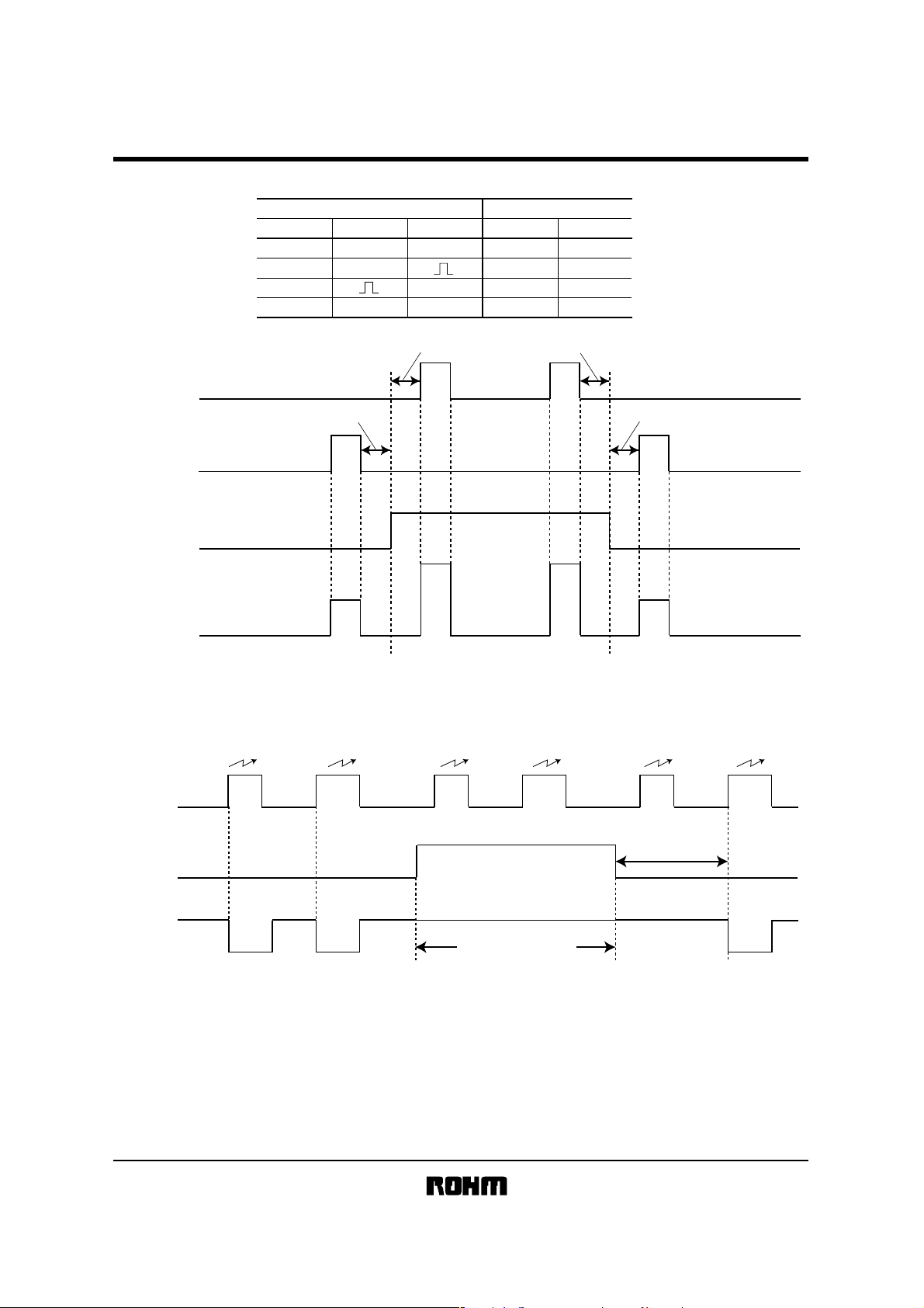
Photo Link Module
(2-b) RC transmit mode at IrDA receiver power dow n condition.
Input Condition
PWDOWN
L
L
H
H
TX-RC LED Mode
L
L
L
TXD
L
L
L
OFF
IrDA
RC
OFF
RPM841-H11
Recriver circuit
ON
ON
OFF
OFF
Min 1µs
TX-RC
(2pin)
TXD
(3pin)
PWDOWN
(5pin)
LED Emitting
Emitting Mode
∗
If TX-RC or TXD input pulse width is wider than 48µs, output LED emitting pulse will be turn off approximately 48µs.
Min 1µs
IrDA IrDARC RC
Min 1µs
Min 1µs
(Receiving side)
Light input
Min 200µs
PWDOWN
(5pin)
RXD
(4pin)
∗
RXD output width is fixed approximately 2.6µs.
Note RXD output become stable after 200µs since PWDOWN is changed from H to L.
RXD output could be unstable at H to L within 200µs.
Pull up to VCC at
approximately 300kΩ
7/9

RPM841-H11
Photo Link Module
zAtt ached compone nts
Recommended values
Part symbol
C1
R1
[LED current set-up method for Remote control mode]
In case of using R1 with different condition from the above, formula is as follows :
LED resistance value : R1[Ω], LED average consumption current : ILED[mA], Supply voltage : VLEDV
minimum necessary of irradiant intensity le1 [mW / sr]
(Including LED’s distribution within ±15deg)
R1=166 × (VLEDV
ILED=Duty × (VLEDVCC−1.31) / (R1+5.8)
Duty : LED duty at emitting
∗ Please set up to be ILED / Duty < 250[mA] (Duty ≤ 25%)
∗ At IrDA Mode, LED current is constantly approximately 50mA.
(Reference) In case of using R1, typical intensity (le1typ) and maximum intensity (le1max) on
le1typ=280 × (VLEDV
le1max=560 × (VLEDV
zNotes
1) LEDV
•
Other power source can be used difference between LEDVCC and VCC.
2) Caution in designing board lay-out
T o get maximum potential from RPM841-H11, please keep in mind following instruction.
•
The line of RXD (4pin) should be connected at backside via through hole close to RPM841-H11 pin lead. Better not to
be close to photo diode side (7pin).
⇒This is to minimize feedback supplied to photo diode from RXD.
•
As for C1 between 6-7 pin should be placed close to RPM841-H1 1.
•
Better to be placed more than 1.0cm in radius from photo diode (pin7 side) and also away from the parts w hich
generates noise, such as DC
3) Notes
•
Please be sure to set up the TX-RC (2pin) and the TXD (3pin) input to be “L” (under 0.3V) except transmitting data
(for < 90µs, ON duty ≤ 50%).
•
Power down current might increase if exposed by strong light (ex. direct sunlight) at pow erdow n mode.
•
Please use by the signal format at IrDA operating mode w hich is specified by IrDA Ver1.2 (2.4k to 115.2kbps). There
might be on error if used by different signal format.
•
Please pay attention to the lens carefully.
Dusts of scratch on the lens may effect the characteristics of product. Please handle it with care.
1µF, tantalum or ceramic
Ex.) TCFGA1A105M8R (ROHM)
2.2Ω±5%, 1/8W
(VLEDV
CC−1.31) / le1−7.2
axis are described as below.
CC (1pin), VCC (6pin)
Recommended value
CC
=3V)
CC−1.31) / (R1+5.8)
CC−1.31) / (R1+5.8)
/
DC converter.
Notice
Bigger capacitance is recommended with much noise from power supply
At LED Emitting Duty=25%
CC[V],
8/9

Photo Link Module
4) Eye safe
•
IEC60825-1 (IEC60825-1 amendment2), Class 1 Eye Safe.
5) LED current derating and amdient temperature
The relation between LED peak current and maximum ambient temperature is shown below.
We recommend you to use within the range as indicated in below .
When glass-epoxy board (50×50×1.6mm) mounted.
300
250
RPM841-H11
200
150
100
50
0
−200 2040608010
MAXIMUM LED PEAK CURRENT : Iledp (mA)
Duty:25%
Duty:20%
Duty:15%
Duty:10%
AMBIENT TEMPERATURE : Ta
(°C)
zExternal dimensions (Unit : mm)
RPM841-H11
6.8
3.4
R0.83
1.5
2.38
LED
0.68
2.16
1.1
6.4
0
PD
R0.9
2.18
0.1
±
0.1
2.44
2.09
0.16
0.37±0.1
0.95
P0.95×6=5.7
0.4
7pin1pin
NOTE
1.TOLERANCE:
±
0.2
UNIT:mm
ETH774
9/9
Appendix
No technical content pages of this document may be reproduced in any form or transmitted by any
means without prior permission of ROHM CO.,LTD.
The contents described herein are subject to change without notice. The specifications for the
product described in this document are for reference only. Upon actual use, therefore, please request
that specifications to be separately delivered.
Application circuit diagrams and circuit constants contained herein are shown as examples of standard
use and operation. Please pay careful attention to the peripheral conditions when designing circuits
and deciding upon circuit constants in the set.
Any data, including, but not limited to application circuit diagrams information, described herein
are intended only as illustrations of such devices and not as the specifications for such devices. ROHM
CO.,LTD. disclaims any warranty that any use of such devices shall be free from infringement of any
third party's intellectual property rights or other proprietary rights, and further, assumes no liability of
whatsoever nature in the event of any such infringement, or arising from or connected with or related
to the use of such devices.
Upon the sale of any such devices, other than for buyer's right to use such devices itself, resell or
otherwise dispose of the same, no express or implied right or license to practice or commercially
exploit any intellectual property rights or other proprietary rights owned or controlled by
ROHM CO., LTD. is granted to any such buyer.
Products listed in this document are no antiradiation design.
Notes
The products listed in this document are designed to be used with ordinary electronic equipment or devices
(such as audio visual equipment, office-automation equipment, communications devices, electrical
appliances and electronic toys).
Should you intend to use these products with equipment or devices which require an extremely high level of
reliability and the malfunction of with would directly endanger human life (such as medical instruments,
transportation equipment, aerospace machinery, nuclear-reactor controllers, fuel controllers and other
safety devices), please be sure to consult with our sales representative in advance.
About Export Control Order in Japan
Products described herein are the objects of controlled goods in Annex 1 (Item 16) of Export Trade Control
Order in Japan.
In case of export from Japan, please confirm if it applies to "objective" criteria or an "informed" (by MITI clause)
on the basis of "catch all controls for Non-Proliferation of Weapons of Mass Destruction.
Appendix1-Rev1.1
 Loading...