

Datasheet
www.rohm.com
© 2012 ROHM Co., Ltd. All rights reserved.
R6006ANX
Nch 600V 6A Power MOSFET
mJ
Junction temperature
30
E
AR
*4
Avalanche energy, single pulse
Avalanche energy, repetitive
Avalanche current
3A1.9
EAS
*3
mJ
V
Gate - Source voltage
P
D
40
I
D,pulse
*2
I
D
*1
2.9
AAV/ns
150
Reverse diode dv/dt
I
AR
*3
Range of storage temperature
T
stg
Power dissipation (Tc = 25C)
CWC
dv/dt
*5
15
-55 to +150
T
j
500
Symbol
Taping code
lAbsolute maximum ratings (Ta = 25C)
-
Marking
R6006ANX
Parameter
Tape width (mm)
-
lApplication
Bulk
-
Type
Packing
6
Reel size (mm)
Value
V
Unit
600
V
DSS
I
D
*1
A
Tc = 25C
Drain - Source voltage
lFeatures
V
DSS
2.4
V
GSS
24
Continuous drain current
Basic ordering unit (pcs)
Pulsed drain current
40W
6A
5) Parallel use is easy.
Tc = 100C
Switching Power Supply
4) Drive circuits can be simple.
2) Fast switching speed.
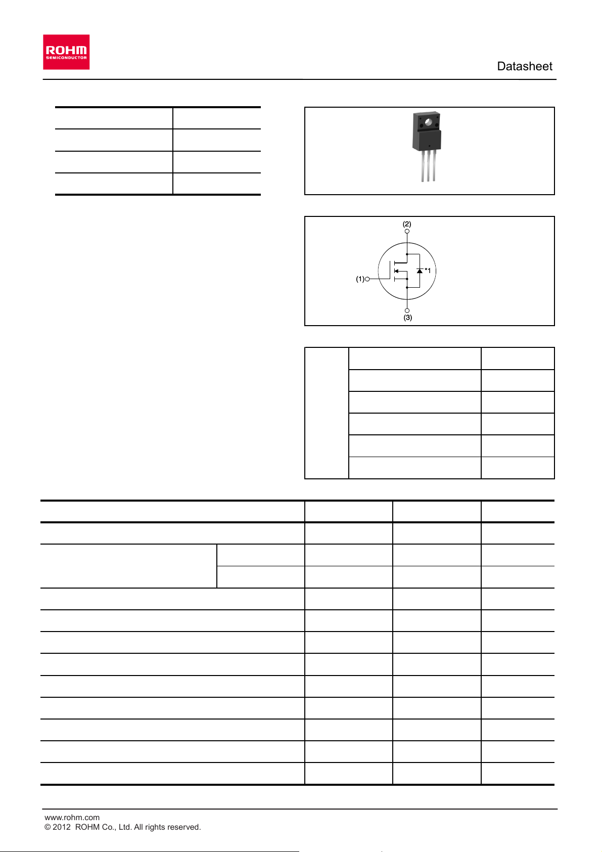
lOutline
lInner circuit
lPackaging specifications
TO-220FM
600V
1.2W
R
DS(on)
(Max.)
IDP
D
1) Low on-resistance.
6) Pb-free lead plating ; RoHS compliant
3) Gate-source voltage (V
GSS
) guaranteed to be 30V.
(1) Gate
(2) Drain
(3) Source
*1 Body Diode
(1)
(2)
(3)
1/13
2012.01 - Rev.B

www.rohm.com
© 2012 ROHM Co., Ltd. All rights reserved.
Data Sheet
R6006ANX
W
Gate input resistance
R
G
f = 1MHz, open drain
-
7.6
-
Static drain - source
on - state resistance
W
Tj = 25C
-
0.9
1.2
Tj = 125°C
-
R
DS(on)
*6
V
GS
= 10V, ID = 3A
1.9
-
Unit
Max.
-
700
-
-
70
Gate threshold voltage
V
GS (th)
V
DS
= 10V, ID = 1mA
2.5
Gate - Source leakage current
V
GS
= 30V, V
DS
= 0V
--V
4.5
Thermal resistance, junction - ambient
Soldering temperature, wavesoldering for 10s
lElectrical characteristics (Ta = 25C)
Parameter
Drain - Source breakdown
voltage
V
DS
= 600V, V
GS
= 0V
Unit
T
soldRthJA
Min.
R
thJC
Symbol
-
Unit
C/W
Values
V/ns
Tj = 125C
50
-
3.125
-
C
-
265
C/W
Drain - Source avalanche
breakdown voltage
-
600
Conditions
Symbol
V
(BR)DS
-
Min.
Values
Typ.
100
-
Zero gate voltage
drain current
V
(BR)DSS
V
GS
= 0V, ID = 6A
V
GS
= 0V, ID = 1mA
I
DSS
I
GSS
-
nA
Tj = 125°C
V
V
0.1mA1000
100
-
-
T
j
= 25C
Drain - Source voltage slope
dv/dt
VDS = 480V, ID = 6A
-
Typ.
Symbol
Conditions
Values
lAbsolute maximum ratings
lThermal resistance
Thermal resistance, junction - case
Parameter
Max.
Parameter
2/13
2012.01 - Rev.B

www.rohm.com
© 2012 ROHM Co., Ltd. All rights reserved.
Data Sheet
R6006ANX
*1 Limited only by maximum temperature allowed.
*2 PW 10ms, Duty cycle 1%
*3 L ⋍ 500mH, V
DD
= 50V, RG = 25W, starting Tj = 25C
*4 L ⋍ 500mH, V
DD
= 50V, RG = 25W, starting Tj = 25C, f = 10kHz
*5 Reference measurement circuits Fig.5-1.
*6 Pulsed
Max.
Reverse transfer capacitance
lElectrical characteristics (Ta = 25C)
Parameter
Symbol
Conditions
Values
Unit
Min.
Typ.
3.5
Transconductance
Input capacitance
1.7
Output capacitance
C
oss
V
DS
= 25V
--S
C
iss
V
GS
= 0V
-
520
-
g
fs
*6
V
DS
= 10V, ID = 3.0A
pF
-
C
rss
f = 1MHz
-25-
380
pF
-25-
-
25
Turn - on delay time
t
d(on)
*6
V
DD
⋍ 300V, V
GS
= 10V
-
Effective output capacitance,
energy related
Effective output capacitance,
time related
C
o(er)
C
o(tr)
V
GS
= 0V
V
DS
= 0V to 480V
22
RG = 10W
-
Turn - off delay time
t
d(off)
*6
RL = 100W
-
Fall time
t
f
*6
-
-
Typ.ns50
1003570--
Max.
Unit
nC
-
Parameter
lGate Charge characteristics (Ta = 25C)
Rise time
t
r
*6
ID = 3A
Symbol
Values
18
VGS = 10V
-4-
Min.15-
Conditions
Total gate charge
Gate - Source charge
Q
gs
*6
ID = 6A
Q
g
*6
V
DD
⋍ 300V
6-6.0-V
Gate plateau voltage
V
(plateau)
V
DD
⋍ 300V, ID = 6A
-
-
Gate - Drain charge
Q
gd
*6
3/13
2012.01 - Rev.B
www.rohm.com
© 2012 ROHM Co., Ltd. All rights reserved.
Data Sheet
R6006ANX
Unit
-AA
1.5
V
ns
24
6
Peak rate of fall of reverse
recovery current
dirr/dt
-
Value
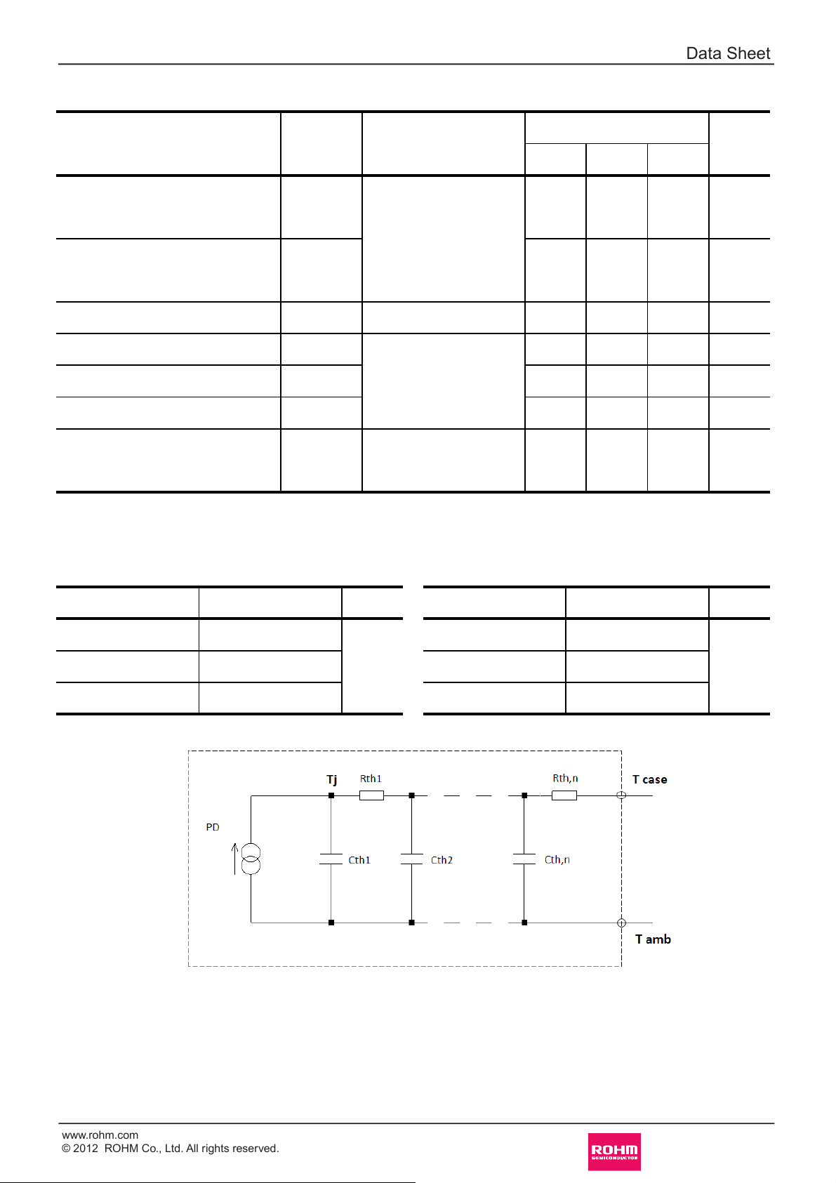
lTypical Transient Thermal Characteristics
300
-
Symbol
Value
Unit
Symbol
-
A
A/ms
-
Tj = 25C
0.00138
K/W
Ws/K
R
th2
1.15
C
th2
0.0146
0.342
C
th1Rth1Rth3
2.19
C
th3
0.452
IS = 6A
di/dt = 100A/ms
302
---
lBody diode electrical characteristics (Source-Drain) (Ta = 25C)
-
2.0
-
mC
V
SD
*6
V
GS
= 0V, IS = 6A
Typ.
Forward voltage
Reverse recovery time
Unit
Min.
Max.
Inverse diode continuous,
forward current
Inverse diode direct current,
pulsed
-
Peak reverse recovery current
Parameter
Symbol
Conditions
Values
Reverse recovery charge
t
rr
*6
-
-13-
Q
rr
*6
I
rrm
*6
IS *1ISM
*2
Tc = 25C
4/13
2012.01 - Rev.B
www.rohm.com
© 2012 ROHM Co., Ltd. All rights reserved.
Data Sheet
R6006ANX
lElectrical characteristic curves
0
20
40
60
80
100
120
0 50 100 150 200
0.0001
0.001
0.01
0.1
1
10
100
1000
0.0001 0.01 1 100
T
a
= 25ºC
Single Pulse
R
th(ch-a)(t)
= r
(t)
×Rth(ch-
a)
Rth(ch-a) = 70ºC/W
top D = 1
D = 0.5
D = 0.1
D = 0.05
D = 0.01
D = Single
Fig.1 Power Dissipation Derating Curve
Power Dissipation : P
D
/P
D
max. [%]
Junction Temperature : Tj [°C]
Fig.2 Maximum Safe Operating Area
Drain Current : I
D
[A]
Drain - Source Voltage : VDS [V]
Fig.3 Normalized Transient Thermal
Resistance vs. Pulse Width
Normalized Transient Thermal Resistance : r
(t)
Pulse Width : PW [s]
0.01
0.1
1
10
100
0.1 1 10 100 1000
T
a
= 25ºC
Single Pulse
Operation in this
area is limited
by R
DS(ON)
PW = 100us
PW = 1ms
PW = 10ms
5/13
2012.01 - Rev.B
www.rohm.com
© 2012 ROHM Co., Ltd. All rights reserved.
Data Sheet
R6006ANX
lElectrical characteristic curves
0
1
2
3
4
0.01 0.1 1 10 100
Ta = 25ºC
VDD=50V,RG=25Ω
VGF=10V,VGR=0V
0
20
40
60
80
100
120
0 25 50 75 100 125 150 175
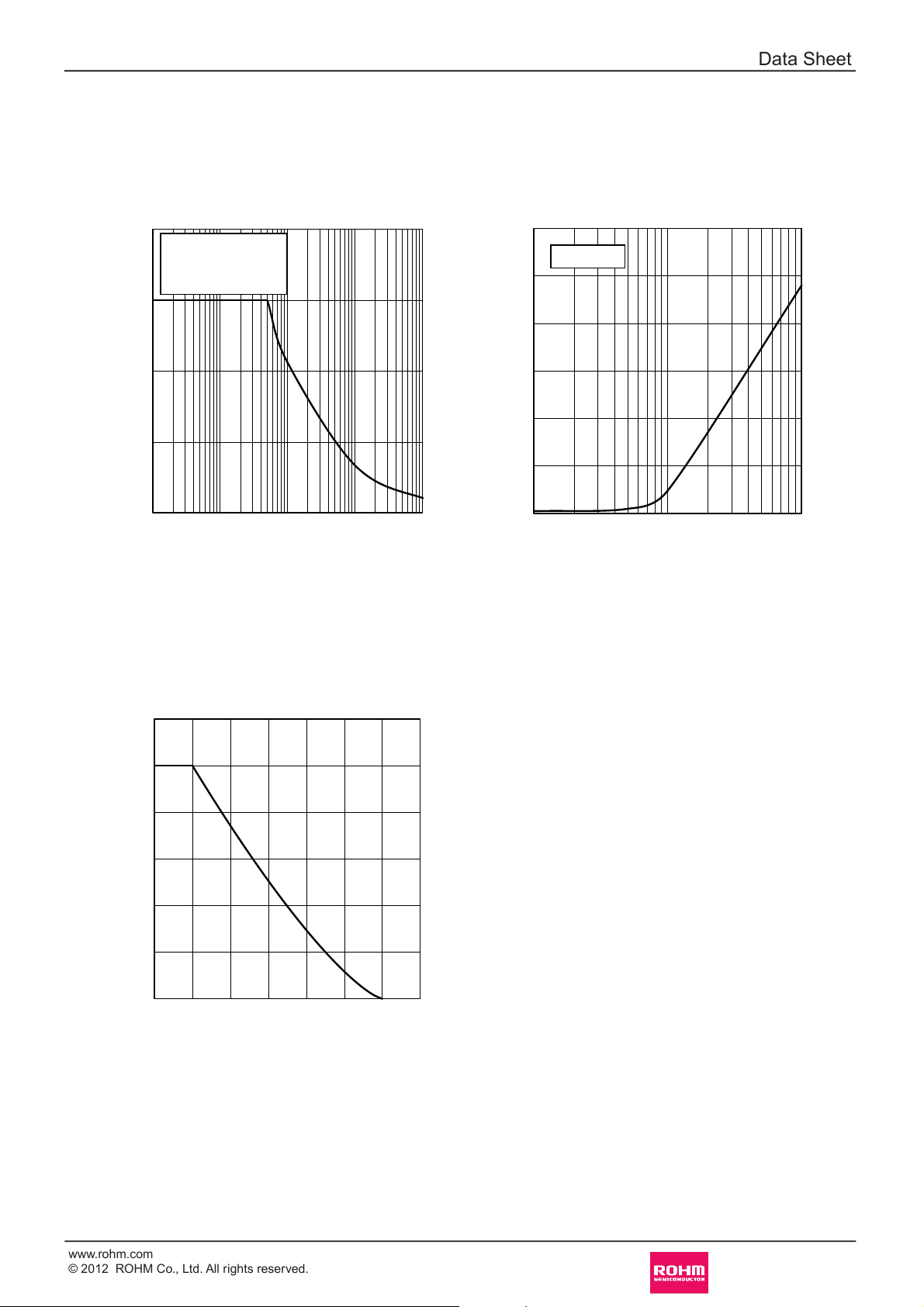
Fig.4 Avalanche Current vs Inductive Load
Avalanche Current : I
AR
[A]
Coil Inductance : L [mH]
Fig.5 Avalanche Power Losses
Avalanche Power Losses : P
AR
[W]
Frequency : f [Hz]
Fig.6 Avalanche Energy Derating Curve
vs Junction Temperature
Avalanche Energy : E
AS
/ E
AS
max. [%]
Junction Temperature : Tj [ºC]
0
500
1000
1500
2000
2500
3000
1.0E+04 1.0E+05 1.0E+06
Ta = 25ºC
6/13
2012.01 - Rev.B
www.rohm.com
© 2012 ROHM Co., Ltd. All rights reserved.
Data Sheet
R6006ANX
lElectrical characteristic curves
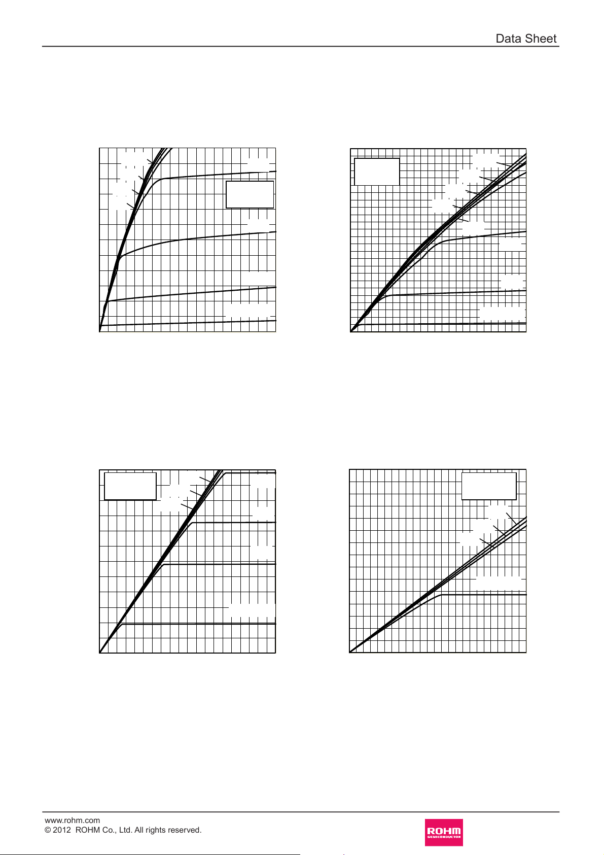
Fig.7 Typical Output Characteristics(I)
Drain Current : I
D
[A]
Drain - Source Voltage : VDS [V]
Fig.8 Typical Output Characteristics(II)
Drain Current : I
D
[A]
Drain - Source Voltage : VDS [V]
Fig.9 Tj = 150°C Typical Output
Characteristics(I)
Drain Current : I
D
[A]
Drain - Source Voltage : VDS [V]
Fig.10 Tj = 150°C Typical Output
Characteristics(II)
Drain Current : I
D
[A]
Drain - Source Voltage : VDS [V]
0
1
2
3
4
5
6
0 5 10 15 20
T
a
= 25ºC
Pulsed
5.0V
VGS= 4.5V
6.0V
7.0V
6.5V
10.0V
5.5V
8.0V
0
1
2
3
4
5
0 1 2 3 4 5
Ta = 25ºC
Pulsed
VGS= 4.5V
5.0V
6.0V
5.5V
6.5V
7.0V
8.0V
10.0V
0
1
2
3
4
5
6
0 5 10 15 20
Ta = 150ºC
Pulsed
5.5V
V
GS
= 4.5V
6.5V
10V
6.0V
7.0V
8.0V
0
1
2
3
0 1 2 3 4 5
Ta = 150ºC
Pulsed
VGS= 4.5V
10V
6.5V
5.5V
7/13
2012.01 - Rev.B

www.rohm.com
© 2012 ROHM Co., Ltd. All rights reserved.
Data Sheet
R6006ANX
lElectrical characteristic curves
500
550
600
650
700
750
800
850
900
-50 0 50 100 150
0.001
0.01
0.1
1
10
100
0 2 4 6 8
V
DS
= 10V
Pulsed
T
a
= 125ºC
T
a
= 75ºC
T
a
= 25ºC
Ta = -25ºC
0
1
2
3
4
5
6
-50 0 50 100 150
V
DS
= 10V
ID = 1mA
0.001
0.01
0.1
1
10
100
0.001 0.01 0.1 1 10
V
DS
= 10V
Pulsed
T
a
= -25ºC
T
a
= 25ºC
T
a
= 75ºC
Ta = 125ºC
Fig.11 Breakdown Voltage
vs. Junction Temperature
Drain - Source Breakdown Voltage : V
(BR)DSS
[V]
Junction Temperature : Tj [°C]
Fig.12 Typical Transfer Characteristics
Drain Current : I
D
[A]
Gate - Source Voltage : VGS [V]
Fig.13 Gate Threshold Voltage
vs. Junction Temperature
Gate Threshold Voltage : V
GS(th)
[V]
Junction Temperature : Tj [°C]
Fig.14 Transconductance vs. Drain Current
Transconductance : g
fs
[S]
Drain Current : ID [A]
8/13
2012.01 - Rev.B

www.rohm.com
© 2012 ROHM Co., Ltd. All rights reserved.
Data Sheet
R6006ANX
lElectrical characteristic curves
0
0.5
1
1.5
2
2.5
3
0 5 10 15
Ta = 25ºC
Pulsed
ID = 3.0A
ID = 6.0A
0
0.5
1
1.5
2
2.5
3
-50 0 50 100 150
V
GS
= 10V
Pulsed
ID= 3.0A
ID= 6.0A
0
1
10
0.001 0.01 0.1 1 10 100
V
GS
= 10V
Pulsed
T
a
= 125ºC
T
a
= 75ºC
T
a
= 25ºC
Ta = -25ºC
Fig.15 Static Drain - Source On - State
Resistance vs. Gate Source Voltage
Static Drain - Source On-State Resistance
: R
DS(on)
[Ω]
Gate - Source Voltage : VGS [V]
Fig.16 Static Drain - Source On - State
Resistance vs. Junction Temperature
Static Drain - Source On-State Resistance
: R
DS(on)
[Ω]
Junction Temperature : Tj [ºC]
Fig.17 Static Drain - Source On - State
Resistance vs. Drain Current
Static Drain - Source On-State Resistance
: R
DS(on)
[Ω]
Drain Current : ID [A]
9/13
2012.01 - Rev.B

www.rohm.com
© 2012 ROHM Co., Ltd. All rights reserved.
Data Sheet
R6006ANX
lElectrical characteristic curves
0.0
2.0
4.0
0 200 400 600
Ta = 25ºC
1
10
100
1000
10000
0.1 1 10 100 1000
C
iss
C
oss
C
rss
T
a
= 25ºC
f = 1MHz
V
GS
= 0V
1
10
100
1000
10000
0.01 0.1 1 10 100
T
a
= 25ºC
V
DD
⋍
300V
V
GS
= 10V
R
G
= 10Ω
Pulsed
t
d(on)
t
r
t
d(off) tf
0
5
10
0 5 10 15 20
T
a
= 25ºC
V
DD
⋍
300V
I
D
= 6A
R
G
= 10Ω
Pulsed
Fig.18 Typical Capacitance
vs. Drain - Source Voltage
Capacitance : C [pF]
Drain - Source Voltage : VDS [V]
Fig.19 Coss Stored Energy
Coss Stored Energy : E
OSS
[uJ]
Drain - Source Voltage : VDS [V]
Fig.20 Switching Characteristics
Switching Time : t [ns]
Drain Current : ID [A]
Fig.21 Dynamic Input Characteristics
Gate - Source Voltage : V
GS
[V]
Total Gate Charge : Qg [nC]
10/13
2012.01 - Rev.B
www.rohm.com
© 2012 ROHM Co., Ltd. All rights reserved.
Data Sheet
R6006ANX
lElectrical characteristic curves
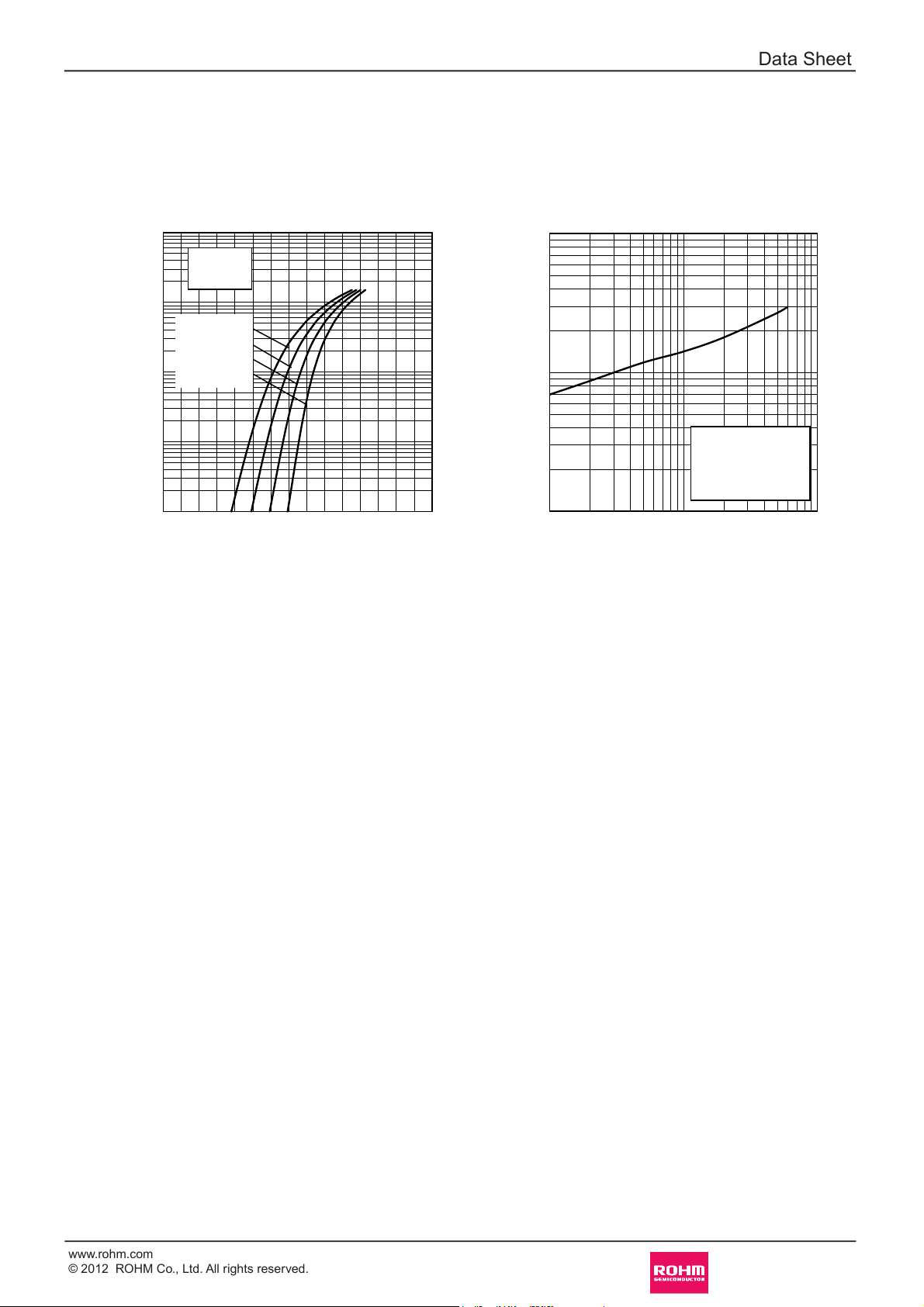
0.01
0.1
1
10
100
0 0.5 1 1.5
V
GS
= 0V
Pulsed
T
a
= 125ºC
Ta
= 75ºC
Ta
= 25ºC
Ta = -25ºC
10
100
1000
0.1 1 10
T
a
= 25ºC
di / dt = 100A / μs
V
GS
= 0V
Pulsed
Fig.22 Inverse Diode Forward Current
vs. Source - Drain Voltage
Inverse Diode Forward Current : I
S
[A]
Source - Drain Voltage : VSD [V]
Fig.23 Reverse Recovery Time
vs.Inverse Diode Forward Current
Reverse Recovery Time : t
rr
[ns]
Inverse Diode Forward Current : IS [A]
11/13
2012.01 - Rev.B

www.rohm.com
© 2012 ROHM Co., Ltd. All rights reserved.
Data Sheet
R6006ANX
lMeasurement circuits
Fig.1-1 Switching Time Measurement Circuit
Fig.1-2 Switching Waveforms
Fig.2-1 Gate Charge Measurement Circuit
Fig.2-2 Gate Charge Waveform
Fig.3-1 Avalanche Measurement Circuit Fig.3-2 Avalanche Waveform
Fig.4-1 dv/dt Measurement Circuit Fig.4-2 dv/dt Waveform
Fig.5-1 di/dt Measurement Circuit Fig.5-2 di/dt Waveform
12/13
2012.01 - Rev.B

www.rohm.com
© 2012 ROHM Co., Ltd. All rights reserved.
Data Sheet
R6006ANX
lDimensions (Unit : mm)
Dimension in mm/inches
D
b1
E1
E
e
b
c
F
A2A1
AL
x A
A4
φ
p
Q
A
TO-220FM
MIN MAX MIN MAX
A 16.60 17.60 0.654 0.693
A1 1.80 2.20 0.071 0.087
A2 14.80 15.40 0.583 0.606
A4 6.80 7.20 0.268 0.283
b 0.70 0.85 0.028 0.033
b1 1.10 1.50 0.043 0.059
c 0.70 0.85 0.028 0.033
D 9.90 10.30 0.39 0.406
E 4.40 4.80 0.173 0.189
e
E1 2.70 3.00 0.106 0.118
F 2.80 3.20 0.11 0.126
L 11.50 12.50 0.453 0.492
p 3.00 3.40 0.118 0.134
Q 2.10 3.10 0.083 0.122
x - 0.381 - 0.015
2.54
0.10
DIM
MILIMETERS
INCHES
13/13
2012.01 - Rev.B

Notes
No copying or reproduction of this document, in part or in whole, is permitted without the
consent of ROHM Co.,Ltd.
The content specied herein is subject to change for improvement without notice.
The content specied herein is for the purpose of introducing ROHM's products (hereinafter
"Products"). If you wish to use any such Product, please be sure to refer to the specications,
which can be obtained from ROHM upon request.
Examples of application circuits, circuit constants and any other information contained herein
illustrate the standard usage and operations of the Products. The peripheral conditions must
be taken into account when designing circuits for mass production.
Great care was taken in ensuring the accuracy of the information specied in this document.
However, should you incur any damage arising from any inaccuracy or misprint of such
information, ROHM shall bear no responsibility for such damage.
The technical information specied herein is intended only to show the typical functions of and
examples of application circuits for the Products. ROHM does not grant you, explicitly or
implicitly, any license to use or exercise intellectual property or other rights held by ROHM and
other parties. ROHM shall bear no responsibility whatsoever for any dispute arising from the
use of such technical information.
The Products specied in this document are intended to be used with general-use electronic
equipment or devices (such as audio visual equipment, ofce-automation equipment, communication devices, electronic appliances and amusement devices).
The Products specied in this document are not designed to be radiation tolerant.
While ROHM always makes efforts to enhance the quality and reliability of its Products, a
Product may fail or malfunction for a variety of reasons.
Please be sure to implement in your equipment using the Products safety measures to guard
against the possibility of physical injury, re or any other damage caused in the event of the
failure of any Product, such as derating, redundancy, re control and fail-safe designs. ROHM
shall bear no responsibility whatsoever for your use of any Product outside of the prescribed
scope or not in accordance with the instruction manual.
The Products are not designed or manufactured to be used with any equipment, device or
system which requires an extremely high level of reliability the failure or malfunction of which
may result in a direct threat to human life or create a risk of human injur y (such as a medical
instrument, transportation equipment, aerospace machinery, nuclear-reactor controller, fuelcontroller or other safety device). ROHM shall bear no responsibility in any way for use of any
of the Products for the above special purposes. If a Product is intended to be used for any
such special purpose, please contact a ROHM sales representative before purchasing.
If you intend to export or ship overseas any Product or technology specied herein that may
be controlled under the Foreign Exchange and the Foreign Trade Law, you will be required to
obtain a license or permit under the Law.
Notice
Thank you for your accessing to ROHM product informations.
More detail product informations and catalogs are available, please contact us.
ROHM Customer Support System
www.rohm.com
© 2012 ROHM Co., Ltd. All rights reserved.
http://www.rohm.com/contact/
R1120A
 Loading...