

C
10V Drive Nch MOSFET
R5005CNX
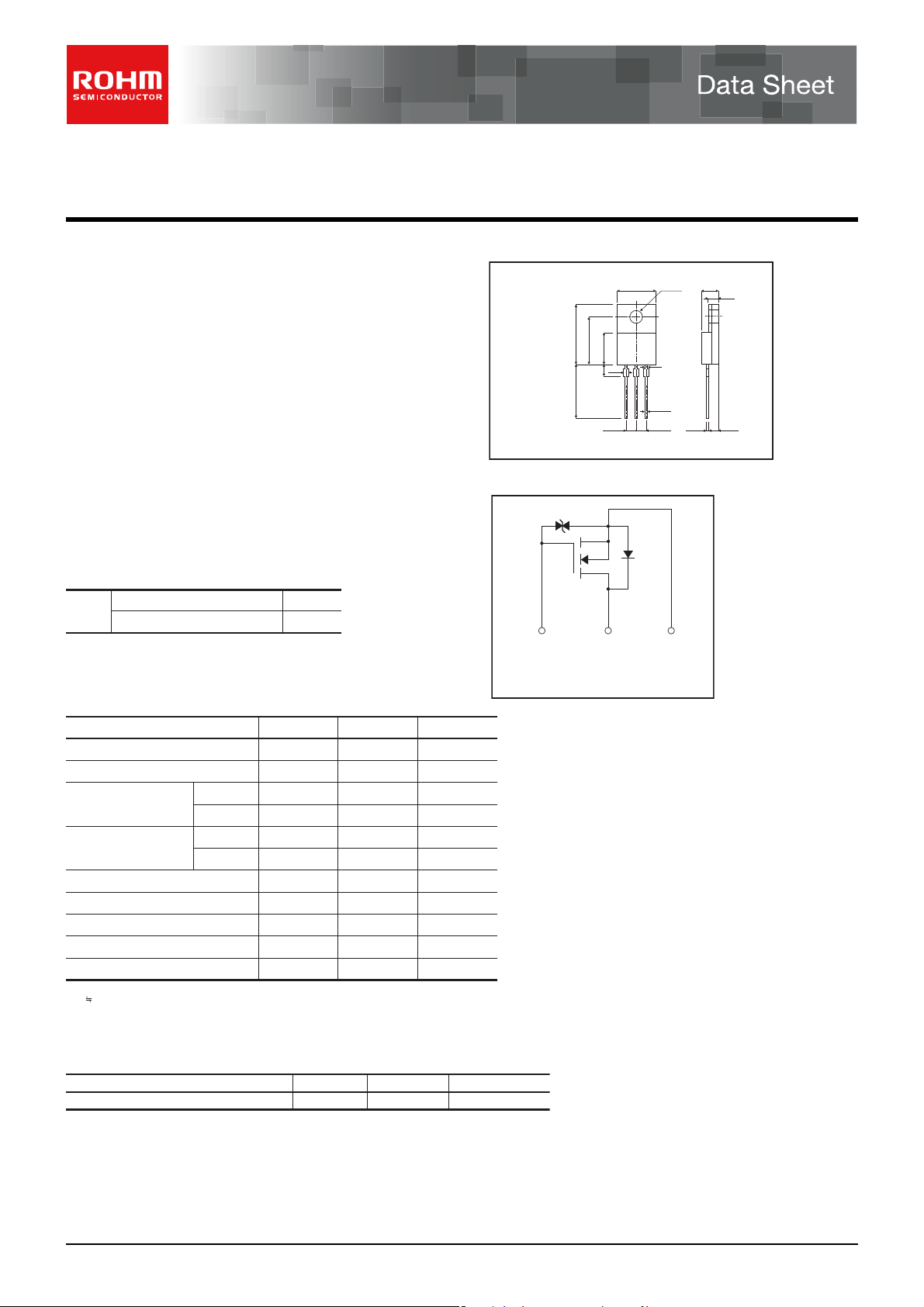
Structure Dimensions (Unit : mm)
Silicon N-channel MOSFET
Features
1) Low on-resistance.
2) Fast switching speed.
3) Gate-source voltage (V
GSS) guaranteed to be 30V.
4) Drive circuits can be simple.
5) Parallel use is easy.
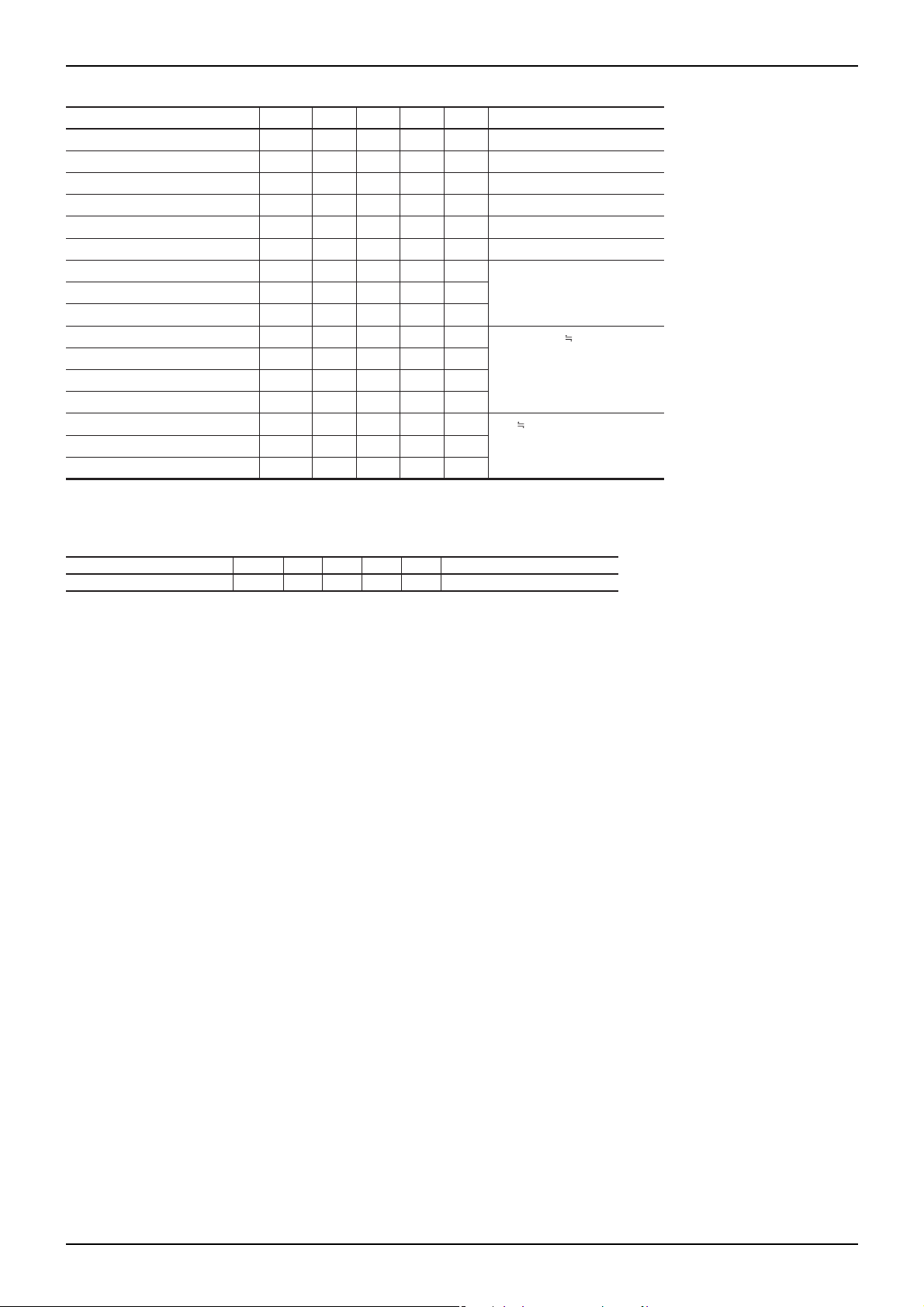
Applications Inner circuit
Switching
Packaging specifications
Package
Type
Basic ordering unit (pieces) 500pcs
Bulk
Absolute maximum ratings (Ta=25C)
∗3
∗1
∗3
∗1
∗2
∗2
−55 to +150
Limits
500
±30
±5
±20
5
20
2.5
1.6
40
150
Unit
V
V
A
A
A
A
A
mJ
W
°C
Parameter
Drain-source voltage
Gate-source voltage
Drain current
Source current
(Body Diode)
Continuous
Pulsed
Continuous
Pulsed
Avalanche current
Avalanche energy
Total power dissipation (Tc=25°C)
Channel temperature
Range of storage temperature
∗1 Pw≤10μs, Duty cycle≤1%
∗2 L 500μH, V
∗3 Limited only by maximum temperature allowed
DD
=50V, RG=25Ω, Starting, Tch=25°C
Symbol
V
DSS
V
GSS
I
D
I
DP
I
S
SP
I
AS
I
AS
E
P
D
Tch
Tstg °C
Thermal resistance
Parameter
hannel to case 3.13
Symbol Limits Unit
Rth(ch-c)
TO-220FM
(1)Base
(2)Collector
(3)Emitter
∗2
(1) (2) (3)
∗1 Body Diode
∗2 ESD Protection Diode
°C/W
10.0
15.0
12.0
8.02.5
1.3
14.0
(2)(3)(1)
∗1
φ
3.2
1.2
0.8
2.54 2.62.54
(1) Gate
(2) Drain
(3) Source
4.5
2.8
0.75
www.rohm.com
c
○
2012 ROHM Co., Ltd. All rights reserved.
1/3
2012.05 - Rev.B
R5005CNX
Electrical characteristics (Ta=25C)
Parameter
Symbol
Gate-source leakage
Drain-source breakdown voltage
V
Zero gate voltage drain current
Gate threshold voltage
Static drain-source on-state resistance
Forward transfer admittance
Input capacitance
Output capacitance
Reverse transfer capacitance
Turn-on delay time
Rise time
Turn-off delay time
Fall time
Total gate charge
Gate-source charge
Gate-drain charge
∗ Pulsed
I
(BR)DSS
I
V
R
| Y
C
C
t
t
Q
GSS
DSS
GS(th)
DS(on)
fs |
C
iss
oss
rss
d(on)
t
r
d(off)
t
f
Q
g
Q
gs
gd
Min.
−
500
−
2.5
∗
−
∗
1.5
−
−
−
∗
−
∗
−
∗
−
∗
−
∗
−
∗
−
∗
−
Body diode characteristics (Source-drain) (Ta=25C)
Parameter Symbol
∗ Pulsed
Min. Typ. Max.
∗
V
SD
−−1.5 V IS= 5A, VGS=0VForward voltage
Max. Unit Conditions
Typ.
GS
−
−
−
−
1.3
−
320
180
15
20
25
40
20
10.8
3.2
4.4
±10
100
−
4.5
1.6
−
−
−
−
μAV
V
μA
V
Ω
S
pF
pF
pF
− ns
− VGS=10Vns
− RL=100Ωns
− RG=10Ωns
nC
− V
− nC
− nC
Unit
=±30V, VDS=0V
D
=1mA, VGS=0V
I
DS
=500V, VGS=0V
V
DS
=10V, ID=1mA
V
I
D
=2.5A, VGS=10V
D
=2.5A, VDS=10V
I
V
DS
=25V
GS
=0V
V
f=1MHz
I
D
=2.5A, VDD 250V
DD
D
=5A
I
GS
=10V
V
L
=50Ω / RG=10Ω
R
Conditions
250V
Data Sheet
www.rohm.com
c
○
2012 ROHM Co., Ltd. All rights reserved.
2/3
2012.05 - Rev.B

R5005CNX
Measurement circuit
Fig.1 Switching time measurement circuit Fig.2 Switching waveforms
IG(Const.)
Fig.3 Gate charge measurement circuit Fig.4 Gate charge waveform
Fig.5 Avalanche measurement circuit Fig.6 Avalanche waveform
Data Sheet
www.rohm.com
c
○
2012 ROHM Co., Ltd. All rights reserved.
3/3
2012.05 - Rev.B

Notes
No copying or reproduction of this document, in part or in whole, is permitted without the
consent of ROHM Co.,Ltd.
The content specied herein is subject to change for improvement without notice.
The content specied herein is for the purpose of introducing ROHM's products (hereinafter
"Products"). If you wish to use any such Product, please be sure to refer to the specications,
which can be obtained from ROHM upon request.
Examples of application circuits, circuit constants and any other information contained herein
illustrate the standard usage and operations of the Products. The peripheral conditions must
be taken into account when designing circuits for mass production.
Great care was taken in ensuring the accuracy of the information specied in this document.
However, should you incur any damage arising from any inaccuracy or misprint of such
information, ROHM shall bear no responsibility for such damage.
The technical information specied herein is intended only to show the typical functions of and
examples of application circuits for the Products. ROHM does not grant you, explicitly or
implicitly, any license to use or exercise intellectual property or other rights held by ROHM and
other parties. ROHM shall bear no responsibility whatsoever for any dispute arising from the
use of such technical information.
The Products specied in this document are intended to be used with general-use electronic
equipment or devices (such as audio visual equipment, ofce-automation equipment, communication devices, electronic appliances and amusement devices).
The Products specied in this document are not designed to be radiation tolerant.
While ROHM always makes efforts to enhance the quality and reliability of its Products, a
Product may fail or malfunction for a variety of reasons.
Please be sure to implement in your equipment using the Products safety measures to guard
against the possibility of physical injury, re or any other damage caused in the event of the
failure of any Product, such as derating, redundancy, re control and fail-safe designs. ROHM
shall bear no responsibility whatsoever for your use of any Product outside of the prescribed
scope or not in accordance with the instruction manual.
The Products are not designed or manufactured to be used with any equipment, device or
system which requires an extremely high level of reliability the failure or malfunction of which
may result in a direct threat to human life or create a risk of human injury (such as a medical
instrument, transportation equipment, aerospace machinery, nuclear-reactor controller, fuelcontroller or other safety device). ROHM shall bear no responsibility in any way for use of any
of the Products for the above special purposes. If a Product is intended to be used for any
such special purpose, please contact a ROHM sales representative before purchasing.
If you intend to export or ship overseas any Product or technology specied herein that may
be controlled under the Foreign Exchange and the Foreign Trade Law, you will be required to
obtain a license or permit under the Law.
Notice
Thank you for your accessing to ROHM product informations.
More detail product informations and catalogs are available, please contact us.
ROHM Customer Support System
www.rohm.com
© 2012 ROHM Co., Ltd. All rights reserved.
http://www.rohm.com/contact/
R1120A
 Loading...